US6150702A - Lateral high-voltage semiconductor device having an outwardly extended electrode - Google Patents
Lateral high-voltage semiconductor device having an outwardly extended electrode Download PDFInfo
- Publication number
- US6150702A US6150702A US09/340,721 US34072199A US6150702A US 6150702 A US6150702 A US 6150702A US 34072199 A US34072199 A US 34072199A US 6150702 A US6150702 A US 6150702A
- Authority
- US
- United States
- Prior art keywords
- field plate
- field
- semiconductor device
- electrode
- plate
- Prior art date
- Legal status (The legal status is an assumption and is not a legal conclusion. Google has not performed a legal analysis and makes no representation as to the accuracy of the status listed.)
- Expired - Fee Related
Links
Images
Classifications
-
- H—ELECTRICITY
- H10—SEMICONDUCTOR DEVICES; ELECTRIC SOLID-STATE DEVICES NOT OTHERWISE PROVIDED FOR
- H10D—INORGANIC ELECTRIC SEMICONDUCTOR DEVICES
- H10D64/00—Electrodes of devices having potential barriers
- H10D64/111—Field plates
- H10D64/112—Field plates comprising multiple field plate segments
-
- H—ELECTRICITY
- H10—SEMICONDUCTOR DEVICES; ELECTRIC SOLID-STATE DEVICES NOT OTHERWISE PROVIDED FOR
- H10D—INORGANIC ELECTRIC SEMICONDUCTOR DEVICES
- H10D64/00—Electrodes of devices having potential barriers
- H10D64/20—Electrodes characterised by their shapes, relative sizes or dispositions
- H10D64/23—Electrodes carrying the current to be rectified, amplified, oscillated or switched, e.g. sources, drains, anodes or cathodes
-
- H—ELECTRICITY
- H10—SEMICONDUCTOR DEVICES; ELECTRIC SOLID-STATE DEVICES NOT OTHERWISE PROVIDED FOR
- H10D—INORGANIC ELECTRIC SEMICONDUCTOR DEVICES
- H10D8/00—Diodes
- H10D8/411—PN diodes having planar bodies
Definitions
- This invention relates to a high-voltage semiconductor device, and more particularly to a lateral high-voltage semiconductor device with high breakdown strength at the corners of the field plates.
- electrodes are provided in the same plane. To form an IC by connecting each element, the electrodes have to be connected to one another.
- a field plate is provided in an area between the high-voltage section and the low-voltage section via a field oxide film to alleviate the electric field at the surface of the semiconductor device.
- a thick field oxide film is required to achieve high breakdown strength.
- the thick field oxide film makes the processing very difficult and the breakdown strength may be deteriorated due to a reliability test.
- a method has been tried.
- a high-resistance film such as an SIPOS film
- Leakage current is allowed to flow over the film.
- Use of such a high-resistance film causes a rise in the cost and a reliability problem.
- FIG. 6 is a plan view of a conventional high-voltage semiconductor device using this type of field plate.
- FIG. 7 is a sectional view taken along line VII--VII of FIG. 6.
- FIGS. 6 and 7 show a lateral diode as an example of high-voltage semiconductor device.
- numeral "1" indicates a substrate
- "2" indicates an SiO 2 film
- "3" indicates a high-resistance n-type cathode layer formed in a silicon substrate (SOI).
- SOI silicon substrate
- a p-type anode layer 4 and an n-type cathode layer 5 are selectively formed.
- a high-impurity-concentration p-type contact layer 6 and a high-impurity-concentration n-type contact layer 7 are selectively formed, respectively.
- a LOCOS oxide film 8 is formed on the surface of the n-type cathode layer 3 in the area between the p-type anode layer 4 and the n-type cathode layer 5.
- a spiral field plate 9 composed of a polysilicon film is formed on the LOCOS oxide film 8.
- the field plate 9 is composed of a track-like first field plate 9 1 connected to an anode electrode 10, a track-like second field plate 9 2 which is surrounded by the first field plate 9 1 and is connected to a cathode electrode 11, and a spiral field plate 9a one end of which is connected to the first field plate 9 1 and the other end of which is connected to the second field plate 9 2 .
- Numeral "12" indicates an interlayer insulating film.
- the spiral pitch of the field plate 9a is set narrow.
- the element width W becomes greater and the total length of the field plate 9 becomes larger, leakage current decreases in the field plate 9. If spiral field plate 9a is particularly narrow, almost no leakage current flows. As a result, it is difficult to maintain the uniform electric field, degrading the breakdown strength.
- the electrodes connected to the semiconductor region in the central portion of the device are provided in such a manner that they cross the other regions. Because of the effect of an electric field caused by the currents flowing through the electrodes, a breakdown is liable to take place at and near the electrodes, which is a problem peculiar to the lateral semiconductor element.
- the object of the present invention is to provide a lateral high-voltage semiconductor device with a field plate capable of suppressing the degradation of breakdown strength even when the width of high-voltage semiconductor elements becomes greater and capable of alleviating the effect of an electric field caused by the electrodes.
- a lateral high-voltage semiconductor device comprising a first semiconductor region; a second semiconductor region; a field plate arranged between the first semiconductor region and the second semiconductor regions; a first electrode being connected to the first semiconductor region, and being arranged in a manner such that the first electrode crosses over the field plate and extends outwardly; a second electrode connected to the second semiconductor region; and a first current path located below the first electrode and connected to the field plate in a manner such that the first current path crosses the field plate.
- a lateral high-voltage semiconductor device comprising: a semiconductor substrate; a first conductivity-type semiconductor region selectively formed at the surface of the semiconductor substrate; a second conductivity-type semiconductor region being selectively formed at the surface of the semiconductor substrate; a field insulating film being provided on the semiconductor substrate to be located between the first conductivity-type semiconductor region and the second conductivity-type semiconductor region; a first field plate being provided on the field insulating film so as to surround the first conductivity-type semiconductor region, the first field plate being electrically connected to the first conductivity-type semiconductor region; a second field plate being provided on the field insulating film, and being electrically connected to the second conductivity-type semiconductor region; at least one third field plate being provided concentrically on the field insulating film, the at least one third field plate being arranged between the first field plate and the second field plate; at least one fourth field plate for connecting the first field plate, the third field plates, and the second field plate; and an electrode being connected to the first
- a lateral high-voltage semiconductor device having a first conductive region, a second conductive region surrounding the first conductive region, a field plate interposed between the first and second conductive regions, and an electrode extended outwardly from the first conductive region over the field plate, the field plate comprising: at least one first electric field generating element located at the corner section of the field plate; at least one second electric field generating element which is connected to the first electric field generating element and has a resistance higher than the first electric field generating element; and at least one current supply path for supplying current to the first electric field generating element and the second electric field generating element.
- the use of band-like field plates enables the degradation of breakdown strength to be suppressed without decreasing the current flowing in the field plate, even when the high-voltage semiconductor element has a wide width.
- the degradation of breakdown strength is further suppressed by connecting the field plates so as to allow more current to flow below the electrodes and around the corner sections where a breakdown is likely to take place.
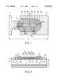
- FIG. 1 is a plan view of a high-voltage semiconductor device according to a first embodiment of the present invention
- FIG. 2 is a sectional view taken along line II--II of FIG. 1;
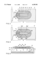
- FIG. 3 is a plan view of a high-voltage semiconductor device according to a second embodiment of the present invention.
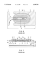
- FIG. 4 is a plan view of a high-voltage semiconductor device according to a third embodiment of the present invention.
- FIG. 5 is a plan view of a high-voltage semiconductor device according to a modification of the present invention.
- FIG. 6 is a plan view of a conventional high-voltage semiconductor device.
- FIG. 7 is a sectional view taken along line VII--VII of FIG. 6.
- FIG. 1 is a plan view of a high-voltage semiconductor device according to a first embodiment of the present invention.
- FIG. 1 shows an example of using a lateral diode as a high-voltage semiconductor element.
- FIG. 2 is a sectional view taken along line II--II of FIG. 1.
- a field plate 9 is composed of a track-like first field plate 9 1 connected to an anode electrode 10, a track-like second field plate 9 2 which is surrounded by the first field plate 9 1 and is connected to a cathode electrode 11, track-like field plates 9 1 to 9 9 arranged concentrically at regular intervals between the first and second field plates 9 1 and 9 2 , and linear field plates 9 10 connecting adjacent plates 9 1 to 9 9 .
- the field plates 9 10 connect the adjacent ones of field plates 9 1 to 9 9 in one place at their corner sections and in two places at their straight-line sections.
- the linear field plates 9 10 connect the adjacent ones of field plates 9 1 to 9 9 to allow a large current to flow in the corner sections of the plates 9 1 to 9 9 located below the extended portion 11 ext (lead-out electrode) of the cathode electrode 11, in other words, to allow a large current to flow the portion of the field plates 9 1 to 9 9 located above the region where an electric field is liable to concentrate.
- the field plates 9 1 to 9 9 may be connected in the same manner at the other corner sections, for example, by using field plates 9 10' and/or field plates 9 10" .
- the total length of the current path consisting of field plates 9 1 to 9 9 and linear field plates 9 10 at the corner section is shorter than that at the straight section.
- the current path at the corner section has a resistance smaller than the current path at the straight section. Because of the resistance difference, the current flowing in the corner sections of the plates 9 1 to 9 9 above the region where an electric field is liable to concentrate increases, a leakage current having a sufficient amount to produce the field plate effect is allowed to flow in the corner sections, even when the greater element width W makes the total length of the field plate 9 larger. This makes it possible to produce a uniform electric field in the corner sections even when the width W of the elements becomes greater, suppressing the degradation of the breakdown strength. Furthermore, when the element width W remains unchanged, the breakdown strength can be increased.
- FIG. 3 is a plan view of a high-voltage semiconductor device according to a second embodiment of the present invention.
- the same parts as those in the first embodiment are indicated by the same reference symbols and detailed explanation of them is omitted.
- the second embodiment differs from the first embodiment in that the adjacent field plates 9 1 to 9 9 are connected by linear field plates 9 10 in a zigzag manner only under the extended portion 11 ext (lead-out electrode) of the cathode electrode 11.
- the current flowing in the corner sections of the field plates 9 1 to 9 9 near the cathode electrode 11 further increases, whereas the current flowing in the straight line sections further decreases. Consequently, if the leakage current flowing in the field plate 9 remains unchanged, the breakdown strength in the corner sections of the cathode electrode 11 will increase more than in the first embodiment.
- FIG. 4 is a plan view of a high-voltage semiconductor device according to a third embodiment of the present invention.
- the same parts as those in the first embodiment are indicated by the same reference symbols and detailed explanation of them will not be given.
- the third embodiment has a feature that the portions of field plates 9 1 to 9 9 located below the extended portion llext (lead-out electrode) of the cathode electrode 11 are connected by linear field plates 9 10 arranged linearly.
- the field plates 9 1 to 9 9 may be connected at the opposite side by another linear field plate 9 10' . Further, the field plates 9 1 to 9 9 may be connected at the straight section, for example in a manner as shown in FIG. 4, where field plates 9 1 to 9 9 are connected by four linear field plates 9 10" in a zigzag manner.
- the breakdown strength at the corner section can be improved reliably without increasing the leakage current.
- the value of the leakage current (the one drawn by the field plate 9 from the current originally to flow in the elements) in the first to third embodiments is of the order of microamperes, there is no problem.
- the present invention is not limited to the above embodiments.
- the lateral diode has been used, the invention may be applied to other lateral power semiconductor elements, including lateral power MOS transistors and lateral IGBTs.
- FIG. 5 is a sectional view of a lateral power MOS transistor to which the present invention has been applied.
- numeral "21" indicates a high-impurity-concentration n-type source layer
- "22” indicates a p-type well layer
- "23” indicates a high-impurity-concentration n-type drain layer
- "24” indicates a source electrode
- "25” indicates a drain electrode
- "26” indicates a gate oxide film
- “27” indicates a gate electrode.
- the invention is applied to an IGBT, the n-type drain layer 23 has to be replaced with a p-type drain layer. While in FIG. 5, the field plate structure of the first embodiment has been used, the field plate structure of the other embodiments may be applied.
- the SOI substrate has been used, other semiconductor substrate may be used.
- the SOI substrate the one formed by a direct adhesion method should be used.
- field plates 9 10 , 9 10' , and 9 10" connect the individual track-like field plates one another to reduce the resistance of the current path above the region where an electric field is liable to concentrate. This enables a uniform electric field to be generated in the region where an electric field is liable to concentrate even when the element has a large width, which prevents the breakdown strength from deteriorating.
- field plates 9 10 are provided to allow more current to flow below the electrode and in the corner section where a breakdown is liable to take place. This further suppresses the degradation of the breakdown strength above the region where an electric field is liable to take place.
- the present invention is particularly useful for a lateral semiconductor device with electrodes crossing the field plates.
Landscapes
- Insulated Gate Type Field-Effect Transistor (AREA)
- Electrodes Of Semiconductors (AREA)
Abstract
The breakdown strength of a lateral diode using a field plate is improved. There are provided a track-like first field plate connected to an anode electrode, a track-like second field plate formed outside the first field plate and connected to a cathode electrode, track-like third field plates provided concentrically between the first and second field plates, and fourth field plates provided so as to cross the first to third field plates and connected to each of them. The fourth field plates are so positioned that they allow more current to flow in the corner sections and under the electrodes where an electric field is liable to concentrate.
Description
This invention relates to a high-voltage semiconductor device, and more particularly to a lateral high-voltage semiconductor device with high breakdown strength at the corners of the field plates.
In conventional high-voltage semiconductor elements used for power ICs, electrodes are provided in the same plane. To form an IC by connecting each element, the electrodes have to be connected to one another.
In general, a field plate is provided in an area between the high-voltage section and the low-voltage section via a field oxide film to alleviate the electric field at the surface of the semiconductor device.
A thick field oxide film is required to achieve high breakdown strength. The thick field oxide film makes the processing very difficult and the breakdown strength may be deteriorated due to a reliability test.
To overcome the problems, a method has been tried. In the method, a high-resistance film, such as an SIPOS film, is used to produce a uniform electric field in the lateral direction of the field oxide film. Leakage current is allowed to flow over the film. Use of such a high-resistance film, however, causes a rise in the cost and a reliability problem.
To avoid the problems, another method has been considered. In the method, a high-resistance silicon film is used as a field plate and made as narrow as possible. The narrow film connects the anode and cathode of each element. FIG. 6 is a plan view of a conventional high-voltage semiconductor device using this type of field plate. FIG. 7 is a sectional view taken along line VII--VII of FIG. 6. FIGS. 6 and 7 show a lateral diode as an example of high-voltage semiconductor device.
In the figures, numeral "1" indicates a substrate, "2" indicates an SiO2 film, "3" indicates a high-resistance n-type cathode layer formed in a silicon substrate (SOI). At the surface of the n-type cathode layer 3, a p-type anode layer 4 and an n-type cathode layer 5 are selectively formed. At the surfaces of the p-type anode layer 4 and n-type cathode layer 5, a high-impurity-concentration p-type contact layer 6 and a high-impurity-concentration n-type contact layer 7 are selectively formed, respectively.
On the surface of the n-type cathode layer 3 in the area between the p-type anode layer 4 and the n-type cathode layer 5, a LOCOS oxide film 8 is formed. On the LOCOS oxide film 8, a spiral field plate 9 composed of a polysilicon film is formed.
The field plate 9 is composed of a track-like first field plate 91 connected to an anode electrode 10, a track-like second field plate 92 which is surrounded by the first field plate 91 and is connected to a cathode electrode 11, and a spiral field plate 9a one end of which is connected to the first field plate 91 and the other end of which is connected to the second field plate 92. Numeral "12" indicates an interlayer insulating film.
To produce a uniform electric field needed to alleviate the electric field, the spiral pitch of the field plate 9a is set narrow. When the element width W becomes greater and the total length of the field plate 9 becomes larger, leakage current decreases in the field plate 9. If spiral field plate 9a is particularly narrow, almost no leakage current flows. As a result, it is difficult to maintain the uniform electric field, degrading the breakdown strength.
In a lateral semiconductor device having the above-mentioned structure, the electrodes connected to the semiconductor region in the central portion of the device are provided in such a manner that they cross the other regions. Because of the effect of an electric field caused by the currents flowing through the electrodes, a breakdown is liable to take place at and near the electrodes, which is a problem peculiar to the lateral semiconductor element.
The object of the present invention is to provide a lateral high-voltage semiconductor device with a field plate capable of suppressing the degradation of breakdown strength even when the width of high-voltage semiconductor elements becomes greater and capable of alleviating the effect of an electric field caused by the electrodes.
According to a first aspect of the present invention, there is provided a lateral high-voltage semiconductor device comprising a first semiconductor region; a second semiconductor region; a field plate arranged between the first semiconductor region and the second semiconductor regions; a first electrode being connected to the first semiconductor region, and being arranged in a manner such that the first electrode crosses over the field plate and extends outwardly; a second electrode connected to the second semiconductor region; and a first current path located below the first electrode and connected to the field plate in a manner such that the first current path crosses the field plate.
According to a second aspect of the present invention, there is provided a lateral high-voltage semiconductor device comprising: a semiconductor substrate; a first conductivity-type semiconductor region selectively formed at the surface of the semiconductor substrate; a second conductivity-type semiconductor region being selectively formed at the surface of the semiconductor substrate; a field insulating film being provided on the semiconductor substrate to be located between the first conductivity-type semiconductor region and the second conductivity-type semiconductor region; a first field plate being provided on the field insulating film so as to surround the first conductivity-type semiconductor region, the first field plate being electrically connected to the first conductivity-type semiconductor region; a second field plate being provided on the field insulating film, and being electrically connected to the second conductivity-type semiconductor region; at least one third field plate being provided concentrically on the field insulating film, the at least one third field plate being arranged between the first field plate and the second field plate; at least one fourth field plate for connecting the first field plate, the third field plates, and the second field plate; and an electrode being connected to the first conductivity-type semiconductor region, the electrode extending outwardly in such a manner that the electrode crosses over the first, second, third, and fourth field plates, wherein the fourth field plate is located below the electrode.
According to a third aspect of the present invention, there is provided a lateral high-voltage semiconductor device having a first conductive region, a second conductive region surrounding the first conductive region, a field plate interposed between the first and second conductive regions, and an electrode extended outwardly from the first conductive region over the field plate, the field plate comprising: at least one first electric field generating element located at the corner section of the field plate; at least one second electric field generating element which is connected to the first electric field generating element and has a resistance higher than the first electric field generating element; and at least one current supply path for supplying current to the first electric field generating element and the second electric field generating element.
According to the present invention, the use of band-like field plates enables the degradation of breakdown strength to be suppressed without decreasing the current flowing in the field plate, even when the high-voltage semiconductor element has a wide width.
Furthermore, according to the present invention, the degradation of breakdown strength is further suppressed by connecting the field plates so as to allow more current to flow below the electrodes and around the corner sections where a breakdown is likely to take place.
Additional objects and advantages of the invention will be set forth in the description which follows, and in part will be obvious from the description, or may be learned by practice of the invention. The objects and advantages of the invention may be realized and obtained by means of the instrumentalities and combinations particularly pointed out hereinafter.
The accompanying drawings, which are incorporated in and constitute a part of the specification, illustrate presently preferred embodiments of the invention, and together with the general description given above and the detailed description of the preferred embodiments given below, serve to explain the principles of the invention.
FIG. 1 is a plan view of a high-voltage semiconductor device according to a first embodiment of the present invention;
FIG. 2 is a sectional view taken along line II--II of FIG. 1;
FIG. 3 is a plan view of a high-voltage semiconductor device according to a second embodiment of the present invention;
FIG. 4 is a plan view of a high-voltage semiconductor device according to a third embodiment of the present invention;
FIG. 5 is a plan view of a high-voltage semiconductor device according to a modification of the present invention;
FIG. 6 is a plan view of a conventional high-voltage semiconductor device; and
FIG. 7 is a sectional view taken along line VII--VII of FIG. 6.
Hereinafter, referring to the accompanying drawings, embodiments of the present invention will be explained.
(First Embodiment)
FIG. 1 is a plan view of a high-voltage semiconductor device according to a first embodiment of the present invention.
FIG. 1 shows an example of using a lateral diode as a high-voltage semiconductor element. FIG. 2 is a sectional view taken along line II--II of FIG. 1.
In the first embodiment, a field plate 9 is composed of a track-like first field plate 91 connected to an anode electrode 10, a track-like second field plate 92 which is surrounded by the first field plate 91 and is connected to a cathode electrode 11, track-like field plates 91 to 99 arranged concentrically at regular intervals between the first and second field plates 91 and 92, and linear field plates 910 connecting adjacent plates 91 to 99. The field plates 910 connect the adjacent ones of field plates 91 to 99 in one place at their corner sections and in two places at their straight-line sections.
The linear field plates 910 connect the adjacent ones of field plates 91 to 99 to allow a large current to flow in the corner sections of the plates 91 to 99 located below the extended portion 11ext (lead-out electrode) of the cathode electrode 11, in other words, to allow a large current to flow the portion of the field plates 91 to 99 located above the region where an electric field is liable to concentrate. The field plates 91 to 99 may be connected in the same manner at the other corner sections, for example, by using field plates 910' and/or field plates 910".
Regarding the first embodiment, the total length of the current path consisting of field plates 91 to 99 and linear field plates 910 at the corner section is shorter than that at the straight section. Under the condition that those field plates are designed to have the same electric resistivity, e.g., the same width and thickness, the current path at the corner section has a resistance smaller than the current path at the straight section. Because of the resistance difference, the current flowing in the corner sections of the plates 91 to 99 above the region where an electric field is liable to concentrate increases, a leakage current having a sufficient amount to produce the field plate effect is allowed to flow in the corner sections, even when the greater element width W makes the total length of the field plate 9 larger. This makes it possible to produce a uniform electric field in the corner sections even when the width W of the elements becomes greater, suppressing the degradation of the breakdown strength. Furthermore, when the element width W remains unchanged, the breakdown strength can be increased.
(Second Embodiment)
FIG. 3 is a plan view of a high-voltage semiconductor device according to a second embodiment of the present invention. The same parts as those in the first embodiment are indicated by the same reference symbols and detailed explanation of them is omitted.
The second embodiment differs from the first embodiment in that the adjacent field plates 91 to 99 are connected by linear field plates 910 in a zigzag manner only under the extended portion 11ext (lead-out electrode) of the cathode electrode 11.
With the second embodiment, the current flowing in the corner sections of the field plates 91 to 99 near the cathode electrode 11 further increases, whereas the current flowing in the straight line sections further decreases. Consequently, if the leakage current flowing in the field plate 9 remains unchanged, the breakdown strength in the corner sections of the cathode electrode 11 will increase more than in the first embodiment.
(Third Embodiment)
FIG. 4 is a plan view of a high-voltage semiconductor device according to a third embodiment of the present invention. The same parts as those in the first embodiment are indicated by the same reference symbols and detailed explanation of them will not be given.
The third embodiment has a feature that the portions of field plates 91 to 99 located below the extended portion llext (lead-out electrode) of the cathode electrode 11 are connected by linear field plates 910 arranged linearly. The field plates 91 to 99 may be connected at the opposite side by another linear field plate 910'. Further, the field plates 91 to 99 may be connected at the straight section, for example in a manner as shown in FIG. 4, where field plates 91 to 99 are connected by four linear field plates 910" in a zigzag manner.
If high-resistance polysilicon films, for example, narrow polysilicon films, are used as the field plate 910', the breakdown strength at the corner section can be improved reliably without increasing the leakage current.
As long as the value of the leakage current (the one drawn by the field plate 9 from the current originally to flow in the elements) in the first to third embodiments is of the order of microamperes, there is no problem.
The present invention is not limited to the above embodiments. For instance, in the above embodiments, the lateral diode has been used, the invention may be applied to other lateral power semiconductor elements, including lateral power MOS transistors and lateral IGBTs.
FIG. 5 is a sectional view of a lateral power MOS transistor to which the present invention has been applied. In FIG. 5, numeral "21" indicates a high-impurity-concentration n-type source layer, "22" indicates a p-type well layer, "23" indicates a high-impurity-concentration n-type drain layer, "24" indicates a source electrode, "25" indicates a drain electrode, "26" indicates a gate oxide film, and "27" indicates a gate electrode. When the invention is applied to an IGBT, the n-type drain layer 23 has to be replaced with a p-type drain layer. While in FIG. 5, the field plate structure of the first embodiment has been used, the field plate structure of the other embodiments may be applied.
While in the above embodiments, the SOI substrate has been used, other semiconductor substrate may be used. For the SOI substrate, the one formed by a direct adhesion method should be used.
The present invention may be practiced or embodied in still other ways without departing from the spirit or essential character thereof.
Regarding the present invention, field plates 910, 910', and 910", connect the individual track-like field plates one another to reduce the resistance of the current path above the region where an electric field is liable to concentrate. This enables a uniform electric field to be generated in the region where an electric field is liable to concentrate even when the element has a large width, which prevents the breakdown strength from deteriorating.
Furthermore, in the invention, field plates 910 are provided to allow more current to flow below the electrode and in the corner section where a breakdown is liable to take place. This further suppresses the degradation of the breakdown strength above the region where an electric field is liable to take place.
The present invention is particularly useful for a lateral semiconductor device with electrodes crossing the field plates.
Additional advantages and modifications will readily occur to those skilled in the art. Therefore, the invention in its broader aspects is not limited to the specific details and representative embodiments shown and described herein. Accordingly, various modifications may be made without departing from the spirit or scope of the general inventive concept as defined by the appended claims and their equivalents.
Claims (20)
1. A lateral high-voltage semiconductor device comprising:
a first semiconductor region;
a second semiconductor region;
a field plate arranged between said first semiconductor region and said second semiconductor regions;
a first electrode being connected to said first semiconductor region, and being arranged in a manner such that said first electrode crosses over said field plate and extends outwardly;
a second electrode connected to said second semiconductor region; and
a first current path located below said first electrode and connected to said field plate in a manner such that said first current path crosses said field plate.
2. The lateral high-voltage semiconductor device according to claim 1, wherein said field plate has at least one band-like conductor being arranged to surround said first semiconductor region, said at least one band-like conductor being connected to said first electrode and said second electrode through said first current path.
3. The lateral high-voltage semiconductor device according to claim 2, wherein said at least one band-like conductor includes at least one ringed conductor arranged concentrically with said first semiconductor region in the center.
4. The lateral high-voltage semiconductor device according to claim 3, wherein said first current path comprises at least one conductive line for connecting said at least one ringed conductor to said first electrode, and said second electrode.
5. The lateral high-voltage semiconductor device according to claim 4, wherein said at least one conductive line is provided in the form of a straight line.
6. A lateral high-voltage semiconductor device according to claim 4, wherein said at least one conductive line is provided zigzag.
7. The lateral high-voltage semiconductor device according to claim 4, wherein said ringed conductor and said conductive line are made of a polysilicon film.
8. The lateral high-voltage semiconductor device according to claim 1, further comprising at least one second current path for connecting said field plate to said first electrode and said second electrode, said at least one second current path being arranged to cross said field plate.
9. The lateral high-voltage semiconductor device according to claim 8, wherein said field plate is divided by said first current path and said second current path into a first subfield plate including the corner section and a second subfield plate adjoining said first subfield plate and having a higher resistance than said first subfield plate.
10. The lateral high-voltage semiconductor device according to claim 9, wherein said first subfield plate is shorter in length than said second subfield plate.
11. A lateral high-voltage semiconductor device comprising:
a semiconductor substrate;
a first conductivity-type semiconductor region selectively formed at the surface of said semiconductor substrate;
a second conductivity-type semiconductor region being selectively formed at the surface of said semiconductor substrate;
a field insulating film being provided on said semiconductor substrate to be located between said first conductivity-type semiconductor region and said second conductivity-type semiconductor region;
a first field plate being provided on said field insulating film so as to surround said first conductivity-type semiconductor region, said first field plate being electrically connected to said first conductivity-type semiconductor region;
a second field plate being provided on said field insulating film, and being electrically connected to said second conductivity-type semiconductor region;
at least one third field plate being provided concentrically on said field insulating film, said at least one third field plate being arranged between said first field plate and said second field plate;
at least one fourth field plate for connecting said first field plate, said third field plates, and said second field plate to one another; and
an electrode being connected to said first conductivity-type semiconductor region, said electrode extending outwardly in such a manner that said electrode crosses over said first, second, third, and fourth field plates,
wherein said fourth field plate is located below said electrode.
12. The lateral high-voltage semiconductor device according to claim 11, wherein said fourth field plate comprises at least one conductive film for connecting said first field plate, third field plates, and second field plate to one another.
13. The lateral high-voltage semiconductor device according to claim 12, wherein said conductive film is arranged linearly along said electrode.
14. The lateral high-voltage semiconductor device according to claim 12, wherein said conductive film is provided zigzag in the longitudinal direction of said electrode.
15. The lateral high-voltage semiconductor device according to claim 12, further comprising at least one fifth field plate being arranged to cross said third field plate, said fifth field plate connecting a part of said third field plate to said first field plate and connecting another part of said third field plate to said second field plate.
16. The lateral high-voltage semiconductor device according to claim 15, wherein said third field plate are divided by said fourth and fifth field plates into a first subfield plate of an arc shape including corner sections and a second subfield plate of a straight line adjoining said first subfield plates and having a higher resistance than said first subfield plates.
17. The lateral high-voltage semiconductor device according to claim 16, wherein said first subfield plates are shorter in length than said second subfield plates.
18. A lateral high-voltage semiconductor device having a first conductive region, a second conductive region surrounding the first conductive region, a field plate interposed between the first and second conductive regions, and an electrode extended outwardly from the first conductive region over the field plate, said field plate comprising:
at least one first electric field generating element located at the corner section of said field plate;
at least one second electric field generating element which is connected to said first electric field generating element and has a resistance higher than said first electric field generating element; and
at least one current supply path for supplying current to said first electric field generating element and said second electric field generating element.
19. The lateral high-voltage semiconductor device according to claim 18, wherein at least one of said first electric field generating element is provided below said electrode.
20. The lateral high-voltage semiconductor device according to claim 19, wherein said current supply path is provided in such a manner that the current flowing through said first electric field generating element is greater than the current flowing through said second electric field generating element.
Applications Claiming Priority (2)
| Application Number | Priority Date | Filing Date | Title |
|---|---|---|---|
| JP10-199521 | 1998-06-30 | ||
| JP19952198A JP3905981B2 (en) | 1998-06-30 | 1998-06-30 | High voltage semiconductor device |
Publications (1)
| Publication Number | Publication Date |
|---|---|
| US6150702A true US6150702A (en) | 2000-11-21 |
Family
ID=16409220
Family Applications (1)
| Application Number | Title | Priority Date | Filing Date |
|---|---|---|---|
| US09/340,721 Expired - Fee Related US6150702A (en) | 1998-06-30 | 1999-06-29 | Lateral high-voltage semiconductor device having an outwardly extended electrode |
Country Status (2)
| Country | Link |
|---|---|
| US (1) | US6150702A (en) |
| JP (1) | JP3905981B2 (en) |
Cited By (20)
| Publication number | Priority date | Publication date | Assignee | Title |
|---|---|---|---|---|
| WO2001088992A3 (en) * | 2000-05-16 | 2002-05-30 | Bosch Gmbh Robert | Semiconductor power component |
| US6424014B2 (en) * | 2000-02-25 | 2002-07-23 | Oki Electric Industry Co,Ltd. | Semiconductor element with electric field reducing device mounted therein for increasing dielectric strength |
| US6650001B2 (en) * | 2001-01-25 | 2003-11-18 | Kabushiki Kaisha Toshiba | Lateral semiconductor device and vertical semiconductor device |
| US20040251499A1 (en) * | 2003-06-11 | 2004-12-16 | Kabushiki Kaisha Toshiba | High withstand voltage semiconductor device |
| US20060270171A1 (en) * | 2005-05-25 | 2006-11-30 | Li-Che Chen | MOS transistor device structure combining Si-trench and field plate structures for high voltage device |
| CN1324717C (en) * | 2004-06-24 | 2007-07-04 | 东南大学 | Multi electric potential field plate lateral high voltage N type MOS transistor |
| US20080203496A1 (en) * | 2007-02-28 | 2008-08-28 | Mitsubishi Electric Corporation | Semiconductor device |
| US20080315343A1 (en) * | 2007-02-13 | 2008-12-25 | Kabushiki Kaisha Toshiba | Semiconductor device |
| US20100163987A1 (en) * | 2008-12-26 | 2010-07-01 | Rohm Co., Ltd. | Semiconductor device |
| CN101364612B (en) * | 2007-08-10 | 2011-06-01 | 联华电子股份有限公司 | High voltage MOS transistor |
| US20120032313A1 (en) * | 2010-08-04 | 2012-02-09 | Denso Corporation | Semiconductor device having lateral diode |
| US20120292740A1 (en) * | 2011-05-19 | 2012-11-22 | Macronix International Co., Ltd. | High voltage resistance semiconductor device and method of manufacturing a high voltage resistance semiconductor device |
| US20120299096A1 (en) * | 2011-05-29 | 2012-11-29 | Taiwan Semiconductor Manufacturing Co., Ltd. | High voltage and ultra-high voltage semiconductor devices with increased breakdown voltages |
| US20140077284A1 (en) * | 2012-09-19 | 2014-03-20 | Mitsubishi Electric Corporation | Semiconductor device |
| US9240445B2 (en) | 2011-05-13 | 2016-01-19 | Denso Corporation | Lateral semiconductor device |
| US9762048B2 (en) | 2015-12-15 | 2017-09-12 | Fuji Electric Co., Ltd. | Semiconductor device |
| US10217861B2 (en) | 2016-03-18 | 2019-02-26 | Fuji Electric Co., Ltd. | High voltage integrated circuit with high voltage junction termination region |
| US10396167B2 (en) | 2015-12-15 | 2019-08-27 | Fuji Electric Co., Ltd. | Semiconductor device |
| US10680072B2 (en) | 2017-09-25 | 2020-06-09 | Renesas Electronics Coporation | Semiconductor device and manufacturing method thereof |
| US12062687B2 (en) * | 2018-09-28 | 2024-08-13 | Taiwan Semiconductor Manufacturing Company, Ltd. | Semiconductor device including a capacitor |
Families Citing this family (9)
| Publication number | Priority date | Publication date | Assignee | Title |
|---|---|---|---|---|
| JP4894097B2 (en) * | 2001-06-27 | 2012-03-07 | 富士電機株式会社 | Semiconductor device |
| WO2003054972A1 (en) | 2001-12-12 | 2003-07-03 | Matsushita Electric Industrial Co., Ltd. | Variable capacitor and its manufacturing method |
| JP4469584B2 (en) | 2003-09-12 | 2010-05-26 | 株式会社東芝 | Semiconductor device |
| JP4731816B2 (en) * | 2004-01-26 | 2011-07-27 | 三菱電機株式会社 | Semiconductor device |
| JP4935880B2 (en) * | 2009-10-06 | 2012-05-23 | 株式会社デンソー | Semiconductor device |
| JP5460279B2 (en) * | 2009-12-11 | 2014-04-02 | 株式会社日立製作所 | Semiconductor device and manufacturing method thereof |
| JP6001309B2 (en) * | 2012-04-17 | 2016-10-05 | エスアイアイ・セミコンダクタ株式会社 | Semiconductor device |
| JP2015090952A (en) * | 2013-11-07 | 2015-05-11 | 株式会社豊田中央研究所 | Horizontal semiconductor device and manufacturing method thereof |
| JP6649102B2 (en) * | 2016-02-05 | 2020-02-19 | ルネサスエレクトロニクス株式会社 | Semiconductor device |
Citations (2)
| Publication number | Priority date | Publication date | Assignee | Title |
|---|---|---|---|---|
| JPH0677470A (en) * | 1992-06-24 | 1994-03-18 | Toshiba Corp | Semiconductor device |
| JPH07326775A (en) * | 1994-05-31 | 1995-12-12 | Sanken Electric Co Ltd | Semiconductor device |
-
1998
- 1998-06-30 JP JP19952198A patent/JP3905981B2/en not_active Expired - Fee Related
-
1999
- 1999-06-29 US US09/340,721 patent/US6150702A/en not_active Expired - Fee Related
Patent Citations (2)
| Publication number | Priority date | Publication date | Assignee | Title |
|---|---|---|---|---|
| JPH0677470A (en) * | 1992-06-24 | 1994-03-18 | Toshiba Corp | Semiconductor device |
| JPH07326775A (en) * | 1994-05-31 | 1995-12-12 | Sanken Electric Co Ltd | Semiconductor device |
Cited By (39)
| Publication number | Priority date | Publication date | Assignee | Title |
|---|---|---|---|---|
| US6424014B2 (en) * | 2000-02-25 | 2002-07-23 | Oki Electric Industry Co,Ltd. | Semiconductor element with electric field reducing device mounted therein for increasing dielectric strength |
| WO2001088992A3 (en) * | 2000-05-16 | 2002-05-30 | Bosch Gmbh Robert | Semiconductor power component |
| US6650001B2 (en) * | 2001-01-25 | 2003-11-18 | Kabushiki Kaisha Toshiba | Lateral semiconductor device and vertical semiconductor device |
| US20040070013A1 (en) * | 2001-01-25 | 2004-04-15 | Kabushiki Kaisha Toshiba | Lateral semiconductor device and vertical semiconductor device |
| US6917060B2 (en) | 2001-01-25 | 2005-07-12 | Kabushiki Kaisha Toshiba | Lateral semiconductor device and vertical semiconductor device |
| CN100336231C (en) * | 2003-06-11 | 2007-09-05 | 株式会社东芝 | High withstand voltage semiconductor device |
| US20040251499A1 (en) * | 2003-06-11 | 2004-12-16 | Kabushiki Kaisha Toshiba | High withstand voltage semiconductor device |
| US6879005B2 (en) | 2003-06-11 | 2005-04-12 | Kabushiki Kaisha Toshiba | High withstand voltage semiconductor device |
| CN1324717C (en) * | 2004-06-24 | 2007-07-04 | 东南大学 | Multi electric potential field plate lateral high voltage N type MOS transistor |
| US20080070369A1 (en) * | 2005-05-25 | 2008-03-20 | Li-Che Chen | MOS transistor device structure combining Si-trench and field plate structures for high voltage device |
| US7368785B2 (en) * | 2005-05-25 | 2008-05-06 | United Microelectronics Corp. | MOS transistor device structure combining Si-trench and field plate structures for high voltage device |
| US20060270171A1 (en) * | 2005-05-25 | 2006-11-30 | Li-Che Chen | MOS transistor device structure combining Si-trench and field plate structures for high voltage device |
| US20080315343A1 (en) * | 2007-02-13 | 2008-12-25 | Kabushiki Kaisha Toshiba | Semiconductor device |
| US8076749B2 (en) * | 2007-02-13 | 2011-12-13 | Kabushiki Kaisha Toshiba | Semiconductor device |
| US20120043638A1 (en) * | 2007-02-13 | 2012-02-23 | Kabushiki Kaisha Toshiba | Semiconductor device |
| US20080203496A1 (en) * | 2007-02-28 | 2008-08-28 | Mitsubishi Electric Corporation | Semiconductor device |
| US7973382B2 (en) * | 2007-02-28 | 2011-07-05 | Mitsubishi Electric Corporation | Semiconductor device |
| CN101364612B (en) * | 2007-08-10 | 2011-06-01 | 联华电子股份有限公司 | High voltage MOS transistor |
| US8148783B2 (en) * | 2008-12-26 | 2012-04-03 | Rohm Co., Ltd. | Semiconductor device |
| US20100163987A1 (en) * | 2008-12-26 | 2010-07-01 | Rohm Co., Ltd. | Semiconductor device |
| CN101771080B (en) * | 2008-12-26 | 2014-11-12 | 罗姆股份有限公司 | Semiconductor device |
| US20120032313A1 (en) * | 2010-08-04 | 2012-02-09 | Denso Corporation | Semiconductor device having lateral diode |
| US8742534B2 (en) * | 2010-08-04 | 2014-06-03 | Denso Corporation | Semiconductor device having lateral diode |
| CN102376773B (en) * | 2010-08-04 | 2014-06-18 | 株式会社电装 | Semiconductor device having lateral diode |
| CN102376773A (en) * | 2010-08-04 | 2012-03-14 | 株式会社电装 | Semiconductor device having lateral diode |
| US9240445B2 (en) | 2011-05-13 | 2016-01-19 | Denso Corporation | Lateral semiconductor device |
| US20120292740A1 (en) * | 2011-05-19 | 2012-11-22 | Macronix International Co., Ltd. | High voltage resistance semiconductor device and method of manufacturing a high voltage resistance semiconductor device |
| US9035379B2 (en) | 2011-05-29 | 2015-05-19 | Taiwan Semiconductor Manufacturing Co., Ltd. | High voltage and ultra-high voltage semiconductor devices with increased breakdown voltages |
| US20120299096A1 (en) * | 2011-05-29 | 2012-11-29 | Taiwan Semiconductor Manufacturing Co., Ltd. | High voltage and ultra-high voltage semiconductor devices with increased breakdown voltages |
| US8803232B2 (en) * | 2011-05-29 | 2014-08-12 | Taiwan Semiconductor Manufacturing Co., Ltd. | High voltage and ultra-high voltage semiconductor devices with increased breakdown voltages |
| US9190476B2 (en) | 2011-05-29 | 2015-11-17 | Taiwan Semiconductor Manufacturing Co., Ltd. | High voltage and ultra-high voltage semiconductor devices with increased breakdown voltages |
| TWI482277B (en) * | 2012-09-19 | 2015-04-21 | 三菱電機股份有限公司 | Semiconductor device |
| US8975681B2 (en) * | 2012-09-19 | 2015-03-10 | Mitsubishi Electric Corporation | Semiconductor device |
| US20140077284A1 (en) * | 2012-09-19 | 2014-03-20 | Mitsubishi Electric Corporation | Semiconductor device |
| US9762048B2 (en) | 2015-12-15 | 2017-09-12 | Fuji Electric Co., Ltd. | Semiconductor device |
| US10396167B2 (en) | 2015-12-15 | 2019-08-27 | Fuji Electric Co., Ltd. | Semiconductor device |
| US10217861B2 (en) | 2016-03-18 | 2019-02-26 | Fuji Electric Co., Ltd. | High voltage integrated circuit with high voltage junction termination region |
| US10680072B2 (en) | 2017-09-25 | 2020-06-09 | Renesas Electronics Coporation | Semiconductor device and manufacturing method thereof |
| US12062687B2 (en) * | 2018-09-28 | 2024-08-13 | Taiwan Semiconductor Manufacturing Company, Ltd. | Semiconductor device including a capacitor |
Also Published As
| Publication number | Publication date |
|---|---|
| JP3905981B2 (en) | 2007-04-18 |
| JP2000022175A (en) | 2000-01-21 |
Similar Documents
| Publication | Publication Date | Title |
|---|---|---|
| US6150702A (en) | Lateral high-voltage semiconductor device having an outwardly extended electrode | |
| US20210134789A1 (en) | Semiconductor device | |
| US6825536B2 (en) | Lateral power MOSFET for high switching speeds | |
| US5932897A (en) | High-breakdown-voltage semiconductor device | |
| JP5011748B2 (en) | Semiconductor device | |
| US6605844B2 (en) | Semiconductor device | |
| KR100398532B1 (en) | Insulated gate transistor | |
| EP0671769B1 (en) | Insulated gate field effect transistor | |
| JP3207615B2 (en) | Semiconductor device | |
| US5341003A (en) | MOS semiconductor device having a main unit element and a sense unit element for monitoring the current in the main unit element | |
| US4686551A (en) | MOS transistor | |
| US5723882A (en) | Insulated gate field effect transistor having guard ring regions | |
| JP6937883B2 (en) | Silicon carbide semiconductor device | |
| US6069396A (en) | High breakdown voltage semiconductor device | |
| US10217861B2 (en) | High voltage integrated circuit with high voltage junction termination region | |
| JP3730394B2 (en) | High voltage semiconductor device | |
| US7276772B2 (en) | Semiconductor device | |
| JP7256771B2 (en) | semiconductor equipment | |
| US6448587B1 (en) | Circuit incorporated IGBT and power conversion device using the same | |
| JP4175750B2 (en) | Insulated gate semiconductor device | |
| US5777371A (en) | High-breakdown-voltage semiconductor device | |
| US11923451B2 (en) | Semiconductor device | |
| US6545322B2 (en) | Semiconductor protection device | |
| US6683348B1 (en) | Insulated gate bipolar semiconductor device transistor with a ladder shaped emitter | |
| US8530930B2 (en) | Semiconductor device having plural insulated gate switching cells and method for designing the same |
Legal Events
| Date | Code | Title | Description |
|---|---|---|---|
| AS | Assignment |
Owner name: KABUSHIKI KAISHA TOSHIBA, JAPAN Free format text: ASSIGNMENT OF ASSIGNORS INTEREST;ASSIGNORS:FUNAKI, HIDEYUKI;NAKAGAWA, AKIO;SUZUKI, FUMITO;REEL/FRAME:010085/0740 Effective date: 19990621 |
|
| FPAY | Fee payment |
Year of fee payment: 4 |
|
| FPAY | Fee payment |
Year of fee payment: 8 |
|
| REMI | Maintenance fee reminder mailed | ||
| LAPS | Lapse for failure to pay maintenance fees | ||
| STCH | Information on status: patent discontinuation |
Free format text: PATENT EXPIRED DUE TO NONPAYMENT OF MAINTENANCE FEES UNDER 37 CFR 1.362 |
|
| FP | Lapsed due to failure to pay maintenance fee |
Effective date: 20121121 |