EP1280167A1 - Halbleitende Abschirmung für Energiekabel - Google Patents
Halbleitende Abschirmung für Energiekabel Download PDFInfo
- Publication number
- EP1280167A1 EP1280167A1 EP02291796A EP02291796A EP1280167A1 EP 1280167 A1 EP1280167 A1 EP 1280167A1 EP 02291796 A EP02291796 A EP 02291796A EP 02291796 A EP02291796 A EP 02291796A EP 1280167 A1 EP1280167 A1 EP 1280167A1
- Authority
- EP
- European Patent Office
- Prior art keywords
- layer
- screen
- semiconductor
- injected
- layers
- Prior art date
- Legal status (The legal status is an assumption and is not a legal conclusion. Google has not performed a legal analysis and makes no representation as to the accuracy of the status listed.)
- Granted
Links
Images
Classifications
-
- H—ELECTRICITY
- H01—ELECTRIC ELEMENTS
- H01B—CABLES; CONDUCTORS; INSULATORS; SELECTION OF MATERIALS FOR THEIR CONDUCTIVE, INSULATING OR DIELECTRIC PROPERTIES
- H01B9/00—Power cables
- H01B9/02—Power cables with screens or conductive layers, e.g. for avoiding large potential gradients
- H01B9/027—Power cables with screens or conductive layers, e.g. for avoiding large potential gradients composed of semi-conducting layers
Definitions
- the present invention relates to a semiconductor screen for power cable. It relates more particularly to such a screen intended for use in a medium, high and very high voltage direct current energy cable.
- the electrical insulation layer is generally made of polyethylene, high or low density, crosslinked or non-crosslinked.
- Semiconductor screens for their part, generally consist of a polar matrix, that is to say comprising polar groups such as hydrophilic groups, such as for example a copolymer of ethylene and acrylate d 'alkyl, charged by means of an electrically conductive charge, for example carbon black.
- polar groups such as hydrophilic groups, such as for example a copolymer of ethylene and acrylate d 'alkyl
- an electrically conductive charge for example carbon black.
- the injection of space charges into the insulation and the amount of space charges thus injected depend on both the nature of the insulation and that of the semiconductors (the electrode), and more precisely the nature of the matrix of semiconductor screens, the nature and the rate of the conductive charge in this matrix, as well as the interaction between these constituents.
- document EP-0 644 558 proposes to replace the polar matrix of semiconductor screens with an apolar matrix. In this case, the accumulation of space charges in the electrical insulation layer close to the interface of the latter with semiconductor screens is effectively reduced, but problems of compatibility between the charge and the matrix.
- this solution limits the conductivity of semiconductor screens, necessary for electrical continuity with the cable core and allowing the insulation to resist lightning strikes.
- the object of the present invention is therefore to develop a semiconductor screen making it possible to limit the injection of space charges into the adjacent electrical insulation layer during the application of an electric field, while ensuring the usual electrical functions.
- the present invention provides for this purpose a semiconductor screen for power cable comprising two layers, each of said layers comprising a polymer matrix in which a conductive filler is dispersed, a first of said layers having a longitudinal electrical volume conductivity greater than 0.1 S / m between 20 and 90 ° C, characterized in that the second of said layers is intended to be placed in contact with an electrically insulating layer of said power cable and is such that the amount of space charges capable of being injected from said second layer into said insulation layer is weak, so that the amount of space charges that can be injected from said semiconductor screen in said insulation layer is less than the amount of space charges that can be injected from said second layer alone in said electrical insulation layer, said second layer forming a barrier limiting the injection of space charges into said electrical insulation layer.
- the overall electrical properties of the semiconductor screen are preserved, that is to say an electrical conductivity sufficient to play its role of screen by homogenizing the distribution of the electric field inside the cable, while reducing the amount of space charges that can be injected into the electrical insulation layer thanks to the presence of a semiconductor layer of low injection of space charges directly in contact with the layer d electrical insulation.
- the invention is based on the satisfaction of two constraints considered contradictory until now, namely the limitation of the injection of space charges into the electrical insulation layer and the good electrical conductivity of the semiconductor screen. .
- the invention makes it possible to choose the material of the first layer intended to come into contact with the conductive core or a metal screen of an energy cable, without constraint as to the quantity of loads of space it is likely to inject into the cable insulation. This therefore opens the way to materials with interesting electrical properties but not used until now due to the too large injection of space charges which they entailed in the insulation.
- the amount of space charges capable of being injected from the semiconductor screen into the insulation layer is less than 200 nC between 25 and 70 ° C.
- the amount of space charges capable of being injected from the second layer alone into the electrical insulation layer is less than 250 nC between 25 and 70 ° C.
- the longitudinal volume electrical conductivity of the first layer will be chosen to be greater than 5 S / m between 20 and 90 ° C. This allows in particular to withstand the shock stresses to which the cable may be subjected during its operation.
- the longitudinal volume electrical conductivity of said second layer will be chosen between 10 -4 and 10 -1 S / m between 20 and 90 ° C. This has the advantage of reducing the constraints compared to the choice of the type and / or the rate of the conductive load.
- the first layer may comprise a matrix chosen from copolymers of ethylene and of alkyl acrylate or mixtures of these copolymers with polyolefins, and a conductive filler dispersed in this matrix.
- this first layer any material known for conventional semiconductor screens, in particular based on a polar matrix.
- the second layer may comprise a polymer matrix chosen from polyethylene, polypropylene, polystyrene and their copolymers, alloys of polymers chosen from polyethylene, polypropylene, polystyrene and their copolymers, and mixtures of compounds chosen from polyethylene, polypropylene, polystyrene, their copolymer and the preceding alloys, and a conductive filler dispersed in this matrix.
- a polymer matrix chosen from polyethylene, polypropylene, polystyrene and their copolymers, alloys of polymers chosen from polyethylene, polypropylene, polystyrene and their copolymers, and mixtures of compounds chosen from polyethylene, polypropylene, polystyrene, their copolymer and the preceding alloys, and a conductive filler dispersed in this matrix.
- the second layer may comprise a polymer matrix chosen from polyolefinic thermoplastic elastomers and their mixtures.
- the polymer matrix can consist of a mixture comprising polyethylene and a hydrogenated block copolymer of styrene, chosen from copolymers of styrene and butadiene and of styrene and isoprene.
- the filler can be chosen from carbon blacks, such as, for example, acetylene black.
- the present invention also relates to an energy cable comprising at least one semiconductor screen as defined above.
- a cable according to the invention may further comprise, between the outer semiconductor screen and the outer protective sheath, a metallic protective screen.
- the invention applies very particularly to direct current power cables.
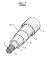
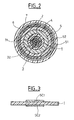
- the interior semiconductor screen 3 is a composite which comprises (see FIG. 2) a layer 31 of high longitudinal volumetric electrical conductivity, typically greater than 0.1 S / m between 20 and 90 ° C, and preferably greater than 5 S / m at these temperatures, in contact with the conductive core 1, and a layer 32 capable of injecting a small amount of space charges into the insulation layer 4 after polarization, so that the amount of space charges injected from the screen 3 in the electrical insulation layer 4 is typically less than 200 nC between 25 and 70 ° C, the layer 32 being in contact with the electrical insulation layer 4.
- the outer semiconductor screen 5 is a composite which comprises a layer 51 of high volume electrical conductivity, typically greater than 0.1 S / m between 20 and 90 ° C, and preferably greater than 5 S / m at these temperatures, the layer 51 being in contact with the metal screen 6, and a layer 52 capable of injecting a small amount of space charges into the insulation layer 4 after polarization, so that the amount of space charges injected from the screen 5 into the electrical insulation layer 4 is typically less than 200 nC between 25 and 70 ° C, the layer 52 being in contact with the electrical insulation layer 4.
- the semiconductor screens 3 and 5 according to the invention allow both to obtain a satisfactory electrical conductivity in the vicinity of the conductive elements of the cable 10 in order to perform the function of homogenizing the distribution of the field. electric, and to limit the injection of space charges into the electrical insulation layer 4 since the layers 32 and 52 of the semiconductor screens 3 and 5 in contact with the latter inject a small amount of space charges after polarization.
- Each of these samples comprises an electrically insulating layer I of thickness 0.8 mm placed between two semiconductor layers SC1 and SC2 of identical compositions.
- the two layers SC1 and SC2 are composite semiconductor screens according to the invention each consisting of a layer of a material of Composition 1 given below, capable of inducing a large amount of charges d space and a layer of a material of Composition 2 given below, inducing a small amount of space charges in the electrically insulating layer I with which it is in contact.
- the two layers SC1 and SC2 consist only of a material of Composition 2 above.
- the two layers SC1 and SC2 consist solely of a material of Composition 1 above.
- compositions 1 and 2 above were chosen in order to be able to carry out comparisons of quantities of space charges injected, and this independently of their electrical conductivity.
- the test implemented consists in sending the beam of a YAG laser onto the test sample, each semiconductor screen of which constitutes an electrode (+) and (-).
- This beam absorbed on the surface of the electrode (-) decomposes this surface by pyrolysis, and the gases emitted cause a pressure wave which crosses the sample, causing a displacement of space charges and the appearance of image charges at the electrodes. , giving rise to the measured signal.
- the processing of this signal gives an indication of the distribution of the electric field and of the volume charge density in the sample.
- Table 1 below gives the results obtained outside the applied field, after polarization of the samples for 4 hours under a continuous electrical voltage of +40 kV at room temperature (25 ° C).
- Table 1 Sample D + (C / m 3 ) D - (C / m 3 ) Q T (nC) AT 0,019 0.03 5 B 0.9 0.05 76 VS 1.8 0.5 98
- Table 2 gives the results obtained after polarization of the samples for 4 hours under a continuous electrical voltage of +40 kV at 70 ° C.
- Table 2 Sample D + (C / m 3 ) D - (C / m 3 ) Q T (nC) AT 0.15 0.19 48 B 1.1 0.6 126 VS 2.5 1.8 196
- Table 2 shows that the results obtained at room temperature are also valid at high temperature.
- the two layers SC1 and SC2 are composite semiconductor screens according to the invention each consisting of a layer of a material of Composition 3 given below, capable of inducing a large amount of charges d space, and a layer of a material of Composition 4 given below, inducing a small amount space charges in the electrically insulating layer I with which it is in contact.
- the two layers SC1 and SC2 consist only of a material of Composition 4 above.
- the two layers SC1 and SC2 consist only of a material of Composition 3 above
- the two layers SC1 and SC2 consist solely of a semiconductor material with high injection of space charges and high commercial electrical conductivity, based on a mixture of polyethylene and copolymer of ethylene and vinyl acetate.
- compositions 3 to 5 above have been chosen in order to be able to carry out comparisons of quantities of space charges injected, and this independently of their electrical conductivity.
- Table 3 gives the results obtained outside the applied field, after polarization of the samples for 4 hours under a continuous electrical voltage of +40 kV at room temperature (25 ° C).
- Table 3 Sample D + (C / m 3 ) D - (C / m 3 ) Q T (nC) D 0.09 0.04 5 E 1.05 0.21 43 F 1.95 0.69 80 G 1.68 0.85 235
- Table 4 gives the results obtained after polarization of the samples for 4 hours under a continuous electrical voltage of +40 kV at 70 ° C.
- Table 4 Sample D + (C / m 3 ) D - (C / m 3 ) Q T (nC) D 0.52 0.3 53 E 1.25 0.65 102 F 2.82 1.91 422 G 1.15 0.98 205
- a screen according to the invention can be obtained by co-extrusion of its two constituent layers in a suitable device, well known to those skilled in the art.
- an energy cable according to the invention may comprise only a semiconductor screen according to the invention, for example the interior semiconductor screen only or the exterior semiconductor screen only.
- the cable according to the invention may include other types of metallic protective screens, for example a laminated or welded aluminum screen.
- the protective structure which comprises the metal screen and the outer sheath may also include other protective elements such as in particular a swelling protective strip in the presence of water.
- a protective strip can be interposed between the outer semiconductor screen and the metal protective screen. It provides itself or is associated with conductive means ensuring electrical continuity between the outer semiconductor screen and the metal screen.
Landscapes
- Insulated Conductors (AREA)
- Conductive Materials (AREA)
- Communication Cables (AREA)
- Cable Accessories (AREA)
- Structures Or Materials For Encapsulating Or Coating Semiconductor Devices Or Solid State Devices (AREA)
- Organic Insulating Materials (AREA)
Applications Claiming Priority (2)
| Application Number | Priority Date | Filing Date | Title |
|---|---|---|---|
| FR0110045A FR2827999B1 (fr) | 2001-07-25 | 2001-07-25 | Ecran semi-conducteur pour cable d'energie |
| FR0110045 | 2001-07-25 |
Publications (2)
| Publication Number | Publication Date |
|---|---|
| EP1280167A1 true EP1280167A1 (de) | 2003-01-29 |
| EP1280167B1 EP1280167B1 (de) | 2009-01-07 |
Family
ID=8865972
Family Applications (1)
| Application Number | Title | Priority Date | Filing Date |
|---|---|---|---|
| EP02291796A Expired - Lifetime EP1280167B1 (de) | 2001-07-25 | 2002-07-17 | Halbleitende Abschirmung für Energiekabel |
Country Status (7)
| Country | Link |
|---|---|
| EP (1) | EP1280167B1 (de) |
| JP (1) | JP4630519B2 (de) |
| AT (1) | ATE420443T1 (de) |
| DE (1) | DE60230698D1 (de) |
| DK (1) | DK1280167T3 (de) |
| ES (1) | ES2320202T3 (de) |
| FR (1) | FR2827999B1 (de) |
Cited By (5)
| Publication number | Priority date | Publication date | Assignee | Title |
|---|---|---|---|---|
| US8361606B2 (en) * | 2004-07-02 | 2013-01-29 | Ticona Gmbh | Composite comprising at least one hard component and at least one soft component |
| CN103093868A (zh) * | 2013-01-28 | 2013-05-08 | 东莞市瀛通电线有限公司 | 合金填充抗拉耳机电线 |
| WO2013182829A1 (fr) * | 2012-06-08 | 2013-12-12 | Nexans | Dispositif comprenant une couche piégeuse de charges d'espace |
| CN103915201A (zh) * | 2013-09-25 | 2014-07-09 | 安徽省高沟电缆有限公司 | 一种石油化工用控制电力电缆 |
| CN107077918A (zh) * | 2014-10-17 | 2017-08-18 | 3M创新有限公司 | 具有增强的击穿强度的电介质材料 |
Families Citing this family (2)
| Publication number | Priority date | Publication date | Assignee | Title |
|---|---|---|---|---|
| KR101161360B1 (ko) * | 2010-07-13 | 2012-06-29 | 엘에스전선 주식회사 | 공간전하 저감 효과를 갖는 직류용 전력 케이블 |
| CN105023637B (zh) * | 2015-08-15 | 2017-05-31 | 国网新疆电力公司塔城供电公司 | 抗电磁干扰的高压电缆 |
Citations (2)
| Publication number | Priority date | Publication date | Assignee | Title |
|---|---|---|---|---|
| GB2165689A (en) * | 1984-10-08 | 1986-04-16 | Ass Elect Ind | High voltage cables |
| GB2252866A (en) * | 1991-01-03 | 1992-08-19 | Phillips Cables Ltd | Flexible electrically insulated electric conductor |
Family Cites Families (12)
| Publication number | Priority date | Publication date | Assignee | Title |
|---|---|---|---|---|
| JPS50116983A (de) * | 1974-02-28 | 1975-09-12 | ||
| JPS53137676U (de) * | 1977-04-05 | 1978-10-31 | ||
| JPS6063813A (ja) * | 1983-09-19 | 1985-04-12 | 日立電線株式会社 | 電力ケ−ブル用半導電性組成物 |
| JPS636707A (ja) * | 1986-06-27 | 1988-01-12 | 昭和電線電纜株式会社 | 架橋ポリオレフイン絶縁ケ−ブル |
| JPS6424307A (en) * | 1987-07-21 | 1989-01-26 | Fujikura Ltd | Dc power cable |
| JPS6424308A (en) * | 1987-07-21 | 1989-01-26 | Fujikura Ltd | Dc power cable |
| WO1992017995A1 (fr) * | 1991-04-02 | 1992-10-15 | Alcatel Cable | Materiau pour ecran semi-conducteur |
| FR2710183B3 (fr) * | 1993-09-17 | 1995-10-13 | Alcatel Cable | Câble d'énergie à rigidité diélectrique améliorée. |
| JPH08306243A (ja) * | 1995-05-08 | 1996-11-22 | Fujikura Ltd | 電力ケーブルと接続用テープ |
| JPH1079205A (ja) * | 1996-09-04 | 1998-03-24 | Fujikura Ltd | 電力ケーブルおよび電力機器 |
| JPH10255561A (ja) * | 1997-03-06 | 1998-09-25 | Showa Electric Wire & Cable Co Ltd | 直流電力ケーブル |
| JPH11260158A (ja) * | 1998-03-09 | 1999-09-24 | Showa Electric Wire & Cable Co Ltd | 直流電力ケーブル |
-
2001
- 2001-07-25 FR FR0110045A patent/FR2827999B1/fr not_active Expired - Fee Related
-
2002
- 2002-07-17 DK DK02291796T patent/DK1280167T3/da active
- 2002-07-17 EP EP02291796A patent/EP1280167B1/de not_active Expired - Lifetime
- 2002-07-17 AT AT02291796T patent/ATE420443T1/de not_active IP Right Cessation
- 2002-07-17 DE DE60230698T patent/DE60230698D1/de not_active Expired - Lifetime
- 2002-07-17 ES ES02291796T patent/ES2320202T3/es not_active Expired - Lifetime
- 2002-07-24 JP JP2002215399A patent/JP4630519B2/ja not_active Expired - Fee Related
Patent Citations (2)
| Publication number | Priority date | Publication date | Assignee | Title |
|---|---|---|---|---|
| GB2165689A (en) * | 1984-10-08 | 1986-04-16 | Ass Elect Ind | High voltage cables |
| GB2252866A (en) * | 1991-01-03 | 1992-08-19 | Phillips Cables Ltd | Flexible electrically insulated electric conductor |
Cited By (9)
| Publication number | Priority date | Publication date | Assignee | Title |
|---|---|---|---|---|
| US8361606B2 (en) * | 2004-07-02 | 2013-01-29 | Ticona Gmbh | Composite comprising at least one hard component and at least one soft component |
| WO2013182829A1 (fr) * | 2012-06-08 | 2013-12-12 | Nexans | Dispositif comprenant une couche piégeuse de charges d'espace |
| FR2991808A1 (fr) * | 2012-06-08 | 2013-12-13 | Nexans | Dispositif comprenant une couche piegeuse de charges d'espace |
| US9748758B2 (en) | 2012-06-08 | 2017-08-29 | Nexans | Device comprising a space charge trapping layer |
| CN103093868A (zh) * | 2013-01-28 | 2013-05-08 | 东莞市瀛通电线有限公司 | 合金填充抗拉耳机电线 |
| CN103915201A (zh) * | 2013-09-25 | 2014-07-09 | 安徽省高沟电缆有限公司 | 一种石油化工用控制电力电缆 |
| CN107077918A (zh) * | 2014-10-17 | 2017-08-18 | 3M创新有限公司 | 具有增强的击穿强度的电介质材料 |
| US20170250008A1 (en) * | 2014-10-17 | 2017-08-31 | 3M Innovative Properties Company | Dielectric material with enhanced breakdown strength |
| US10121570B2 (en) * | 2014-10-17 | 2018-11-06 | 3M Innovative Properties Company | Dielectric material with enhanced breakdown strength |
Also Published As
| Publication number | Publication date |
|---|---|
| DK1280167T3 (da) | 2009-05-04 |
| DE60230698D1 (de) | 2009-02-26 |
| ES2320202T3 (es) | 2009-05-20 |
| JP4630519B2 (ja) | 2011-02-09 |
| JP2003051218A (ja) | 2003-02-21 |
| FR2827999A1 (fr) | 2003-01-31 |
| FR2827999B1 (fr) | 2003-10-17 |
| EP1280167B1 (de) | 2009-01-07 |
| ATE420443T1 (de) | 2009-01-15 |
Similar Documents
| Publication | Publication Date | Title |
|---|---|---|
| EP1128395B1 (de) | Hoch und Höchstspannungsgleichstromenergiekabel | |
| EP2224459B1 (de) | Hochspannungskabel | |
| EP0068307B1 (de) | Elektrochemische Generatoren mit Festelektrolyten aus kationenleitenden glasartigen Verbindungen | |
| EP2483894A1 (de) | Mittel- oder hochspannungsstromkabel | |
| CA2521447A1 (en) | Electrical cables | |
| EP2765581B1 (de) | Elektrisches Kabel, das resistent gegen Teilentladungen ist | |
| EP0660483B1 (de) | Vorrichtung zum Verbinden von Energiekabeln | |
| EP1280167B1 (de) | Halbleitende Abschirmung für Energiekabel | |
| EP2136376B1 (de) | Hochspannungsstromkabel | |
| EP2498263B1 (de) | elektrische Hochspannungs- und mittelspannungskabel | |
| KR100323179B1 (ko) | 케이블절연구조 | |
| EP0645781B1 (de) | Energiekabel mit verbesserter dielektrischen Festigkeit | |
| EP3764372A1 (de) | Kabel, das eine feuerbeständige schicht umfasst | |
| EP2194092B1 (de) | Elektrisches Kabel | |
| WO2019086685A1 (fr) | Extremite de cable et procede de fabrication correspondant | |
| JPH103823A (ja) | 直流架橋ポリエチレン絶縁電力ケーブル | |
| EP2535901B1 (de) | Mittel- und Hochspannungsstromkabel mit einem Polyolefin-Schutzmantel, der mineralische Füllstoffe enthält | |
| EP2498264B1 (de) | Mittel- oder Hochspannungsstromkabel | |
| EP4092689A1 (de) | Elektrisches kabel, das teilentladungen begrenzt | |
| EP3671768A1 (de) | Elektrisches kabel, das beständig gegen wasserbäumchen ist | |
| FR2601184A1 (fr) | Cable electrique de securite resistant au feu et non-propagateur de l'incendie, ainsi que son procede de fabrication | |
| EP3544025A1 (de) | Elektrokabel mit einer leicht abziehbaren polymerschicht | |
| FR2654867A1 (fr) | Cable electrique apte a assurer un service electrique minimum pendant un incendie meme directement soumis a une flamme. | |
| FR2508239A2 (fr) | Generateurs electrochimiques utilisant une composition vitreuse conductrice de cations alcalins | |
| EP3503125A1 (de) | Kabel, das mindestens eine metallisierte schicht eines kohlenstoffmaterials umfasst |
Legal Events
| Date | Code | Title | Description |
|---|---|---|---|
| PUAI | Public reference made under article 153(3) epc to a published international application that has entered the european phase |
Free format text: ORIGINAL CODE: 0009012 |
|
| AK | Designated contracting states |
Designated state(s): AT BE BG CH CY CZ DE DK EE ES FI FR GB GR IE IT LI LU MC NL PT SE SK TR |
|
| AX | Request for extension of the european patent |
Extension state: AL LT LV MK RO SI |
|
| 17P | Request for examination filed |
Effective date: 20030729 |
|
| AKX | Designation fees paid |
Designated state(s): AT BE BG CH CY CZ DE DK EE ES FI FR GB GR IE IT LI LU MC NL PT SE SK TR |
|
| REG | Reference to a national code |
Ref country code: SE Ref legal event code: TRGR |
|
| GRAP | Despatch of communication of intention to grant a patent |
Free format text: ORIGINAL CODE: EPIDOSNIGR1 |
|
| GRAS | Grant fee paid |
Free format text: ORIGINAL CODE: EPIDOSNIGR3 |
|
| GRAA | (expected) grant |
Free format text: ORIGINAL CODE: 0009210 |
|
| AK | Designated contracting states |
Kind code of ref document: B1 Designated state(s): AT BE BG CH CY CZ DE DK EE ES FI FR GB GR IE IT LI LU MC NL PT SE SK TR |
|
| REG | Reference to a national code |
Ref country code: GB Ref legal event code: FG4D Free format text: NOT ENGLISH |
|
| REG | Reference to a national code |
Ref country code: CH Ref legal event code: EP |
|
| REG | Reference to a national code |
Ref country code: IE Ref legal event code: FG4D Free format text: LANGUAGE OF EP DOCUMENT: FRENCH |
|
| REF | Corresponds to: |
Ref document number: 60230698 Country of ref document: DE Date of ref document: 20090226 Kind code of ref document: P |
|
| REG | Reference to a national code |
Ref country code: DK Ref legal event code: T3 |
|
| REG | Reference to a national code |
Ref country code: ES Ref legal event code: FG2A Ref document number: 2320202 Country of ref document: ES Kind code of ref document: T3 |
|
| PG25 | Lapsed in a contracting state [announced via postgrant information from national office to epo] |
Ref country code: NL Free format text: LAPSE BECAUSE OF FAILURE TO SUBMIT A TRANSLATION OF THE DESCRIPTION OR TO PAY THE FEE WITHIN THE PRESCRIBED TIME-LIMIT Effective date: 20090107 |
|
| NLV1 | Nl: lapsed or annulled due to failure to fulfill the requirements of art. 29p and 29m of the patents act | ||
| PG25 | Lapsed in a contracting state [announced via postgrant information from national office to epo] |
Ref country code: FI Free format text: LAPSE BECAUSE OF FAILURE TO SUBMIT A TRANSLATION OF THE DESCRIPTION OR TO PAY THE FEE WITHIN THE PRESCRIBED TIME-LIMIT Effective date: 20090107 |
|
| REG | Reference to a national code |
Ref country code: IE Ref legal event code: FD4D |
|
| PG25 | Lapsed in a contracting state [announced via postgrant information from national office to epo] |
Ref country code: AT Free format text: LAPSE BECAUSE OF FAILURE TO SUBMIT A TRANSLATION OF THE DESCRIPTION OR TO PAY THE FEE WITHIN THE PRESCRIBED TIME-LIMIT Effective date: 20090107 Ref country code: PT Free format text: LAPSE BECAUSE OF FAILURE TO SUBMIT A TRANSLATION OF THE DESCRIPTION OR TO PAY THE FEE WITHIN THE PRESCRIBED TIME-LIMIT Effective date: 20090608 |
|
| PG25 | Lapsed in a contracting state [announced via postgrant information from national office to epo] |
Ref country code: EE Free format text: LAPSE BECAUSE OF FAILURE TO SUBMIT A TRANSLATION OF THE DESCRIPTION OR TO PAY THE FEE WITHIN THE PRESCRIBED TIME-LIMIT Effective date: 20090107 Ref country code: CZ Free format text: LAPSE BECAUSE OF FAILURE TO SUBMIT A TRANSLATION OF THE DESCRIPTION OR TO PAY THE FEE WITHIN THE PRESCRIBED TIME-LIMIT Effective date: 20090107 Ref country code: IE Free format text: LAPSE BECAUSE OF FAILURE TO SUBMIT A TRANSLATION OF THE DESCRIPTION OR TO PAY THE FEE WITHIN THE PRESCRIBED TIME-LIMIT Effective date: 20090107 |
|
| PLBE | No opposition filed within time limit |
Free format text: ORIGINAL CODE: 0009261 |
|
| STAA | Information on the status of an ep patent application or granted ep patent |
Free format text: STATUS: NO OPPOSITION FILED WITHIN TIME LIMIT |
|
| PG25 | Lapsed in a contracting state [announced via postgrant information from national office to epo] |
Ref country code: SK Free format text: LAPSE BECAUSE OF FAILURE TO SUBMIT A TRANSLATION OF THE DESCRIPTION OR TO PAY THE FEE WITHIN THE PRESCRIBED TIME-LIMIT Effective date: 20090107 |
|
| 26N | No opposition filed |
Effective date: 20091008 |
|
| PG25 | Lapsed in a contracting state [announced via postgrant information from national office to epo] |
Ref country code: BG Free format text: LAPSE BECAUSE OF FAILURE TO SUBMIT A TRANSLATION OF THE DESCRIPTION OR TO PAY THE FEE WITHIN THE PRESCRIBED TIME-LIMIT Effective date: 20090407 |
|
| BERE | Be: lapsed |
Owner name: NEXANS Effective date: 20090731 |
|
| PG25 | Lapsed in a contracting state [announced via postgrant information from national office to epo] |
Ref country code: MC Free format text: LAPSE BECAUSE OF NON-PAYMENT OF DUE FEES Effective date: 20090731 |
|
| PG25 | Lapsed in a contracting state [announced via postgrant information from national office to epo] |
Ref country code: BE Free format text: LAPSE BECAUSE OF NON-PAYMENT OF DUE FEES Effective date: 20090731 |
|
| PG25 | Lapsed in a contracting state [announced via postgrant information from national office to epo] |
Ref country code: GR Free format text: LAPSE BECAUSE OF FAILURE TO SUBMIT A TRANSLATION OF THE DESCRIPTION OR TO PAY THE FEE WITHIN THE PRESCRIBED TIME-LIMIT Effective date: 20090408 |
|
| PG25 | Lapsed in a contracting state [announced via postgrant information from national office to epo] |
Ref country code: LU Free format text: LAPSE BECAUSE OF NON-PAYMENT OF DUE FEES Effective date: 20090717 |
|
| PG25 | Lapsed in a contracting state [announced via postgrant information from national office to epo] |
Ref country code: TR Free format text: LAPSE BECAUSE OF FAILURE TO SUBMIT A TRANSLATION OF THE DESCRIPTION OR TO PAY THE FEE WITHIN THE PRESCRIBED TIME-LIMIT Effective date: 20090107 |
|
| PG25 | Lapsed in a contracting state [announced via postgrant information from national office to epo] |
Ref country code: CY Free format text: LAPSE BECAUSE OF FAILURE TO SUBMIT A TRANSLATION OF THE DESCRIPTION OR TO PAY THE FEE WITHIN THE PRESCRIBED TIME-LIMIT Effective date: 20090107 |
|
| PGFP | Annual fee paid to national office [announced via postgrant information from national office to epo] |
Ref country code: ES Payment date: 20110726 Year of fee payment: 10 |
|
| REG | Reference to a national code |
Ref country code: ES Ref legal event code: FD2A Effective date: 20131021 |
|
| PG25 | Lapsed in a contracting state [announced via postgrant information from national office to epo] |
Ref country code: ES Free format text: LAPSE BECAUSE OF NON-PAYMENT OF DUE FEES Effective date: 20120718 |
|
| PGFP | Annual fee paid to national office [announced via postgrant information from national office to epo] |
Ref country code: CH Payment date: 20130719 Year of fee payment: 12 Ref country code: DK Payment date: 20130719 Year of fee payment: 12 |
|
| PGFP | Annual fee paid to national office [announced via postgrant information from national office to epo] |
Ref country code: GB Payment date: 20130719 Year of fee payment: 12 |
|
| REG | Reference to a national code |
Ref country code: DK Ref legal event code: EBP Effective date: 20140731 |
|
| REG | Reference to a national code |
Ref country code: CH Ref legal event code: PL |
|
| GBPC | Gb: european patent ceased through non-payment of renewal fee |
Effective date: 20140717 |
|
| PG25 | Lapsed in a contracting state [announced via postgrant information from national office to epo] |
Ref country code: CH Free format text: LAPSE BECAUSE OF NON-PAYMENT OF DUE FEES Effective date: 20140731 Ref country code: LI Free format text: LAPSE BECAUSE OF NON-PAYMENT OF DUE FEES Effective date: 20140731 |
|
| PG25 | Lapsed in a contracting state [announced via postgrant information from national office to epo] |
Ref country code: GB Free format text: LAPSE BECAUSE OF NON-PAYMENT OF DUE FEES Effective date: 20140717 |
|
| REG | Reference to a national code |
Ref country code: FR Ref legal event code: PLFP Year of fee payment: 14 |
|
| PG25 | Lapsed in a contracting state [announced via postgrant information from national office to epo] |
Ref country code: DK Free format text: LAPSE BECAUSE OF NON-PAYMENT OF DUE FEES Effective date: 20140731 |
|
| PGFP | Annual fee paid to national office [announced via postgrant information from national office to epo] |
Ref country code: FR Payment date: 20150626 Year of fee payment: 14 |
|
| PGFP | Annual fee paid to national office [announced via postgrant information from national office to epo] |
Ref country code: DE Payment date: 20150721 Year of fee payment: 14 |
|
| PGFP | Annual fee paid to national office [announced via postgrant information from national office to epo] |
Ref country code: SE Payment date: 20150721 Year of fee payment: 14 |
|
| PGFP | Annual fee paid to national office [announced via postgrant information from national office to epo] |
Ref country code: IT Payment date: 20150727 Year of fee payment: 14 |
|
| REG | Reference to a national code |
Ref country code: DE Ref legal event code: R119 Ref document number: 60230698 Country of ref document: DE |
|
| REG | Reference to a national code |
Ref country code: SE Ref legal event code: EUG |
|
| PG25 | Lapsed in a contracting state [announced via postgrant information from national office to epo] |
Ref country code: DE Free format text: LAPSE BECAUSE OF NON-PAYMENT OF DUE FEES Effective date: 20170201 Ref country code: FR Free format text: LAPSE BECAUSE OF NON-PAYMENT OF DUE FEES Effective date: 20160801 Ref country code: SE Free format text: LAPSE BECAUSE OF NON-PAYMENT OF DUE FEES Effective date: 20160718 |
|
| REG | Reference to a national code |
Ref country code: FR Ref legal event code: ST Effective date: 20170331 |
|
| PG25 | Lapsed in a contracting state [announced via postgrant information from national office to epo] |
Ref country code: IT Free format text: LAPSE BECAUSE OF NON-PAYMENT OF DUE FEES Effective date: 20160717 |