EP1276024A2 - Elektronischer Schaltkreis und Uhrwerk enthaltend einen solchen Schaltkreis - Google Patents
Elektronischer Schaltkreis und Uhrwerk enthaltend einen solchen Schaltkreis Download PDFInfo
- Publication number
- EP1276024A2 EP1276024A2 EP02022189A EP02022189A EP1276024A2 EP 1276024 A2 EP1276024 A2 EP 1276024A2 EP 02022189 A EP02022189 A EP 02022189A EP 02022189 A EP02022189 A EP 02022189A EP 1276024 A2 EP1276024 A2 EP 1276024A2
- Authority
- EP
- European Patent Office
- Prior art keywords
- signal
- energy dissipation
- electronic circuit
- circuit
- circuit according
- Prior art date
- Legal status (The legal status is an assumption and is not a legal conclusion. Google has not performed a legal analysis and makes no representation as to the accuracy of the status listed.)
- Granted
Links
Images



Classifications
-
- G—PHYSICS
- G04—HOROLOGY
- G04C—ELECTROMECHANICAL CLOCKS OR WATCHES
- G04C19/00—Producing optical time signals at prefixed times by electric means
-
- G—PHYSICS
- G04—HOROLOGY
- G04C—ELECTROMECHANICAL CLOCKS OR WATCHES
- G04C10/00—Arrangements of electric power supplies in time-pieces
-
- G—PHYSICS
- G04—HOROLOGY
- G04G—ELECTRONIC TIME-PIECES
- G04G19/00—Electric power supply circuits specially adapted for use in electronic time-pieces
-
- G—PHYSICS
- G04—HOROLOGY
- G04C—ELECTROMECHANICAL CLOCKS OR WATCHES
- G04C11/00—Synchronisation of independently-driven clocks
Definitions
- the present invention relates to an electronic Circuit according to the preamble of claim 1 and a Clockwork that contains such a circuit.
- CH-A-597636 (Ebauches S.A.) proposed the batteries a clockwork by a generator and a generator to replace the driving spring.
- the movement described contains one Spring, a time display and a one over a gear train Drives AC generator.
- the generator feeds a rectifier, the rectifier feeds a capacitive component, and the capacitive component feeds an electronic reference circuit with a stable crystal oscillator as well as an electronic one Control circuit.
- the electronic control circuit has a comparator logic circuit and one with the output of the comparator logic circuit connected and through the comparator logic circuit in their Power consumption controllable energy dissipation circuit.
- On Input of the comparator logic circuit is electronic Reference circuit and another input of the comparator logic circuit is connected to the generator.
- the comparator logic circuit is designed to be one of the most electronic Reference circuit coming clock signal with a from the generator originating clock signal compares, depending on the result of this Compare the size of the power consumption of the Energy dissipation circuit controls and in this way via the Control the control circuit power consumption the gear of Generator and thus regulates the course of the time display.
- Patent documents EP-A-0239820 and EP-A-679968 describe various electronic circuits for controlling the Speed of one of the microgenerators in which one Monitoring circuit constantly monitors the angular position of the rotor and brakes it as soon as its angular position is ahead. These circuits because of their sensitivity to errors and phase variations Components, difficult to handle.
- the voltage converter circuit contains several Capacities C1; C2; C3, which is from the microgenerator through active elements are fed, for example by field effect transistors instead of Diodes. Diodes are only used to initialize the system. The energetic efficiency of the circuit can be strong in this way be improved by the threshold voltage losses of the diodes be avoided. The circuit can thus have a lower Peak voltage work, which reduces the size of the Generator and the spring and an increase in the power reserve of the Clockwork allowed.
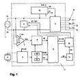
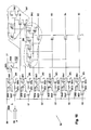
- FIG 1 is a block diagram of an inventive electronic circuit 11 for speed control of a Microgenerators shown.
- the electronic circuit is from Microgenerator 1, the speed of which it regulates, via a capacitance C3, which temporarily stores the energy given off by the generator, fed.
- the microgenerator 1, which generates an alternating voltage, is via a gear train, not shown, from a train, not shown Spring driven.
- the gear train also drives the time display (not shown).
- the electronic circuit 11 regulates the Power consumption of one connected to the microgenerator Energy dissipation circuit 9 (Fig. 11) so that the rotation frequency of the Rotor of the microgenerator with the reference frequency at the output of a Frequency divider 5, the input of which is fed by a quartz oscillator 3, 4 is synchronized.
- a microgenerator is used, which is described in patent application EP-A-851332.
- the nominal frequency of the alternating voltage of the microgenerator 1 is preferably 2 n Hz, where n is a natural number different from zero.
- the mechanical part of the clockwork is part of the prior art and is described, for example, in CH-A-597636.
- the microgenerator 1 has the two inputs G- and G + of the electronic circuit 11 connected.
- the circuit 11 is preferably constructed as a single IC.
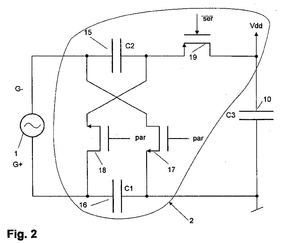
- the inputs are G- and G + connected to a rectification and voltage converter circuit 2, the Function is described below with reference to Figures 2-5.
- the Rectifier and voltage converter 2 charges a storage capacitor 10 (C3), which temporarily stores the electrical energy generated by the Microgenerator is generated and gives the energy in the form of an im essential continuous voltage to the IC.
- the rectifier and voltage converter 2 uses two others Capacitors 16 (C1) and 15 (C2).
- the capacitors are C1, C2 and C3 preferably external, although they are also integrated in the IC 11 could.
- the energy dissipation circuit is connected in parallel with the microgenerator 1.
- the Energy dissipation circuit 9 could also be on the other side from the rectifier and voltage converter 2, in parallel with the capacitor C3 switched, arranged.
- the energy dissipation circuit 9 exists from an ohmic resistor, the value of which by energy dissipation control means 30 (Fig. 10) is controlled.
- the energy dissipation circuit 9 could also consist of an adjustable power source. The Rotation speed of the rotor of the microgenerator 1 is thereby controlled by varying the resistance value.
- a stabilized one, in particular with reference to FIG. 6 current source 32 described generates various stabilized currents pp, pn, which is used to feed the rectifier and voltage converter 2 and of elements 3, 7, 31 are determined.
- the stabilized power source 32 gets its energy from the capacitance C3, which feeds the entire IC.
- On Oscillator 3, 4 delivers a reference signal with a predetermined frequency.
- the oscillator 3, 4 has a quartz 4, which is preferably outside of the IC 11 is mounted and its vibrations a reference frequency define at the output of the oscillator 3. This reference frequency will divided by a predetermined factor by means of a frequency divider 5, which in detail with reference to FIGS. 7 and 8 is described.
- the IC also includes a counter 6, which in detail will be described with reference to Figure 9.
- Decrementing input (DOWN) of counter 6 is connected to the output of the Frequency divider 5 connected during the increment input (UP) the counter 6 via a hysteresis comparator 7, which the Determines zero transitions of the signal at the output of the microgenerator 1, and via an anti-coincidence circuit 8 with the microgenerator 1 connected is.
- the anti-coincidence circuit 8 prevents one simultaneous arrival of UP and DOWN pulses on both Inputs of counter 6, which would otherwise be unpredictable Can assume behavior.
- the Anti-coincidence circuit the signals UP and DOWN on signals with different phase, which come from the frequency divider 5.
- the IC further includes an internal voltage doubler 31, which it allowed the energy dissipation control means brake control 30 and Energy dissipation circuit 9 with a higher voltage HV> Vdd and to feed and control a lower voltage LV ⁇ Vss.
- the energy dissipation control means 30 control the Energy dissipation of the energy dissipation circuit 9 as a function of Reference signal, which is generated by the quartz crystal 3.4 and from Signal that comes from the microgenerator 1. If the rotor of the Microgenerator 1 rotates too fast, the frequency of the signal is between the inputs G + and G- greater than the frequency of the reference signal on Output of the frequency divider 5. The counter 6 thus receives during one Time interval more pulses on its incremental input UP than on its decrement input DOWN; its count thus increases. The energy dissipation control means 30 control this function the resistance value from the energy dissipation circuit 9 and consequently the energy dissipation in such a way that the Microgenerator 1 is braked. In this way the rotational frequency of the microgenerator 1, and thus also the course of the time display with the Reference frequency, which comes from the crystal oscillator, synchronized.
- the regulation value B1: B31 which of the Energy dissipation circuit 9 from the energy dissipation control means 30 in this example depends on the counter value 6, that is from the difference in the number of pulses of the signal UP, which of the Microgenerator come, and the number of pulses DOWN, which from Fourth oscillator 3.4 has been coming since the clock was started.
- the type of control is therefore integral.
- Other types of regulation for example one Regulation, which is proportional to the current frequency difference or to the gradient of the frequency difference or a PID control (Proportionally-integral-derived) can also be used.
- the rotor speed of rotation regulated by the braking resistance value in the Energy dissipation circuit 9 is regulated; an on, off regulation but could also be used.
- the energy dissipation control means include a hysteresis comparator 7, which the signals G +, G- on the two inputs connected to the microgenerator 1.
- the signal Gen at the output of the comparator 7 is thus a rectangular signal, which changes its state every time the signal changes polarity the inputs G +, G- changes.
- the use of a Hysteresis comparator allows filtering of signal disturbances between the inputs G +, G-. To avoid unwanted Changes in the value of the signal Gen, which lead to incorrect Increments and thus excessive braking of the Microgenerators could lead to other filter media, for example a low pass or band filter, or a filter that only after one predefined time period changes its state, are provided.
- the Hysteresis comparator 7 is fed by the current source 32.
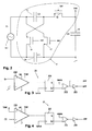
- the rectification and voltage converter circuit 2 is on the Figures 2-5 shown.
- the first switch 19 preferably consists of a Field effect transistor, which immediately after starting the clockwork acts as a simple diode.
- the voltage drop across the switch 19 is in this moment equal to the diode threshold voltage, about 400 mV.
- the transistors that act as switches through the Controlled comparators are the transistors that act as switches through the Controlled comparators. If that of the Voltage triple circuit voltage is higher than that Voltage of the capacitor 10, the first field effect transistor open. The voltage drop across the channel of the field effect transistor however, is only about 10 mV. The loss of voltage is at the Using transistors and controlling the transistors Comparators instead of diodes are therefore significantly reduced The clockwork's energy reserve is used more economically and the power reserve elevated.
- the field effect transistor 19 is only blocked again when the voltage C2 supplied by the voltage tripler circuit again drops below the voltage Vdd of the first capacitor 10.
- the first switch 19 is controlled by a signal / ser, which from a first comparator circuit 21 shown in FIG. 4 is delivered.
- the comparator circuit 21 has a comparator 210, which compares the voltage on both sides of the switch 19. If the voltage C2 on the left side of the switch is higher than that Voltage Vdd on the right side, the output of the comparator goes 210 from 0 to 1.
- the offset voltage is + 2mV
- the Voltage difference across the switch 19 is 2mV or more, so that the output of the comparator 210 goes to 1.
- the switch 19 is blocked by the signal mess and this enables the comparator to measure the voltage difference to detect via the switch. Then the value at the output of the Comparator 210 in the blocked transistor 19 by means of a signal latch stored in a memory element 211. Only after a period of time the signals measuring and latch go to 0, and the switch 19 is switched to in the memory element 211 stored value ser driven. To this This ensures that the system does not vibrate and that the Current flows from C2 to Vdd.
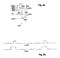
- a NAND gate 3081 which the frequency divider 5 emitted signals of 16 kHz, 8 kHz, 4 kHz, 2 kHz and 1 kHz combined, emits a signal p.
- the pulsation signal p therefore always has the Value 1, except once per 1 kHz cycle during a 16 kHz half cycle.
- This signal at the output of NAND gate 3081 is through an inverter 3082 which is connected to an AND gate 3083, inverted.
- a power-on-reset signal rudder the formation of which will be referred later 8 is explained at the other entrance to gate 3083 issued.
- the signal rud is zero, thereafter always one. So the signal is mess, which through gate 3083 delivered, always zero, except after starting when p has the logical state 1.
- the signal p at the output of the NAND gate 3081 is below other to the OR gate 3084, which also has a 32 kHz signal receives, which comes from the frequency divider 5.
- the signal r coming from the gate 3084 is always set to zero, except when p and the 32 kHz signal are zero at the same time, i.e. once per 1 kHz cycle during half a 32 kHz cycle.
- This Signal is validated by the signal rud and by means of a NAND gate 3085 inverted. So goes the signal latch, which through gate 3085 is only passed at zero if r has taken the value 1 and if rud is not zero at the same time.
- the signal latch is like this used to the state at the output of the comparators 20 and 21 in registers 201, 211 in the comparison circuits 20, 21.
- the voltage tripler 15, 16, 17, 18 contains a second one Capacitor 15 (C2) and a third capacitor 16 (C1) in series are connected to the inputs G + and G- with the microgenerator 1.
- a second switch 17 is connected between the input G and the Ground set end of the third capacitor 16 relative to the Micro generator switched.
- a third switch 18 is between the Input G + and the end of the second capacitor 15 opposite the Switched microgenerator, which is connected to the first switch 19 is.
- the switches 17 and 18 are switched by a second comparator circuit 20 ( Figure 3) controlled, which the electrical potential of the input G-, which is connected to the second capacitor 15, with the potential compares the mass.
- the switches 17 and 18 also consist of Field effect transistors, which act as diodes in the blocked state.
- the capacities 15 and 16 charged through the diode structures of transistors 17 and 18.
- the second comparator circuit 20 tilts at next edge of the signal mess, and the state of the comparator is stored in the memory element 201 at the edge of the latch signal, and the switches are controlled with the stored values.
- the two Transistors 15 and 16 are then conductive. Capacitors 15 and 16 are therefore only through the channel of transistors 17 and 18th charged, which turns out to be energetically favorable. It should be noted that the input G- connected to the microgenerator 1 via the channel of the Transistor 17 is set to ground as soon as transistor 17 conducts.
- Comparators 200 and 210 are used fed with the voltage Vdd stored in the capacitor C3. in the further you need a power supply pp, or pn, which by the current source 32, which is illustrated in Figure 6, is accomplished.
- the comparators do not work as long as the Currents pp and pn are not sufficiently high; in this case you stay Output in the zero state, such that the controlled switches 17, 18, 19 remain locked.
- the current source 32 consists of a classic current mirror. It contains a high value resistor 321, for example 300K ⁇ , which is between the ground and the source of an N-channel field effect transistor 322 is switched.
- the drain of transistor 322 is with the drain of the field effect transistor 323a and with the gate of 3 P-channel transistors 323a, 323b, 323c connected in series, the source of the latter fed with the voltage generated by the voltage converter 2 becomes.
- the drain of transistor 322 is further connected to the gate of the three P-channel field effect transistors 323a, 323b, 323c as a mirror circuit connected.
- the current pp which is the channel of transistor 322 and the Crossing resistor 321 feeds the comparator 200, which in FIG. 3 is explained.
- the drain of transistor 323a is with the drain of the N-channel transistor 322 connected and to the gate of the N-channel transistors 322a ', 322b', 322c ', 322d' in series and as a mirror with respect to transistor 322 connected.
- the source of transistor 322a ' is connected to ground.
- the current pn which crosses the transistors 323a ', 323b' and 323c ' feeds the comparator 210, which is explained in FIG. 4
- a decrease in pp leads to a reduction of voltage drop across resistor 323 and consequently to one Voltage reduction applied to the gate of P-channel transistors 323a ', 323b ', 323c' is created.
- these become more permeable, leading to leads to an increase in the voltage at the drain of transistor 323a ', which transistor 322 is applied to the gate.
- This becomes accordingly more permeable and allows an increase in the current flowing pp.
- the current pp is stabilized and therefore depends only slightly on the applied load. It is easy to show that the current pn which transistors 323a ', 323b' and 323c 'penetrate in the same way is stabilized.
- the size of the current can therefore be determined by the characteristics of the elements in the power source, particularly the Number of transistors and the size of their channels. It is as possible, the currents pp and pn through the two branches of the Mirror to determine freely.
- Such a current mirror has two equilibrium states. The first has been described and is achieved when the flows pp and pn have reached the desired strength. The second state corresponds the currents pp and pn equal to zero. This second state is by name reached when all transistors are blocked. This state exists especially when the system is energized, after which consequently the currents pp and pn are zero.
- An N-channel initialization transistor 320 is provided to one during the start-up phase To force current through the current mirror 32 so that it is its first Equilibrium reached. The gate of transistor 320 is on the Ground, while its source with the input G- of the microgenerator 1 connected is. The drain of the initialization transistor is connected to the gate of the P-channel transistors connected.
- the Output signal of the comparator circuit 20 changes its state as indicated in Figure 2 when the voltage at node G- lower than Vss and opens transistors 17 and 18, which input G- des Microgenerator 1 with the mass and input G + of the microgenerator connects to C2. As soon as the input G- is connected to ground, transistor 320 turns off and stops consuming current from now on. The current source 2 is initialized from now on and the currents pp and pn quickly reach the desired value.
- the power source can be easily completed for example by means of other N-channel transistors, the gate of which with the The drain of transistor 323a 'and the source are connected to ground.
- the current through these transistors can thus easily be used for the supply of other components are checked, for example by Components of the quartz oscillator 3.4.
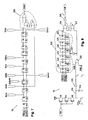
- FIG. 7 illustrates a preferred embodiment of a frequency divider 50 of the present invention.
- the frequency divider consists of ten D flip-flops connected in series. The frequency of the signal is divided by 2 for each flip-flop. If the reference signal supplied by the oscillator 3, 4 at the input of the frequency divider 50 oscillates at 32 kHz, the frequency of the signal at the output of the divider 50 2 -10 * 32kHz, that is 32 Hz. This signal is combined by the circuit 500 with the 4 kHz signal to produce a signal DOWN, which occurs once per cycle of 32 Hz and during a half cycle of 4kHz. assumes the logical state 1.
- FIG. 8 explains a circuit 51 that performs a power-on reset Signal rud delivers. This signal is determined, among other things, to Counter 6 at the initialization to a predetermined value reset and turn off the energy dissipation circuit 9.
- the Circuit 51 includes 3 P-channel field effect transistors 510, 511, 512, which is in series with a P-channel transistor between ground and the Supply are arranged. The gate of the three P-channel transistors is preserved the signal pp, which comes from the current source 32. In the Initialization the 3 transistors 510, 511 and 512 remain blocked, as long as the current source 32 does not provide sufficient current. The Voltage at point 516 is therefore zero.
- Inverter 550 converts this voltage into a signal POR1, which is generated by means of an OR gate 528 is combined with a signal POR2.
- the signal at the exit of the gate 528 is connected to one of the two NOR gates 517 and 518 Forwarded flip-flops with 2 inputs.
- the other input of the flip-flop 517, 518 is connected to the output of a frequency divider 520, which is composed of five flip-flops 521-526.
- the 32 Hz output signal, that is output by the frequency divider 50 is with connected to the input of the first flip-flop 521.
- the inputs / reset for The flip-flops 521-526 are reset via an inverter 527 with the Output of inverter 515 connected.
- the POR1 signal is one as long as the Power source does not provide enough power.
- that is Signal POR2 one as long as the frequency from the frequency divider 5 is not reaches a predetermined value.
- the signal at the exit of gate 528 is therefore only zero when the quartz oscillator and the Power source both work.
- this signal is still 1, so the Flip-flops 521-526 are all set to zero.
- the input of the flip-flop 517,518, which is connected to the flip-flop 526, thus receives the logic State zero while the input is connected to inverter 515 is connected, receives the logic state 1.
- the output of the flip-flop 517, 518 is therefore 1.
- the signal is inverted by the inverter 519 into a signal called rud (reset up-down counter) and has a logical value of zero.
- the 3rd Transistors 510 to 512 transparent.
- the signal at point 516 is consequently Vdd such that the inverter 515 outputs a signal POR1 with a returns logical value zero.
- the crystal oscillator works too, becomes a logic value zero at the flip-flop with 2 inputs 517, 518 through gate 528 while inputs / reset the flip-flop 521 - 526 receive the logical value 1.
- the frequency divider 520 begins with the division of the supplied 32 Hz frequency. After a second it works Signal at the output of the flip-flop 560 to 1. Since the two inputs of the If flip-flops 517, 518 receive the logical value 1, its output goes on Zero so that the signal rud reaches logic 1. This value will then maintain as long as the current value pp is sufficient and the crystal oscillator also works.
- the second power-on-reset signal POR2 goes to one as soon as the Frequency from the frequency divider drops below a certain value. After a short period of time, the signal rud reappears, so that the switches 17, 18, 19 of the voltage converter also in this case directly are controlled by the comparators 200, 210.
- the start-up of the IC is only ensured with the signal POR2 from the frequency divider.
- the Signal POR2 remains at zero.
- Figure 9 illustrates a preferred one Embodiment of the counter circuit 6.
- the Counter circuit 6 a 6-bit counter 60t.
- the counter 60 becomes, for example formed by six resettable D-series flip-flops.
- the binary number, which is formed by the outputs Q1 to Q6, takes by one unit on each leading edge, which is connected to input 601 is delivered to.
- the counter is reset to zero when a Signal rud is given to the reset input 603.
- the signals Q1 - Q6, which are output by the counter 6 allow the coding of 64 different braking values.
- the energy dissipation via the braking resistor Rf the Energy dissipation circuit 9 preferably develops in such Way as this is shown schematically on the diagram of Figure 10A is. Between 0 and 31 is the frequency difference integrated by counter 6 between the microgenerator 1 and the oscillator 3, 4 low: it becomes no braking initiated.
- FIG. 10 explains the energy dissipation control means 30 convert the signals Q1: Q6 from the counter into signals B1: B63, which the Drive energy dissipation circuit 9 explained in FIG. 11 directly.
- the energy dissipation circuit 9 directly connected between the inputs G +, G- of the microgenerator. she consists of a plurality of resistors 910 integrated on the IC to 916.
- the switches 900 to 906, which are replaced by the Energy dissipation control means 30 originating signals B1 to B5 and B62, B63 are controlled, allow a modification of the number of resistors arranged in parallel.
- the values of resistors 910 to According to FIG. 10A, 916 are inversely proportional to the strength of the Control signals B1 - B63: the signals B62 and B63 thus control a more effective one Braking as for example the signal B1.
- the switches 900 to 906 are N-channel field effect transistors. If the voltage at the gate of the transistor is at 0, the transistor blocks, so no current flows through the transistor. But as soon as the tension is on the source of the corresponding transistor is below Vss, the transistor becomes conductive. This means that the generator is braked because now a Current flows because the resistances between the terminals (G + and G-) of the Generator are switched.
- the Generator Depending on the circuit used, it is essential that the Generator a much higher speed than the nominal speed and thus achieved the highest possible output voltage so that the Circuit can start at all. However, it is possible that the The voltage at G + and G- is below Vss, so that the Generator is braked because the switching transistor for the brake is conductive becomes. But if the high speed and thus the high Output voltage is not reached, the circuit may fail because of the Do not start voltage drop across the diodes.
- the generator does not stop when the system is started is braked by the energy dissipation circuit 9, it is necessary at least one P-channel field effect transistors and at least one N-channel Field effect transistors switch in series when used as switches should serve to switch braking resistors between G + and G-.
- This is solved according to the invention with the P-channel field effect transistor 920.
- the P-channel field effect transistor 920 can only conduct when the voltage at the gate is lower than a threshold below the source voltage. At the Starting up the system is certainly not the case, so the generator is not braked and the system can be started.
- N-channel and P-channel transistors can only be close to Vss and Vdd can be used as good switches.
- Vss When the tension is on Drain and source somewhere between Vdd and Vss, it is not enough more, the gate with Vdd resp. Vss to drive the transistors become a leader.
- transistor 920 is not controlled with Vss, but rather with a signal LV, which is a much lower one in the active state Has voltage than Vss.
- LV is a much lower one in the active state Has voltage than Vss.
- the N-channel transistors 900: 906 cannot directly use the signals Q1: Q6 are driven from the counter because these Signals cannot be higher than Vdd. That's why they are Controlled transistors with the signals B1: B63, their logic states correspond to those of Q1: Q6, but their voltages doubled are.
- switch 18 of the Voltage converter 2 driven with a signal that the same logical state is like the signal par, but the voltage is increased. It would also be possible to par and ser the voltage of the signals that the Activate switches 17 and 19 to double.
- the level shifters 301-305 in Figure 10 are by a voltage HV fed, which by doubling the voltage Vdd on Capacitor C3 by means of a voltage doubler 31, not shown is obtained. So that the circuit can start reliably, the Voltage doubler can be built so that it also during initialization provides a voltage that is at least equal to Vdd. For that can Example of the voltage doubler 31 by the signal already described rud be driven so that it has a voltage during initialization Vdd delivers, and a doubled voltage HV only after the signal rud has changed its state when the crystal oscillator and the Power source both work.
- the logical state «62» is represented by an AND gate 306 proven when signals B2, B3, B4 and B5 are all 1 (62 expressed in decimal corresponds to 111110 binary).
- Gate 306 multiplies that Signals B2 to B5 and delivers a signal B62 with the logic state 1 only if the counter value reaches level 30 or 31.
- a second AND gate multiplies B62 by B1 in such a way that the logical state «63» is detected by means of a signal B63.
- the signals B62 or B63, directly control transistors 905 and 906.
- the circuit 30 supplies the signal LV, which for driving the P-channel transistor 920 in the Energy dissipation circuit 9 is determined.
- the LV signal is from one Levelshifter 300 generated.
- the voltage from the LV signal in the active state be at least one threshold lower than Vss.
- On Transistor 3006, which works like a diode, is between the other Side of capacity 3005 and the point / rud connected.
- the transistor 3006 has a threshold Ue, e.g. 400mV. If the level shifter 300 one Provides voltage HV, the voltage charged in the capacitance 3005 ⁇ U HV-Ue. When the voltage at the output of the level shifter 300 suddenly drops to Vss, the voltage of the LV signal drops to Vss- (HV-Ue) what allows transistor 920 to turn on.
- the signal / rud is one, see above LV remains at one and transistor 920 is turned off.
- the Transistor 920 can only conduct once the signal is rud / zero.
- the level shifter 300 is controlled by a signal / b, such that the energy dissipation circuit 9 brakes when the signal / b is zero is.
- the signal / b is emitted by a NAND gate 3080 which the signals Q6 and p logically combined.
- the signal / b is 1 if at least one of these two signals is zero. For example if Q6 Is zero, that is, if the counter 6 is not at least level 16 has reached, the signal / b is 1 such that the Energy dissipation circuit 9 can only brake from level 16 of the meter, according to the diagram of Fig. 10a.
- the formation of the pulsation signal p circuit 308 has already been used to explain FIG. 5a.
- the pulsation signal p therefore always has the value 1, except once per 1 kHz cycle during a 16 kHz half cycle. This serves to recharge the capacity that the LV generates.
Landscapes
- Physics & Mathematics (AREA)
- General Physics & Mathematics (AREA)
- Engineering & Computer Science (AREA)
- Power Engineering (AREA)
- Dc-Dc Converters (AREA)
- Electromechanical Clocks (AREA)
- Electric Clocks (AREA)
- Control Of Eletrric Generators (AREA)
- Control Of Electric Motors In General (AREA)
Abstract
Description
2-10*32kHz, das heisst 32 Hz. Dieses Signal wird durch den Schaltkreis 500 mit dem 4 kHz-Signal kombiniert, um ein Signal DOWN zu erzeugen, welches ein einziges Mal pro Zyklus von 32 Hz und während einem Halbzyklus von 4kHz. den logischen Zustand 1 annimmt.
Claims (26)
- Elektronischer Schaltkreis zur Regelung der Rotationsgeschwindigkeit eines Mikrogenerators (1) enthaltend:mindestens eine Steuerschaltung (20; 21) des oder der genannten Schalter (17, 18, 19), um die Spannung auf beiden Seiten des oder der genannten Schalter (17, 18, 19) zu vergleichen,einen ersten Eingang (G-) und einen zweiten Eingang (G+), die mit dem Mikrogenerator (1) verbunden werden können,einen Oszillator (3, 4) welcher ein Referenzsignal einer vorbestimmten Frequenz abgibt,eine Energiedissipationsschaltung (9) zur Bremsung des Mikrogenerators (9),Energiedissipationssteuermittel (5, 6, 7, 8, 30, 31) zur Steuerung der Energiedissipation der Energiedissipationsschaltung (9) in Abhängigkeit des Referenzsignals und des Signals zwischen den genannten Eingängen (G-, G+),eine Gleichricht- und Spannungswandlerschaltung (2) zur Gleichrichtung und Vervielfachung des Signals zwischen den genannten ersten und zweiten Eingängen, wobei die Gleichricht- und Spannungswandlerschaltung mindestens einen Kondensator (C1; C2; C3) enthält, welcher durch den genannten Mikrogenerator über mindestens einen Schalter (17, 18, 19) aufgeladen werden kann,
wobei der Ausgang der benannten Steuerschaltung zeitlich verzögert zur Ansteuerung des oder der genannten Schalter (17, 18, 19) verwendet wird. - Elektronischer Schaltkreis zur Regelung der Rotationsgeschwindigkeit eines Mikrogenerators (1) enthaltend:eine Gleichricht- und Spannungswandlerschaltung (2) zur Gleichrichtung und Vervielfachung des Signals zwischen den genannten ersten und zweiten Eingängen,einen ersten Eingang (G-) und einen zweiten Eingang (G+), die mit dem Mikrogenerator (1) verbunden werden können,einen Oszillator (3, 4) welcher ein Referenzsignal einer vorbestimmten Frequenz abgibt,eine Energiedissipationsschaltung (9) zur Bremsung des Mikrogenerators (9),Energiedissipationssteuermittel (5, 6, 7, 8, 30, 31) zur Steuerung der Energiedissipation der Energiedissipationsschaltung (9) in Abhängigkeit des Referenzsignals und des Signals zwischen den genannten Eingängen (G-, G+),
dadurch gekennzeichnet, dass die genannte Energiedissipationsschaltung mindestens einen N-Kanal Feldeffekttransistor (900-906) in Serie mit mindestens einen P-Kanal Feldeffekttransistor (920) enthält. - Elektronischer Schaltkreis gemäss dem vorhergehenden Anspruch, dadurch gekennzeichnet, das die genannte Energiedissipationsschaltung (9) ein Netz von parallel geschaltenen Elementen aufweist, wobei jedes Element einen Widerstand (910 bis 916) in Reihe mit einem Schalter (900 : 906) enthält, wobei der Totalwiderstand der Energiedissipationsschaltung gesteuert werden kann, indem eine vorbestimmte Kombination von Schaltern (900 : 906) eingeschaltet wird.
- Elektronischer Schaltkreis gemäss einem der Ansprüche 2 oder 3, dadurch gekennzeichnet, dass die genannten N-Kanal Transistoren mit einer Spannung höher als Vdd angesteuert werden,
und dass der genannte P-Kanal Feldeffekttransistor mit einer Spannung, die mindestens einen Schwellwert tiefer als Vss ist, angesteuert wird. - Elektronischer Schaltkreis gemäss einem der Ansprüche 2 bis 4, dadurch gekennzeichnet, dass der genannte Schaltkreis im weiteren Steuermittel (3080, 300) des genannten P-Kanal Feldeffekttransistor (920) aufweist, um den genannten P-Kanal Feldeffekttransistor bei der Inbetriebsetzung des Schaltkreises zu sperren, derart, dass die Bremsung des Mikrogenerators aufgehoben wird.
- Elektronischer Schaltkreis zur Regelung der Rotationsgeschwindigkeit eines Mikrogenerators in einem Uhrwerk, enthaltend:dadurch gekennzeichnet, dass Mittel (3200) vorgesehen sind, um bei der Anlaufphase des Uhrwerks einen Strom durch die benannte Stromquelle zu zwingen und um diesen Strom nach dieser Anlaufphase zu sperren, so dass die Stromquelle initialisiert wird.einen ersten Eingang (G-) und einen zweiten Eingang (G+), die mit dem Mikrogenerator (1) verbunden werden können,eine Gleichricht- und Spannungswandlerschaltung (2) für die Gleichrichtung und Vervielfachung des Signals zwischen den genannten ersten und zweiten Eingängen,einen Oszillator (3,4) welcher ein Referenzsignal einer vorbestimmten Frequenz abgibt,eine Energiedissipationsschaltung zur Bremsung des Mikrogenerators (9),Energiedissipationssteuermittel (5, 6, 7, 8, 30, 31) zur Steuerung der Energiedissipation der Energiedissipationsschaltung (9) in Abhängigkeit des Referenzsignals und des Signals zwischen den genannten Eingängen (G-, G+),eine stabilisierte Stromquelle (32), welche insbesondere den genannten Komparator (20) im Gleichricht- und Spannungswandlerschaltung (2) speist,
- Elektronischer Schaltkreis gemäss dem Anspruch 6, wobei die genannten Mittel einen Initialisierungstransistor (320) enthält, welcher das Einspeisen oder Entnehmen von Strom in der genannten Stromquelle erlaubt.
- Elektronischer Schaltkreis gemäss dem Anspruch 7, dadurch gekennzeichnet, dass der genannte Initialisierungstransistor (320) mit dem genannten ersten Eingang (G-) und dem Spannungsreferenzpunkt verbunden ist, derart, dass von der genannten Stromquelle ein Strom abgegeben oder aufgenommen wird, solange der genannte erste Eingang (G-) eine Potentialdifferenz zum genannten Referenzpunkt aufweist.
- Elektronischer Schaltkreis gemäss dem vorhergehenden Anspruch, dadurch gekennzeichnet, dass der genannte Referenzpunkt die Masse ist und der genannte Initialisierungstransistor (320) ein N-Kanal-Feldeffekttransistor ist, dessen Gate an der Masse angeschlossen ist und dessen Source mit dem genannten ersten Eingang (G-) verbunden ist.
- Elektronischer Schaltkreis gemäss Anspruch 1, dadurch gekennzeichnet, dass die genannte Steuerschaltung (20, 21) einen Komparator (200, 210) enthält.
- Elektronischer Schaltkreis gemäss einem der vorhergehenden Ansprüche, dadurch gekennzeichnet, dass das Bremsen während jedem zweiten Zyklus des Signals vom Mikrogenerator gesperrt wird.
- Elektronischer Schaltkreis gemäss einem der vorhergehenden Ansprüche, dadurch gekennzeichnet, dass die genannte Energiedissipationsschaltung (9) zwischen den genannten zur Verbindung mit dem Mikrogenerator bestimmten Eingängen (G-, G) verbunden ist.
- Elektronischer Schaltkreis gemäss einem der vorhergehenden Ansprüche, dadurch gekennzeichnet, dass die genannte Energiedissipationsschaltung (9) zwischen den zur Verbindung mit dem genannten, durch den Mikrogenerator aufgeladenen, Kondensator (10) bestimmten Eingängen verbunden ist.
- Elektronischer Schaltkreis gemäss einem der vorhergehenden Ansprüche, dadurch gekennzeichnet, dass die genannten Energiedissipationssteuermittel (5, 6, 7, 30, 31) einen Zähler (6) aufweisen, dessen Wert von der Frequenzdifferenz zwischen dem Generator (1) und dem Oszillator (3, 4) abhängt, wobei die Energiedissipation der Energiedissipationsschaltung vom genannten Zählerwert abhängig ist.
- Elektronischer Schaltkreis gemäss dem vorhergehenden Anspruch, dadurch gekennzeichnet, dass der Wert des Zählers (9) bei jedem Impuls eines Inkrementationssignal (UP), welches vom Signal zwischen den beiden Eingängen (G-, G+) stammt, zunimmt, und bei jedem Impuls eines Dekrementierungssignals (DOWN), welches vom genannten Oszillator (3, 4) stammt, abnimmt.
- Elektronischer Schaltkreis gemäss dem vorhergehenden Anspruch, dadurch gekennzeichnet, dass er Mittel (51, rud) enthält, um den genannten Zähler (6) zurückzusetzen, wenn der Schaltkreis unter Spannung gesetzt wird.
- Elektronischer Schaltkreis gemäss dem vorhergehenden Ansprüche, dadurch gekennzeichnet, dass er Initialisierungsmittel (51) enthält, die ein Signal (POR1) eines bestimmten Wertes abgeben, solange dass der durch die genannte stabilisierte Stromquelle (32) abgegebene Strom einen vorgegebenen Wert nicht erreicht, und ein Signal des entgegengesetzten Wertes abgegeben wird, sobald der durch die genannte stabilisierte Stromquelle (32) abgegebene Strom den genannten vorbestimmten Wert überschreitet.
- Elektronischer Schaltkreis gemäss dem vorhergehenden Anspruch, dadurch gekennzeichnet, dass er Initialisierungsmittel (51) enthält, die ein Signal (POR2) eines bestimmten Wertes abgeben, solange dass der Quarzoszillator nicht funktioniert, und ein Signal des entgegengesetzten Wertes abgegeben wird, sobald der Quarzoszillator funktioniert.
- Elektronischer Schaltkreis, gemäss einem der vorhergehenden Ansprüche, dadurch gekennzeichnet, dass er Initialisierungsmittel (51) enthält, die folgende Signale abgeben:ein erstes Power-on-reset Signal (POR1) mit einem bestimmten Wert, solange dass der durch die genannte stabilisierte Stromquelle (32) abgegebene Strom einen vorgegebenen Wert nicht erreicht, und mit dem entgegengesetzten Wert, sobald der durch die genannte stabilisierte Stromquelle (32) abgegebene Strom den genannten vorbestimmten Wert überschreitet,ein zweites Power-on-reset-Signal (POR2) mit einem bestimmten Wert, solange dass der Quarzoszillator nicht funktioniert, und mit dem entgegengesetzten Wert, sobald der Quarzoszillator funktioniert,und dass die Initialisierungsmittel ausserdem Mittel (528) enthalten, die beide Power-on-reset Signale (POR1, POR2) kombinieren.
- Elektronischer Schaltkreis gemäss einem der Ansprüche 17 bis 19, dadurch gekennzeichnet, dass die genannten Initialisierungsmittel (51) Verzögerungsmittel (510) enthalten.
- Elektronischer Schaltkreis gemäss einem der vorhergehenden Ansprüche, dadurch gekennzeichnet, dass die Energiedissipation der genannten Energiedissipationsschaltung (9) mindestens drei bestimmte Werte annehmen kann.
- Elektronischer Schaltkreis gemäss einem der vorhergehenden Ansprüche, gekennzeichnet durch die Mittel (51) für die Minimalisierung der Energiedissipationsschaltung (9), wenn der elektronische Schaltkreis unter Spannung gesetzt wird.
- Elektronischer Schaltkreis gemäss einem der vorhergehenden Ansprüche, dadurch gekennzeichnet, dass der genannte Oszillator (3, 4) mit einem Frequenzteiler (50) verbunden ist.
- Elektronischer Schaltkreis gemäss einem der vorhergehenden Ansprüche, dadurch gekennzeichnet, dass die genannten Energiedissipationssteuermittel (5, 6, 7, 30, 31) folgende Komponenten aufweisen:einen Hysteresiskomparator (7), der das Signal zwischen den genannten ersten und zweiten Eingängen (G-, G+) vergleicht,eine Antikoinzidenzschaltung (8), welche mit dem Ausgang des genannten Hysteresiskomparators (7) verbunden ist und das genannte Inkrementierungssignal (UP) abgibt.
- Elektronischer Schaltkreis gemäss einem der vorhergehenden Ansprüche, dadurch gekennzeichnet, dass der genannte Gleichrichter und Spannungswandler (2) mindestens einen Kondensator (10, 15, 16) enthält, welcher über ein oder mehrere passive Elemente beim unter Spannung Setzen des elektronischen Schaltkreises geladen wird, wobei das oder die genannten passiven Elemente durch aktive Elemente (17, 18, 19) ersetzt werden, sobald die in dem oder den Kondensatoren (10, 15, 16) geladene Spannung genügt, um das oder die aktiven Elemente zu aktivieren.
- Uhrwerk enthaltend einen Schaltkreis gemäss einem der vorhergehenden Ansprüche.
Priority Applications (1)
| Application Number | Priority Date | Filing Date | Title |
|---|---|---|---|
| EP02022189A EP1276024B1 (de) | 1996-06-26 | 1997-06-25 | Elektronischer Schaltkreis und Uhrwerk enthaltend einen solchen Schaltkreis |
Applications Claiming Priority (4)
| Application Number | Priority Date | Filing Date | Title |
|---|---|---|---|
| WOPCT/EP96/02791 | 1996-06-26 | ||
| PCT/EP1996/002791 WO1997009657A1 (de) | 1995-09-07 | 1996-06-26 | Uhrwerk |
| EP97810403A EP0816955B1 (de) | 1996-06-26 | 1997-06-25 | Elektronischer Schaltkreis und Uhrwerk enthaltend einen solchen Schaltkreis |
| EP02022189A EP1276024B1 (de) | 1996-06-26 | 1997-06-25 | Elektronischer Schaltkreis und Uhrwerk enthaltend einen solchen Schaltkreis |
Related Parent Applications (2)
| Application Number | Title | Priority Date | Filing Date |
|---|---|---|---|
| EP97810403.2 Division | 1997-06-25 | ||
| EP97810403A Division EP0816955B1 (de) | 1996-06-26 | 1997-06-25 | Elektronischer Schaltkreis und Uhrwerk enthaltend einen solchen Schaltkreis |
Publications (3)
| Publication Number | Publication Date |
|---|---|
| EP1276024A2 true EP1276024A2 (de) | 2003-01-15 |
| EP1276024A3 EP1276024A3 (de) | 2007-05-02 |
| EP1276024B1 EP1276024B1 (de) | 2011-12-21 |
Family
ID=8230273
Family Applications (2)
| Application Number | Title | Priority Date | Filing Date |
|---|---|---|---|
| EP02022189A Expired - Lifetime EP1276024B1 (de) | 1996-06-26 | 1997-06-25 | Elektronischer Schaltkreis und Uhrwerk enthaltend einen solchen Schaltkreis |
| EP97810403A Expired - Lifetime EP0816955B1 (de) | 1996-06-26 | 1997-06-25 | Elektronischer Schaltkreis und Uhrwerk enthaltend einen solchen Schaltkreis |
Family Applications After (1)
| Application Number | Title | Priority Date | Filing Date |
|---|---|---|---|
| EP97810403A Expired - Lifetime EP0816955B1 (de) | 1996-06-26 | 1997-06-25 | Elektronischer Schaltkreis und Uhrwerk enthaltend einen solchen Schaltkreis |
Country Status (9)
| Country | Link |
|---|---|
| US (2) | US6194878B1 (de) |
| EP (2) | EP1276024B1 (de) |
| JP (1) | JP2933910B2 (de) |
| KR (1) | KR100547249B1 (de) |
| DE (1) | DE59709745D1 (de) |
| DK (1) | DK0848842T3 (de) |
| ES (1) | ES2196288T3 (de) |
| SG (1) | SG72793A1 (de) |
| TW (1) | TW366444B (de) |
Families Citing this family (16)
| Publication number | Priority date | Publication date | Assignee | Title |
|---|---|---|---|---|
| US6421261B1 (en) | 1996-11-13 | 2002-07-16 | Seiko Epson Corporation | Power supply apparatus with unidirectional units |
| JP3006593B2 (ja) * | 1997-09-30 | 2000-02-07 | セイコーエプソン株式会社 | 電子制御式機械時計およびその制御方法 |
| US6795378B2 (en) | 1997-09-30 | 2004-09-21 | Seiko Epson Corporation | Electronic device, electronically controlled mechanical timepiece, and control method therefor |
| WO2000029910A1 (fr) * | 1998-11-17 | 2000-05-25 | Seiko Epson Corporation | Piece d'horlogerie mecanique a commande electronique |
| DE69940303D1 (de) * | 1998-11-19 | 2009-03-05 | Seiko Epson Corp | Elektrisch kontrollierte mechanische uhr und bremsverfahren |
| EP1215545A1 (de) | 2000-12-18 | 2002-06-19 | Asulab S.A. | Analoge elektronische Uhr mit Vorrichtung zur Zeitkorrektur nach einer mangelhaften Energiezufuhr |
| JP3627660B2 (ja) * | 2001-02-28 | 2005-03-09 | セイコーエプソン株式会社 | 電子機器、電子制御式機械時計、電子機器の制御プログラム、記録媒体、電子機器の制御方法および電子機器の設計方法 |
| CH694621A5 (fr) * | 2001-07-02 | 2005-04-29 | Richemont Int Sa | Procédé de régulation et module électronique de régulation pour mouvement d'horlogerie à remontage mécanique. |
| US6826124B2 (en) * | 2002-12-04 | 2004-11-30 | Asulab S.A. | Timepiece with power reserve indication |
| EP1544692B1 (de) * | 2003-12-16 | 2007-03-14 | Asulab S.A. | Elektromechanische Uhr, die mit einer Gangreserveanzeige ausgerüstet ist |
| JP5707761B2 (ja) * | 2010-07-20 | 2015-04-30 | 日産自動車株式会社 | 欠相診断装置及び欠相診断方法 |
| CH705679B1 (fr) | 2011-10-28 | 2017-01-31 | Swatch Group Res & Dev Ltd | Circuit d'autorégulation de la fréquence d'oscillation d'un système mécanique oscillant, et dispositif le comprenant. |
| EP2590035B1 (de) * | 2011-11-01 | 2020-12-30 | The Swatch Group Research and Development Ltd. | Schaltkreis zur Selbstregulierung der Schwingungsfrequenz eines schwingenden mechanischen Systems, und diesen umfassende Vorrichtung |
| CH707005B1 (fr) | 2012-09-25 | 2023-02-15 | Richemont Int Sa | Mouvement de montre-chronographe avec barillet et régulateur à quartz. |
| CH707340A2 (fr) * | 2012-12-11 | 2014-06-13 | Richemont Internat Ltd | Organe régulateur pour montre-bracelet. |
| CH707787B1 (fr) | 2013-03-25 | 2021-09-15 | Richemont Int Sa | Organe régulateur pour montre bracelet et procédé d'assemblage d'un organe régulateur pour montre bracelet. |
Family Cites Families (15)
| Publication number | Priority date | Publication date | Assignee | Title |
|---|---|---|---|---|
| CH1691872A4 (de) * | 1972-11-21 | 1977-05-31 | ||
| JPS5367826A (en) * | 1976-11-29 | 1978-06-16 | Seiko Epson Corp | Boosting circuit |
| US4519024A (en) * | 1983-09-02 | 1985-05-21 | At&T Bell Laboratories | Two-terminal transistor rectifier circuit arrangement |
| CH665082GA3 (de) * | 1986-03-26 | 1988-04-29 | ||
| JPS63190562A (ja) * | 1987-01-29 | 1988-08-08 | Nec Corp | 倍電圧整流回路 |
| US4799003A (en) * | 1987-05-28 | 1989-01-17 | Tu Xuan M | Mechanical-to-electrical energy converter |
| JP2652057B2 (ja) * | 1988-01-25 | 1997-09-10 | セイコーエプソン株式会社 | 発電装置 |
| JP3000633B2 (ja) * | 1990-07-18 | 2000-01-17 | セイコーエプソン株式会社 | 電子機器 |
| JP3058813B2 (ja) | 1994-07-04 | 2000-07-04 | セイコーエプソン株式会社 | 発電装置およびその制御方法 |
| US5668414A (en) | 1994-07-04 | 1997-09-16 | Seiko Epson Corporation | Spring driven electricity generator with a control circuit to regulate the release of energy in the spring |
| JP3174245B2 (ja) * | 1994-08-03 | 2001-06-11 | セイコーインスツルメンツ株式会社 | 電子制御時計 |
| ATE179529T1 (de) * | 1995-09-07 | 1999-05-15 | Konrad Schafroth | Uhrwerk |
| JPH0996686A (ja) * | 1995-09-29 | 1997-04-08 | Citizen Watch Co Ltd | 電子時計とその充電方法 |
| FR2752070B1 (fr) * | 1996-08-01 | 1998-09-18 | Asulab Sa | Piece d'horlogerie electronique comportant une generatrice entrainee par un barillet a ressort |
| JP3472877B2 (ja) * | 1997-09-30 | 2003-12-02 | セイコーエプソン株式会社 | 電子制御式機械時計およびその制御方法 |
-
1996
- 1996-06-26 DK DK96923940T patent/DK0848842T3/da active
-
1997
- 1997-06-25 EP EP02022189A patent/EP1276024B1/de not_active Expired - Lifetime
- 1997-06-25 ES ES97810403T patent/ES2196288T3/es not_active Expired - Lifetime
- 1997-06-25 EP EP97810403A patent/EP0816955B1/de not_active Expired - Lifetime
- 1997-06-25 DE DE59709745T patent/DE59709745D1/de not_active Expired - Lifetime
-
1998
- 1998-02-27 TW TW087102932A patent/TW366444B/zh active
- 1998-03-05 US US09/035,340 patent/US6194878B1/en not_active Expired - Lifetime
- 1998-03-09 SG SG1998000515A patent/SG72793A1/en unknown
- 1998-03-10 JP JP10075010A patent/JP2933910B2/ja not_active Expired - Fee Related
- 1998-03-10 KR KR1019980007891A patent/KR100547249B1/ko not_active Expired - Fee Related
-
2000
- 2000-08-08 US US09/634,675 patent/US6208119B1/en not_active Expired - Lifetime
Also Published As
| Publication number | Publication date |
|---|---|
| KR100547249B1 (ko) | 2006-03-23 |
| SG72793A1 (en) | 2000-05-23 |
| KR19990006361A (ko) | 1999-01-25 |
| EP1276024A3 (de) | 2007-05-02 |
| JP2933910B2 (ja) | 1999-08-16 |
| ES2196288T3 (es) | 2003-12-16 |
| EP0816955A1 (de) | 1998-01-07 |
| DE59709745D1 (de) | 2003-05-15 |
| DK0848842T3 (da) | 1999-11-08 |
| TW366444B (en) | 1999-08-11 |
| US6208119B1 (en) | 2001-03-27 |
| EP0816955B1 (de) | 2003-04-09 |
| US6194878B1 (en) | 2001-02-27 |
| JPH1123743A (ja) | 1999-01-29 |
| EP1276024B1 (de) | 2011-12-21 |
Similar Documents
| Publication | Publication Date | Title |
|---|---|---|
| EP0816955B1 (de) | Elektronischer Schaltkreis und Uhrwerk enthaltend einen solchen Schaltkreis | |
| DE69625152T2 (de) | Elektronische Uhr | |
| DE68905833T3 (de) | Armbanduhr. | |
| DE2745052C2 (de) | Elektronische Uhr mit elektromechanischem Wandler | |
| DE69420430T2 (de) | Steuerschaltung und Verfahren zur Aufrechterhaltung eines hohen Wirkungsgrads über einem breiten Stromgebiet in einem Schaltregler. | |
| DE4006306A1 (de) | Innerer spannungswandler in einer integrierten halbleiterschaltung | |
| DE3882576T2 (de) | Betriebsanzeigesystem für eine elektronische Einrichtung. | |
| DE2357244A1 (de) | Federangetriebenes uhrwerk, welches mittels einer elektronischen schaltung geregelt wird | |
| DE2912406A1 (de) | Frequenzteilersystem | |
| DE3007137C2 (de) | Schaltungsanordnung zum Steuern des von der Welle eines Elektromotors zurückzulegenden Drehwinkels | |
| DE69425841T2 (de) | Regelschaltung mit progressivem Erreger zur Batterieladung durch einen Wechselstromgenerator | |
| DE3132304C2 (de) | Verfahren zum Verringern des Energieverbrauchs des Schrittschaltmotors in einem elektronischen Uhrwerk und elektronisches Uhrwerk, bei dem das Verfahren angewandt wird | |
| DE2628583B2 (de) | Schrittmotor, insbesondere zum Antrieb einer elektrischen Uhr | |
| DE2929323A1 (de) | Elektronische uhr | |
| DE2365143C3 (de) | Elektronische Zeitmeßschaltung | |
| DE69835926T2 (de) | Elektronisches Gerät und Regelverfahren dafür | |
| DE2855083B2 (de) | Elektronisches Zeitmeßgerat mit einer Einrichtung zur Detektion des Endes der Lebensdauer der Batterien | |
| DE2525321A1 (de) | Verfahren und vorrichtung zur regelung eines mehrphasenmotors | |
| EP0848842B1 (de) | Uhrwerk | |
| DE69728034T2 (de) | Electronisches gerät (insbesondere uhreneinheit) mit einer akkulatorladevorrichtung mit photovoltaischer zelle | |
| DE2323092A1 (de) | Regelungssystem fuer motorgeschwindigkeit | |
| DE69837828T2 (de) | Elektronische uhr | |
| DE2817624C2 (de) | Batteriegespeiste elektronische Uhr mit einem Schrittmotor | |
| DE2817648A1 (de) | Elektronische uhr | |
| DE69712034T2 (de) | Elektronisches Uhrwerk gespeist von einem Generator, der durch eine mechanische Energiequelle angetrieben wird |
Legal Events
| Date | Code | Title | Description |
|---|---|---|---|
| PUAI | Public reference made under article 153(3) epc to a published international application that has entered the european phase |
Free format text: ORIGINAL CODE: 0009012 |
|
| 17P | Request for examination filed |
Effective date: 20021004 |
|
| AC | Divisional application: reference to earlier application |
Ref document number: 816955 Country of ref document: EP |
|
| AK | Designated contracting states |
Kind code of ref document: A2 Designated state(s): CH DE ES FR GB IT LI |
|
| RAP1 | Party data changed (applicant data changed or rights of an application transferred) |
Owner name: RICHEMONT INTERNATIONAL S.A. |
|
| PUAL | Search report despatched |
Free format text: ORIGINAL CODE: 0009013 |
|
| AK | Designated contracting states |
Kind code of ref document: A3 Designated state(s): CH DE ES FR GB IT LI |
|
| RIC1 | Information provided on ipc code assigned before grant |
Ipc: G04G 19/04 20060101ALI20070323BHEP Ipc: G04C 10/00 20060101AFI20021120BHEP |
|
| AKX | Designation fees paid |
Designated state(s): CH DE ES FR GB IT LI |
|
| 17Q | First examination report despatched |
Effective date: 20090929 |
|
| REG | Reference to a national code |
Ref country code: HK Ref legal event code: WD Ref document number: 1048669 Country of ref document: HK |
|
| GRAP | Despatch of communication of intention to grant a patent |
Free format text: ORIGINAL CODE: EPIDOSNIGR1 |
|
| GRAS | Grant fee paid |
Free format text: ORIGINAL CODE: EPIDOSNIGR3 |
|
| GRAA | (expected) grant |
Free format text: ORIGINAL CODE: 0009210 |
|
| AC | Divisional application: reference to earlier application |
Ref document number: 0816955 Country of ref document: EP Kind code of ref document: P |
|
| AK | Designated contracting states |
Kind code of ref document: B1 Designated state(s): CH DE ES FR GB IT LI |
|
| REG | Reference to a national code |
Ref country code: GB Ref legal event code: FG4D Free format text: NOT ENGLISH |
|
| REG | Reference to a national code |
Ref country code: CH Ref legal event code: NV Representative=s name: P&TS SA Ref country code: CH Ref legal event code: EP |
|
| REG | Reference to a national code |
Ref country code: DE Ref legal event code: R096 Ref document number: 59713066 Country of ref document: DE Effective date: 20120322 |
|
| PLBE | No opposition filed within time limit |
Free format text: ORIGINAL CODE: 0009261 |
|
| STAA | Information on the status of an ep patent application or granted ep patent |
Free format text: STATUS: NO OPPOSITION FILED WITHIN TIME LIMIT |
|
| 26N | No opposition filed |
Effective date: 20120924 |
|
| PG25 | Lapsed in a contracting state [announced via postgrant information from national office to epo] |
Ref country code: IT Free format text: LAPSE BECAUSE OF FAILURE TO SUBMIT A TRANSLATION OF THE DESCRIPTION OR TO PAY THE FEE WITHIN THE PRESCRIBED TIME-LIMIT Effective date: 20111221 |
|
| REG | Reference to a national code |
Ref country code: DE Ref legal event code: R097 Ref document number: 59713066 Country of ref document: DE Effective date: 20120924 |
|
| GBPC | Gb: european patent ceased through non-payment of renewal fee |
Effective date: 20120625 |
|
| REG | Reference to a national code |
Ref country code: FR Ref legal event code: ST Effective date: 20130228 |
|
| PG25 | Lapsed in a contracting state [announced via postgrant information from national office to epo] |
Ref country code: FR Free format text: LAPSE BECAUSE OF NON-PAYMENT OF DUE FEES Effective date: 20120702 Ref country code: ES Free format text: LAPSE BECAUSE OF FAILURE TO SUBMIT A TRANSLATION OF THE DESCRIPTION OR TO PAY THE FEE WITHIN THE PRESCRIBED TIME-LIMIT Effective date: 20120401 Ref country code: GB Free format text: LAPSE BECAUSE OF NON-PAYMENT OF DUE FEES Effective date: 20120625 |
|
| PGFP | Annual fee paid to national office [announced via postgrant information from national office to epo] |
Ref country code: DE Payment date: 20160621 Year of fee payment: 20 Ref country code: CH Payment date: 20160620 Year of fee payment: 20 |
|
| REG | Reference to a national code |
Ref country code: DE Ref legal event code: R071 Ref document number: 59713066 Country of ref document: DE |
|
| REG | Reference to a national code |
Ref country code: CH Ref legal event code: PL |