EP1252359B1 - Method of operating a platinum etch reactor - Google Patents
Method of operating a platinum etch reactor Download PDFInfo
- Publication number
- EP1252359B1 EP1252359B1 EP00980631.6A EP00980631A EP1252359B1 EP 1252359 B1 EP1252359 B1 EP 1252359B1 EP 00980631 A EP00980631 A EP 00980631A EP 1252359 B1 EP1252359 B1 EP 1252359B1
- Authority
- EP
- European Patent Office
- Prior art keywords
- electrode
- reactor
- upper electrode
- heating
- temperature
- Prior art date
- Legal status (The legal status is an assumption and is not a legal conclusion. Google has not performed a legal analysis and makes no representation as to the accuracy of the status listed.)
- Expired - Lifetime
Links
- 238000000034 method Methods 0.000 title claims description 26
- BASFCYQUMIYNBI-UHFFFAOYSA-N platinum Chemical compound [Pt] BASFCYQUMIYNBI-UHFFFAOYSA-N 0.000 title claims description 24
- 229910052697 platinum Inorganic materials 0.000 title claims description 11
- 239000000463 material Substances 0.000 claims description 24
- 238000010438 heat treatment Methods 0.000 claims description 12
- 239000007789 gas Substances 0.000 claims description 8
- ZAMOUSCENKQFHK-UHFFFAOYSA-N Chlorine atom Chemical compound [Cl] ZAMOUSCENKQFHK-UHFFFAOYSA-N 0.000 claims description 3
- QVGXLLKOCUKJST-UHFFFAOYSA-N atomic oxygen Chemical compound [O] QVGXLLKOCUKJST-UHFFFAOYSA-N 0.000 claims description 3
- 229910052801 chlorine Inorganic materials 0.000 claims description 3
- 239000000460 chlorine Substances 0.000 claims description 3
- 239000001301 oxygen Substances 0.000 claims description 3
- 229910052760 oxygen Inorganic materials 0.000 claims description 3
- OKTJSMMVPCPJKN-UHFFFAOYSA-N Carbon Chemical compound [C] OKTJSMMVPCPJKN-UHFFFAOYSA-N 0.000 claims description 2
- 229910052782 aluminium Inorganic materials 0.000 claims description 2
- XAGFODPZIPBFFR-UHFFFAOYSA-N aluminium Chemical compound [Al] XAGFODPZIPBFFR-UHFFFAOYSA-N 0.000 claims description 2
- 229910002804 graphite Inorganic materials 0.000 claims description 2
- 239000010439 graphite Substances 0.000 claims description 2
- 229910052710 silicon Inorganic materials 0.000 claims description 2
- 239000010703 silicon Substances 0.000 claims description 2
- 239000004411 aluminium Substances 0.000 claims 1
- 235000012431 wafers Nutrition 0.000 description 11
- 238000004519 manufacturing process Methods 0.000 description 8
- 239000004065 semiconductor Substances 0.000 description 7
- 239000000758 substrate Substances 0.000 description 6
- 229910052454 barium strontium titanate Inorganic materials 0.000 description 4
- 230000008021 deposition Effects 0.000 description 4
- 239000011248 coating agent Substances 0.000 description 3
- 238000000576 coating method Methods 0.000 description 3
- 238000005530 etching Methods 0.000 description 3
- 239000010408 film Substances 0.000 description 3
- 229910052736 halogen Inorganic materials 0.000 description 3
- 150000002367 halogens Chemical class 0.000 description 3
- 241000237503 Pectinidae Species 0.000 description 2
- NRTOMJZYCJJWKI-UHFFFAOYSA-N Titanium nitride Chemical compound [Ti]#N NRTOMJZYCJJWKI-UHFFFAOYSA-N 0.000 description 2
- VNSWULZVUKFJHK-UHFFFAOYSA-N [Sr].[Bi] Chemical compound [Sr].[Bi] VNSWULZVUKFJHK-UHFFFAOYSA-N 0.000 description 2
- 230000001464 adherent effect Effects 0.000 description 2
- 238000010276 construction Methods 0.000 description 2
- 230000007423 decrease Effects 0.000 description 2
- HTXDPTMKBJXEOW-UHFFFAOYSA-N dioxoiridium Chemical compound O=[Ir]=O HTXDPTMKBJXEOW-UHFFFAOYSA-N 0.000 description 2
- 229910052741 iridium Inorganic materials 0.000 description 2
- GKOZUEZYRPOHIO-UHFFFAOYSA-N iridium atom Chemical compound [Ir] GKOZUEZYRPOHIO-UHFFFAOYSA-N 0.000 description 2
- HFGPZNIAWCZYJU-UHFFFAOYSA-N lead zirconate titanate Chemical compound [O-2].[O-2].[O-2].[O-2].[O-2].[Ti+4].[Zr+4].[Pb+2] HFGPZNIAWCZYJU-UHFFFAOYSA-N 0.000 description 2
- 235000020637 scallop Nutrition 0.000 description 2
- VEALVRVVWBQVSL-UHFFFAOYSA-N strontium titanate Chemical compound [Sr+2].[O-][Ti]([O-])=O VEALVRVVWBQVSL-UHFFFAOYSA-N 0.000 description 2
- 239000000126 substance Substances 0.000 description 2
- 239000010936 titanium Substances 0.000 description 2
- -1 PtClx) Chemical class 0.000 description 1
- KJTLSVCANCCWHF-UHFFFAOYSA-N Ruthenium Chemical compound [Ru] KJTLSVCANCCWHF-UHFFFAOYSA-N 0.000 description 1
- RTAQQCXQSZGOHL-UHFFFAOYSA-N Titanium Chemical compound [Ti] RTAQQCXQSZGOHL-UHFFFAOYSA-N 0.000 description 1
- 238000009825 accumulation Methods 0.000 description 1
- 239000000853 adhesive Substances 0.000 description 1
- 230000001070 adhesive effect Effects 0.000 description 1
- 230000003750 conditioning effect Effects 0.000 description 1
- 238000005336 cracking Methods 0.000 description 1
- 230000001627 detrimental effect Effects 0.000 description 1
- 239000000428 dust Substances 0.000 description 1
- 230000000694 effects Effects 0.000 description 1
- 150000002366 halogen compounds Chemical class 0.000 description 1
- 230000002452 interceptive effect Effects 0.000 description 1
- 230000001788 irregular Effects 0.000 description 1
- 229910052707 ruthenium Inorganic materials 0.000 description 1
- WOCIAKWEIIZHES-UHFFFAOYSA-N ruthenium(iv) oxide Chemical compound O=[Ru]=O WOCIAKWEIIZHES-UHFFFAOYSA-N 0.000 description 1
- 239000010409 thin film Substances 0.000 description 1
- 229910052719 titanium Inorganic materials 0.000 description 1
- 229940095676 wafer product Drugs 0.000 description 1
Images


Classifications
-
- H—ELECTRICITY
- H01—ELECTRIC ELEMENTS
- H01L—SEMICONDUCTOR DEVICES NOT COVERED BY CLASS H10
- H01L21/00—Processes or apparatus adapted for the manufacture or treatment of semiconductor or solid state devices or of parts thereof
- H01L21/67—Apparatus specially adapted for handling semiconductor or electric solid state devices during manufacture or treatment thereof; Apparatus specially adapted for handling wafers during manufacture or treatment of semiconductor or electric solid state devices or components ; Apparatus not specifically provided for elsewhere
- H01L21/67005—Apparatus not specifically provided for elsewhere
- H01L21/67011—Apparatus for manufacture or treatment
- H01L21/67098—Apparatus for thermal treatment
-
- C—CHEMISTRY; METALLURGY
- C23—COATING METALLIC MATERIAL; COATING MATERIAL WITH METALLIC MATERIAL; CHEMICAL SURFACE TREATMENT; DIFFUSION TREATMENT OF METALLIC MATERIAL; COATING BY VACUUM EVAPORATION, BY SPUTTERING, BY ION IMPLANTATION OR BY CHEMICAL VAPOUR DEPOSITION, IN GENERAL; INHIBITING CORROSION OF METALLIC MATERIAL OR INCRUSTATION IN GENERAL
- C23C—COATING METALLIC MATERIAL; COATING MATERIAL WITH METALLIC MATERIAL; SURFACE TREATMENT OF METALLIC MATERIAL BY DIFFUSION INTO THE SURFACE, BY CHEMICAL CONVERSION OR SUBSTITUTION; COATING BY VACUUM EVAPORATION, BY SPUTTERING, BY ION IMPLANTATION OR BY CHEMICAL VAPOUR DEPOSITION, IN GENERAL
- C23C16/00—Chemical coating by decomposition of gaseous compounds, without leaving reaction products of surface material in the coating, i.e. chemical vapour deposition [CVD] processes
- C23C16/44—Chemical coating by decomposition of gaseous compounds, without leaving reaction products of surface material in the coating, i.e. chemical vapour deposition [CVD] processes characterised by the method of coating
- C23C16/4401—Means for minimising impurities, e.g. dust, moisture or residual gas, in the reaction chamber
- C23C16/4404—Coatings or surface treatment on the inside of the reaction chamber or on parts thereof
-
- H—ELECTRICITY
- H01—ELECTRIC ELEMENTS
- H01J—ELECTRIC DISCHARGE TUBES OR DISCHARGE LAMPS
- H01J37/00—Discharge tubes with provision for introducing objects or material to be exposed to the discharge, e.g. for the purpose of examination or processing thereof
- H01J37/32—Gas-filled discharge tubes
- H01J37/32009—Arrangements for generation of plasma specially adapted for examination or treatment of objects, e.g. plasma sources
-
- H—ELECTRICITY
- H01—ELECTRIC ELEMENTS
- H01J—ELECTRIC DISCHARGE TUBES OR DISCHARGE LAMPS
- H01J37/00—Discharge tubes with provision for introducing objects or material to be exposed to the discharge, e.g. for the purpose of examination or processing thereof
- H01J37/32—Gas-filled discharge tubes
- H01J37/32431—Constructional details of the reactor
- H01J37/32715—Workpiece holder
- H01J37/32724—Temperature
-
- H—ELECTRICITY
- H01—ELECTRIC ELEMENTS
- H01L—SEMICONDUCTOR DEVICES NOT COVERED BY CLASS H10
- H01L21/00—Processes or apparatus adapted for the manufacture or treatment of semiconductor or solid state devices or of parts thereof
- H01L21/67—Apparatus specially adapted for handling semiconductor or electric solid state devices during manufacture or treatment thereof; Apparatus specially adapted for handling wafers during manufacture or treatment of semiconductor or electric solid state devices or components ; Apparatus not specifically provided for elsewhere
- H01L21/67005—Apparatus not specifically provided for elsewhere
- H01L21/67011—Apparatus for manufacture or treatment
- H01L21/67017—Apparatus for fluid treatment
- H01L21/67063—Apparatus for fluid treatment for etching
- H01L21/67069—Apparatus for fluid treatment for etching for drying etching
Definitions
- the present invention is directed to methods of operating a platinum etch reactor.
- reactors which can accomplish various steps associated with the definition of the functionality of the semiconductor chip.
- Such reactors can, for example, perform deposition and etching processes through the use of various gases which are part of the fabrication process.
- gases which are part of the fabrication process.
- gaseous input materials as well as materials from the substrate being etched and combinations thereof can be deposited on the internal surface present in the reactor itself.
- Such surfaces include reactor walls, reactor electrodes, the reactor chuck and the like.
- Each processing tool depending on the processing run, will have a regular scheduled down period during which the internal surfaces of the reactor will be cleaned and parts such as electrodes will be repaired and/or replaced.
- the deposits which form on the various surfaces found in the reactor are known to have a detrimental effect to the fabrication of the semiconductor wafer product in the reactor.
- deposits and layers on surfaces of the reactor can be thick and have poor reactor surface adhesion qualities.
- the deposits or layers may not be very durable. All this potentially leads to the flaking or spaulding off of portions of the deposits or layers from the surfaces of the reactor.
- flaking or spaulding can interfere with the uniform processing of the surface of the wafer.
- materials which flake or spauld from the surface of a reactor can redeposit on the surface of the wafer being processed, potentially damaging the functionality being fabricated on the wafer.
- WO 99/25568 A1 and WO 99/28524 A1 both describe such etch reactors, as well as methods of operating them.
- the present invention is directed to overcoming the problems associated with prior reactors.
- the present invention includes a method for ensuring that any materials that are deposited on the internal surfaces of the reactor are thin and more durable than those deposited by prior art reactors and that such deposits adhere more readily to the internal surfaces of the reactor.
- embodiments of the present invention can be used in the construction and fabrication of semiconductor chips as well as in the construction and fabrication of any other product.
- Such other products can include thin film read/write heads for a disk drive which requires the fabrication of circuitry on a substrate or which requires the fabrication of layers.
- any construct having layers with features of submicron dimensions can benefit from the present invention.
- An object of the present invention is to the top electrode, of a reactor with a heater in order to ensure that the deposits and materials on the electrode adhere well to the electrode.
- Reactor embodiment of the present invention can include heated electrode, deposition shield and/or other surfaces.
- Figs. 1 and 2 depict plan and cross-sectional views of an upper electrode 20 for a reactor, and in particular of an etch reactor.
- the upper electrode has bores 22 provided therein which can receive heating elements 24.
- two of the heating elements 24 are preferably cartridge heaters with an internal thermocouple.
- the third element 26 is a cartridge heater used as a thermocouple in orderto sense the temperature.
- the cartridge heaters 24 and the cartridge heater 26 using a thermocouple are connected to a controller box 28 which uses the sensed temperature to maintain the level of heat generated by the cartridge heaters and thus the temperature of the upper electrode.
- the heaters are resistive type heaters. It is to be understood that the same technique can be used to heat electrode shields, and other surfaces and walls of the reactor.
- the upper electrode (and/or the electrode opposite to the electrode or chuck holding a wafer to be processed) is preferably heated to a maximum temperature of about 300 to about 350 degrees C.
- the maximum temperature is preferably about 400 to about 500 degrees C.
- the upper electrode would be floating at a maximum temperature of about 100 degrees C.
- reaction gases, materials from the wafer and combination thereof can be deposited on the various internal surface of the reactor and chamber, such as for example, the electrode.
- the deposits are thinner, more adherent and more durable than is experienced when such reaction materials are deposited on non-heated surfaces.
- the deposited layer on the electrode and other surfaces is more likely to be mostly platinum and not combinations of platinum with other gases such as chlorine and oxygen.
- Such other gases de-adsorb or boil off from the surfaces in order to leave a more thin, durable and adhesive platinum layer.
- This layer accordingly sticks better to the surface of the electrode and does not easily flake or spauld off. Accordingly, there is less of a likelihood that any materials deposited on the electrode will flake off from the electrode and ruin the substrate being processed.
- the graph of Fig. 6 demonstrates that as the temperature of the surface is increased, the deposit thickness greatly decreases along with the content of halogens (for halogen gas system) in the deposited material. With a decrease in halogen compounds (such as PtCl x ), the deposited materials are thinner and more adherent and tend toward a simple material such as platinum.
- halogens for halogen gas system
- non-volatile material such as, by way of example only, platinum (Pt), Iridium (Ir), barium strontium titanate (BST), lead zirconium titanate (PZT), bismuth strontium tantalate (SBT), Iridium Oxide (IrO 2 ), Titanium Nitride (TiN), and other non-volatile materials.
- the upper electrode and for that matter, other surfaces that are inside of the reaction chamber can be textured such that layers that are deposited thereon have less likelihood of flaking or spaulding off, potentially contaminating the reaction.
- Such structures are particularly useful for etching non-volatile materials as described hereinabove.
- Such surface texturing promotes adhering of the deposits to the surface. Texturing can be as effective with capacitively coupled reactors. Further, inductively coupled reactors can also benefit from a texturing technique.
- Texturing can take a variety of shapes and forms, both regular and irregular.
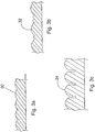
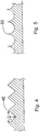
- the Figs. 3 , 4, and 5 demonstrate several different representative unclaimed examples for texturing.
- the first unclaimed examples ( Figs. 3a, 3b, and 3c ) show surfaces 30, 32, 34 which are scalloped.
- the scallops presented are convex in shape toward the reactor chamber. Alternating the scallops can be concave toward the reactor chamber much as presented in Fig. 5 .
- Such surface can be provided on the electrodes, shields for the electrode, and also on the various surfaces found inside of a reactor chamber.
- the unclaimed examples shown in Figs. 4 and 5 include texturing which have a series of peaks 40, 50.
- the effect of this texturing in some instances can be measured by the aspect ratio of the width between peaks to the depth of the valley between the peaks.
- the aspect ratio would be: W D
- a textured surface also increases the surface area upon which materials can be deposited and collected.
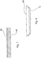
- FIG. 7 Another unclaimed example as shown in Fig. 7 for use especially with such non-volatile films includes the pre-coating of the various surfaces 55 of the reaction chamber in order to promote chemical adhesion.
- Such pre-coating 60 can be done with Titanium (Ti) or Titanium Nitride (TiN).
- Ti Titanium
- TiN Titanium Nitride
- the surface found in the reactor chamber can be pre-coated with materials which are the same as or compatible with the non-volatile films which are being etched.
- Such materials can also include Platinum (Pt), Iridium (Ir), Iridium Oxide (IrO 2 ), Barium Strontium Titanate (BST), Strontium Bismuth Tantalate (SBT), Strontium Titanate (STO), Ruthenium (Ru), Ruthenium Oxide (RuO 2 ), and Lead Zirconium Titanate (PZT).
- Platinum Pt
- Iridium Ir
- Iridium Oxide IrO 2
- BST Barium Strontium Titanate
- SBT Strontium Bismuth Tantalate
- STO Strontium Titanate
- Ru Ruthenium
- RuO 2 Ruthenium Oxide
- PZT Lead Zirconium Titanate
- the sidewalls of the reactor and in particular the sidewalls of the reactor liners can be provided with a matt finish which also promotes good chemical adhesion.
- a matt finish is defined as follows: General texturing of a surface to facilitate the adhesion of various materials. The matting is constructed in such a way as to maximize the surface area penetrated while minimizing spaulding of the deposited film.
- coating or pre-conditioning internal surfaces of the reactor chamber can prevent spaulding, flaking, and delaminating of any materials deposited on the surfaces, beneficially effecting the processing of semiconducting wafers or other substrates
- Fig. 8 shows a shield 70 which has been located adjacent to an upper electrode 80.
- the shield can either be heated, textured, or pre-coated, or a combination of the above and be within the spirit and scope of the invention. Texturing can include grooves, channels, perforations and/or screened surfaces.
- the present invention advantageously uses heated and/or textured and/or pre-coated surfaces that are internal to a reactor chamber in order to ensure that materials deposited thereon adhere and do not flake, spauld or become delaminated, contaminating the process.
Landscapes
- Engineering & Computer Science (AREA)
- Chemical & Material Sciences (AREA)
- Physics & Mathematics (AREA)
- Plasma & Fusion (AREA)
- Analytical Chemistry (AREA)
- Computer Hardware Design (AREA)
- Microelectronics & Electronic Packaging (AREA)
- Power Engineering (AREA)
- General Physics & Mathematics (AREA)
- Manufacturing & Machinery (AREA)
- Condensed Matter Physics & Semiconductors (AREA)
- Materials Engineering (AREA)
- Mechanical Engineering (AREA)
- Metallurgy (AREA)
- Organic Chemistry (AREA)
- Chemical Kinetics & Catalysis (AREA)
- General Chemical & Material Sciences (AREA)
- Drying Of Semiconductors (AREA)
- Chemical Vapour Deposition (AREA)
- Physical Or Chemical Processes And Apparatus (AREA)
Applications Claiming Priority (3)
| Application Number | Priority Date | Filing Date | Title |
|---|---|---|---|
| US453842 | 1995-05-30 | ||
| US45384299A | 1999-12-02 | 1999-12-02 | |
| PCT/US2000/031987 WO2001040540A1 (en) | 1999-12-02 | 2000-11-21 | Improved reactor with heated and textured electrodes and surfaces |
Publications (3)
| Publication Number | Publication Date |
|---|---|
| EP1252359A1 EP1252359A1 (en) | 2002-10-30 |
| EP1252359A4 EP1252359A4 (en) | 2011-01-26 |
| EP1252359B1 true EP1252359B1 (en) | 2020-03-11 |
Family
ID=23802291
Family Applications (1)
| Application Number | Title | Priority Date | Filing Date |
|---|---|---|---|
| EP00980631.6A Expired - Lifetime EP1252359B1 (en) | 1999-12-02 | 2000-11-21 | Method of operating a platinum etch reactor |
Country Status (5)
| Country | Link |
|---|---|
| US (2) | US7439188B2 (enExample) |
| EP (1) | EP1252359B1 (enExample) |
| JP (1) | JP5054874B2 (enExample) |
| AU (1) | AU1786301A (enExample) |
| WO (1) | WO2001040540A1 (enExample) |
Families Citing this family (26)
| Publication number | Priority date | Publication date | Assignee | Title |
|---|---|---|---|---|
| DE60139868D1 (de) * | 2000-06-16 | 2009-10-22 | Ati Properties Inc | Verfahren zum spritzformen, zerstäuben und wärmeaustausch |
| US6496529B1 (en) | 2000-11-15 | 2002-12-17 | Ati Properties, Inc. | Refining and casting apparatus and method |
| US8891583B2 (en) | 2000-11-15 | 2014-11-18 | Ati Properties, Inc. | Refining and casting apparatus and method |
| JP3963431B2 (ja) * | 2002-03-04 | 2007-08-22 | 松下電器産業株式会社 | 半導体装置の製造方法 |
| US6812471B2 (en) | 2002-03-13 | 2004-11-02 | Applied Materials, Inc. | Method of surface texturizing |
| US6933508B2 (en) * | 2002-03-13 | 2005-08-23 | Applied Materials, Inc. | Method of surface texturizing |
| US20040173314A1 (en) * | 2003-03-05 | 2004-09-09 | Ryoji Nishio | Plasma processing apparatus and method |
| TWI342582B (en) * | 2003-07-17 | 2011-05-21 | Applied Materials Inc | Method of surface texturizing |
| JP4594070B2 (ja) * | 2004-04-06 | 2010-12-08 | 三菱電機株式会社 | 半導体レーザ素子及びその製造方法 |
| US7119032B2 (en) * | 2004-08-23 | 2006-10-10 | Air Products And Chemicals, Inc. | Method to protect internal components of semiconductor processing equipment using layered superlattice materials |
| US7578960B2 (en) * | 2005-09-22 | 2009-08-25 | Ati Properties, Inc. | Apparatus and method for clean, rapidly solidified alloys |
| US7803211B2 (en) | 2005-09-22 | 2010-09-28 | Ati Properties, Inc. | Method and apparatus for producing large diameter superalloy ingots |
| US7803212B2 (en) | 2005-09-22 | 2010-09-28 | Ati Properties, Inc. | Apparatus and method for clean, rapidly solidified alloys |
| JP4887910B2 (ja) * | 2006-05-30 | 2012-02-29 | パナソニック株式会社 | プラズマ処理装置 |
| US8748773B2 (en) * | 2007-03-30 | 2014-06-10 | Ati Properties, Inc. | Ion plasma electron emitters for a melting furnace |
| ES2608863T3 (es) | 2007-03-30 | 2017-04-17 | Ati Properties Llc | Horno de fusión que incluye un emisor de electrones de plasma iónico por descarga de hilo |
| JP5474291B2 (ja) | 2007-11-05 | 2014-04-16 | 株式会社アルバック | アッシング装置 |
| US7798199B2 (en) | 2007-12-04 | 2010-09-21 | Ati Properties, Inc. | Casting apparatus and method |
| US8747956B2 (en) | 2011-08-11 | 2014-06-10 | Ati Properties, Inc. | Processes, systems, and apparatus for forming products from atomized metals and alloys |
| DE102015101343A1 (de) * | 2015-01-29 | 2016-08-18 | Aixtron Se | CVD-Reaktor mit dreidimensional strukturierter Prozesskammerdecke |
| US10896950B2 (en) * | 2017-02-27 | 2021-01-19 | Nxp Usa, Inc. | Method and apparatus for a thin film dielectric stack |
| US10923286B2 (en) | 2018-02-21 | 2021-02-16 | Nxp Usa, Inc. | Method and apparatus for compensating for high thermal expansion coefficient mismatch of a stacked device |
| US20190276932A1 (en) * | 2018-03-08 | 2019-09-12 | Shimadzu Corporation | Film forming apparatus and film forming method |
| SG11202108622PA (en) * | 2019-02-06 | 2021-09-29 | Lam Res Corp | Textured silicon semiconductor processing chamber components |
| GB201919220D0 (en) | 2019-12-23 | 2020-02-05 | Spts Technologies Ltd | Method of plasma etching |
| GB201919215D0 (en) | 2019-12-23 | 2020-02-05 | Spts Technologies Ltd | Method and apparatus for plasma etching |
Family Cites Families (68)
| Publication number | Priority date | Publication date | Assignee | Title |
|---|---|---|---|---|
| US3514391A (en) | 1967-05-05 | 1970-05-26 | Nat Res Corp | Sputtering apparatus with finned anode |
| US4033287A (en) | 1976-01-22 | 1977-07-05 | Bell Telephone Laboratories, Incorporated | Radial flow reactor including glow discharge limiting shield |
| US4208241A (en) | 1978-07-31 | 1980-06-17 | Bell Telephone Laboratories, Incorporated | Device fabrication by plasma etching |
| US4680061A (en) | 1979-12-21 | 1987-07-14 | Varian Associates, Inc. | Method of thermal treatment of a wafer in an evacuated environment |
| US4743570A (en) | 1979-12-21 | 1988-05-10 | Varian Associates, Inc. | Method of thermal treatment of a wafer in an evacuated environment |
| US4512391A (en) | 1982-01-29 | 1985-04-23 | Varian Associates, Inc. | Apparatus for thermal treatment of semiconductor wafers by gas conduction incorporating peripheral gas inlet |
| US4508161A (en) | 1982-05-25 | 1985-04-02 | Varian Associates, Inc. | Method for gas-assisted, solid-to-solid thermal transfer with a semiconductor wafer |
| US4457359A (en) | 1982-05-25 | 1984-07-03 | Varian Associates, Inc. | Apparatus for gas-assisted, solid-to-solid thermal transfer with a semiconductor wafer |
| US4542298A (en) | 1983-06-09 | 1985-09-17 | Varian Associates, Inc. | Methods and apparatus for gas-assisted thermal transfer with a semiconductor wafer |
| US4535834A (en) | 1984-05-02 | 1985-08-20 | Varian Associates, Inc. | Method and apparatus for controlling thermal transfer in a cyclic vacuum processing system |
| JPS6372877A (ja) * | 1986-09-12 | 1988-04-02 | Tokuda Seisakusho Ltd | 真空処理装置 |
| US5031571A (en) * | 1988-02-01 | 1991-07-16 | Mitsui Toatsu Chemicals, Inc. | Apparatus for forming a thin film on a substrate |
| JPH02267289A (ja) * | 1989-04-08 | 1990-11-01 | Seiko Epson Corp | ドライ・エッチング法 |
| JPH02298024A (ja) * | 1989-05-12 | 1990-12-10 | Tadahiro Omi | リアクティブイオンエッチング装置 |
| US5556501A (en) * | 1989-10-03 | 1996-09-17 | Applied Materials, Inc. | Silicon scavenger in an inductively coupled RF plasma reactor |
| US5252194A (en) * | 1990-01-26 | 1993-10-12 | Varian Associates, Inc. | Rotating sputtering apparatus for selected erosion |
| JP2755471B2 (ja) * | 1990-06-29 | 1998-05-20 | 日立電線株式会社 | 希土類元素添加光導波路及びその製造方法 |
| US5074456A (en) * | 1990-09-18 | 1991-12-24 | Lam Research Corporation | Composite electrode for plasma processes |
| JPH04316327A (ja) * | 1991-04-15 | 1992-11-06 | Toshiba Corp | ドライエッチング装置及びチャンバの洗浄方法 |
| US5119460A (en) * | 1991-04-25 | 1992-06-02 | At&T Bell Laboratories | Erbium-doped planar optical device |
| US5107538A (en) * | 1991-06-06 | 1992-04-21 | At&T Bell Laboratories | Optical waveguide system comprising a rare-earth Si-based optical device |
| US5277751A (en) | 1992-06-18 | 1994-01-11 | Ogle John S | Method and apparatus for producing low pressure planar plasma using a coil with its axis parallel to the surface of a coupling window |
| JP3214910B2 (ja) * | 1992-08-18 | 2001-10-02 | 富士通株式会社 | 平面導波路型光増幅器の製造方法 |
| US5800618A (en) * | 1992-11-12 | 1998-09-01 | Ngk Insulators, Ltd. | Plasma-generating electrode device, an electrode-embedded article, and a method of manufacturing thereof |
| JP3242166B2 (ja) | 1992-11-19 | 2001-12-25 | 株式会社日立製作所 | エッチング装置 |
| US6001432A (en) * | 1992-11-19 | 1999-12-14 | Semiconductor Energy Laboratory Co., Ltd. | Apparatus for forming films on a substrate |
| JP3381076B2 (ja) | 1992-11-24 | 2003-02-24 | ソニー株式会社 | ドライエッチング方法 |
| JPH06188108A (ja) | 1992-12-21 | 1994-07-08 | Canon Inc | 薄膜抵抗器の製造方法、成膜装置用防着板及び成膜装置 |
| US5303319A (en) * | 1992-12-28 | 1994-04-12 | Honeywell Inc. | Ion-beam deposited multilayer waveguides and resonators |
| US5718813A (en) * | 1992-12-30 | 1998-02-17 | Advanced Energy Industries, Inc. | Enhanced reactive DC sputtering system |
| US5427669A (en) * | 1992-12-30 | 1995-06-27 | Advanced Energy Industries, Inc. | Thin film DC plasma processing system |
| US5613995A (en) * | 1993-04-23 | 1997-03-25 | Lucent Technologies Inc. | Method for making planar optical waveguides |
| JPH0718423A (ja) | 1993-07-06 | 1995-01-20 | Japan Energy Corp | 薄膜形成装置 |
| JP2972506B2 (ja) | 1993-11-02 | 1999-11-08 | 日本電気株式会社 | Ptを主成分とする合金のエッチング方法 |
| US5433835B1 (en) * | 1993-11-24 | 1997-05-20 | Applied Materials Inc | Sputtering device and target with cover to hold cooling fluid |
| US5487822A (en) * | 1993-11-24 | 1996-01-30 | Applied Materials, Inc. | Integrated sputtering target assembly |
| US5475528A (en) * | 1994-03-25 | 1995-12-12 | Corning Incorporated | Optical signal amplifier glasses |
| US5628869A (en) * | 1994-05-09 | 1997-05-13 | Lsi Logic Corporation | Plasma enhanced chemical vapor reactor with shaped electrodes |
| JP3107971B2 (ja) * | 1994-05-17 | 2000-11-13 | 株式会社半導体エネルギー研究所 | 気相反応装置 |
| WO1996000996A1 (en) * | 1994-06-30 | 1996-01-11 | The Whitaker Corporation | Planar hybrid optical amplifier |
| US5483613A (en) * | 1994-08-16 | 1996-01-09 | At&T Corp. | Optical device with substrate and waveguide structure having thermal matching interfaces |
| JPH0874028A (ja) * | 1994-09-01 | 1996-03-19 | Matsushita Electric Ind Co Ltd | 薄膜形成装置および薄膜形成方法 |
| US5555342A (en) * | 1995-01-17 | 1996-09-10 | Lucent Technologies Inc. | Planar waveguide and a process for its fabrication |
| US5772770A (en) * | 1995-01-27 | 1998-06-30 | Kokusai Electric Co, Ltd. | Substrate processing apparatus |
| JPH08259386A (ja) * | 1995-03-20 | 1996-10-08 | Matsushita Electric Ind Co Ltd | 酸化物薄膜の製造方法及びそれに用いる化学蒸着装置 |
| US5874704A (en) | 1995-06-30 | 1999-02-23 | Lam Research Corporation | Low inductance large area coil for an inductively coupled plasma source |
| US5563979A (en) * | 1995-08-31 | 1996-10-08 | Lucent Technologies Inc. | Erbium-doped planar optical device |
| US5719976A (en) * | 1995-10-24 | 1998-02-17 | Lucent Technologies, Inc. | Optimized waveguide structure |
| JP3220631B2 (ja) * | 1995-12-07 | 2001-10-22 | 松下電器産業株式会社 | プラズマ処理方法及び装置 |
| US6214740B1 (en) * | 1996-01-26 | 2001-04-10 | Matsushita Electronics Corporation | Semiconductor manufacturing apparatus |
| US5702770A (en) | 1996-01-30 | 1997-12-30 | Becton, Dickinson And Company | Method for plasma processing |
| US5753566A (en) | 1996-05-23 | 1998-05-19 | Taiwan Semiconductor Manufactured Company, Ltd. | Method of spin-on-glass etchback using hot backside helium |
| US5800619A (en) | 1996-06-10 | 1998-09-01 | Lam Research Corporation | Vacuum plasma processor having coil with minimum magnetic field in its center |
| US5855744A (en) * | 1996-07-19 | 1999-01-05 | Applied Komatsu Technology, Inc. | Non-planar magnet tracking during magnetron sputtering |
| US5708557A (en) | 1996-08-22 | 1998-01-13 | Packard Hughes Interconnect Company | Puncture-resistant electrostatic chuck with flat surface and method of making the same |
| US5661093A (en) | 1996-09-12 | 1997-08-26 | Applied Materials, Inc. | Method for the stabilization of halogen-doped films through the use of multiple sealing layers |
| US6007673A (en) * | 1996-10-02 | 1999-12-28 | Matsushita Electronics Corporation | Apparatus and method of producing an electronic device |
| US5904487A (en) * | 1996-10-08 | 1999-05-18 | Advanced Micro Devices, Inc. | Electrode reshaping in a semiconductor etching device |
| US5841931A (en) * | 1996-11-26 | 1998-11-24 | Massachusetts Institute Of Technology | Methods of forming polycrystalline semiconductor waveguides for optoelectronic integrated circuits, and devices formed thereby |
| US5814154A (en) | 1997-01-23 | 1998-09-29 | Gasonics International | Short-coupled-path extender for plasma source |
| US5847865A (en) * | 1997-02-18 | 1998-12-08 | Regents Of The University Of Minnesota | Waveguide optical amplifier |
| JP2943101B2 (ja) * | 1997-05-07 | 1999-08-30 | 株式会社ミヤコシ | ターンバー装置 |
| US5831262A (en) * | 1997-06-27 | 1998-11-03 | Lucent Technologies Inc. | Article comprising an optical fiber attached to a micromechanical device |
| US6046116A (en) * | 1997-11-19 | 2000-04-04 | Tegal Corporation | Method for minimizing the critical dimension growth of a feature on a semiconductor wafer |
| US6041734A (en) * | 1997-12-01 | 2000-03-28 | Applied Materials, Inc. | Use of an asymmetric waveform to control ion bombardment during substrate processing |
| US6071573A (en) * | 1997-12-30 | 2000-06-06 | Lam Research Corporation | Process for precoating plasma CVD reactors |
| US6157765A (en) * | 1998-11-03 | 2000-12-05 | Lucent Technologies | Planar waveguide optical amplifier |
| US6143078A (en) * | 1998-11-13 | 2000-11-07 | Applied Materials, Inc. | Gas distribution system for a CVD processing chamber |
-
2000
- 2000-11-21 EP EP00980631.6A patent/EP1252359B1/en not_active Expired - Lifetime
- 2000-11-21 WO PCT/US2000/031987 patent/WO2001040540A1/en not_active Ceased
- 2000-11-21 JP JP2001542603A patent/JP5054874B2/ja not_active Expired - Fee Related
- 2000-11-21 AU AU17863/01A patent/AU1786301A/en not_active Abandoned
-
2001
- 2001-06-22 US US09/888,365 patent/US7439188B2/en not_active Expired - Fee Related
-
2008
- 2008-09-02 US US12/203,022 patent/US20080318432A1/en not_active Abandoned
Non-Patent Citations (1)
| Title |
|---|
| None * |
Also Published As
| Publication number | Publication date |
|---|---|
| US20020036064A1 (en) | 2002-03-28 |
| EP1252359A1 (en) | 2002-10-30 |
| JP5054874B2 (ja) | 2012-10-24 |
| US7439188B2 (en) | 2008-10-21 |
| JP2003515960A (ja) | 2003-05-07 |
| AU1786301A (en) | 2001-06-12 |
| US20080318432A1 (en) | 2008-12-25 |
| EP1252359A4 (en) | 2011-01-26 |
| WO2001040540A1 (en) | 2001-06-07 |
Similar Documents
| Publication | Publication Date | Title |
|---|---|---|
| EP1252359B1 (en) | Method of operating a platinum etch reactor | |
| US12266540B2 (en) | Method for fabricating layer structure having target topological profile | |
| KR100892789B1 (ko) | 성막 처리 방법 | |
| US5589003A (en) | Shielded substrate support for processing chamber | |
| KR102788344B1 (ko) | 고성능 코팅을 갖는 반도체 챔버 구성요소들 | |
| JP2018059173A (ja) | 成膜方法 | |
| US8962354B2 (en) | Methods for forming templated materials | |
| CN110402482A (zh) | 半导体装置的制造方法、清洁方法、基板处理装置和程序 | |
| KR101234492B1 (ko) | 기판 처리 방법 | |
| JP2001308077A (ja) | 半導体製造装置 | |
| Menk et al. | Dry etching issues in the integration of ferroelectric thin film capacitors | |
| US20230138555A1 (en) | Plasma processing chamber with multilayer protective surface | |
| US7141512B2 (en) | Method of cleaning semiconductor device fabrication apparatus | |
| TWI877526B (zh) | 具多層塗層之半導體腔室組件 | |
| CN103789747B (zh) | 一种气体喷淋头及制作该气体喷淋头的方法 | |
| KR102539807B1 (ko) | 실리콘 부품을 컨디셔닝하기 위한 방법 | |
| CA2262749C (en) | Production of corrosion-resistant ceramic members | |
| KR20210009154A (ko) | 배치식 기판처리장치 및 그 운용방법 | |
| US6186154B1 (en) | Find end point of CLF3 clean by pressure change | |
| JPH07201742A (ja) | プラズマcvd装置 | |
| KR20220067696A (ko) | 가스 공급부재 및 이를 구비한 기판처리장치 | |
| KR20230054273A (ko) | 파티클 억제 방법 | |
| CN114335338A (zh) | 半导体结构的制造方法、半导体结构及存储器 | |
| CN116230691A (zh) | 半导体检测结构、形成方法以及检测方法 | |
| JPWO2009001744A1 (ja) | エッチング方法およびエッチング装置 |
Legal Events
| Date | Code | Title | Description |
|---|---|---|---|
| PUAI | Public reference made under article 153(3) epc to a published international application that has entered the european phase |
Free format text: ORIGINAL CODE: 0009012 |
|
| 17P | Request for examination filed |
Effective date: 20020621 |
|
| AK | Designated contracting states |
Kind code of ref document: A1 Designated state(s): AT BE CH CY DE DK ES FI FR GB GR IE IT LI LU MC NL PT SE TR |
|
| AX | Request for extension of the european patent |
Free format text: AL;LT;LV;MK;RO;SI |
|
| A4 | Supplementary search report drawn up and despatched |
Effective date: 20101229 |
|
| RAP1 | Party data changed (applicant data changed or rights of an application transferred) |
Owner name: OEM GROUP, INC |
|
| 17Q | First examination report despatched |
Effective date: 20120124 |
|
| STAA | Information on the status of an ep patent application or granted ep patent |
Free format text: STATUS: EXAMINATION IS IN PROGRESS |
|
| REG | Reference to a national code |
Ref country code: DE Ref legal event code: R079 Ref document number: 60049965 Country of ref document: DE Free format text: PREVIOUS MAIN CLASS: C23C0016000000 Ipc: C23C0016440000 |
|
| RIC1 | Information provided on ipc code assigned before grant |
Ipc: C23C 16/44 20060101AFI20190919BHEP Ipc: H01J 37/32 20060101ALI20190919BHEP Ipc: H01L 21/67 20060101ALI20190919BHEP |
|
| GRAP | Despatch of communication of intention to grant a patent |
Free format text: ORIGINAL CODE: EPIDOSNIGR1 |
|
| STAA | Information on the status of an ep patent application or granted ep patent |
Free format text: STATUS: GRANT OF PATENT IS INTENDED |
|
| INTG | Intention to grant announced |
Effective date: 20191114 |
|
| GRAS | Grant fee paid |
Free format text: ORIGINAL CODE: EPIDOSNIGR3 |
|
| GRAA | (expected) grant |
Free format text: ORIGINAL CODE: 0009210 |
|
| STAA | Information on the status of an ep patent application or granted ep patent |
Free format text: STATUS: THE PATENT HAS BEEN GRANTED |
|
| AK | Designated contracting states |
Kind code of ref document: B1 Designated state(s): AT BE CH CY DE DK ES FI FR GB GR IE IT LI LU MC NL PT SE TR |
|
| REG | Reference to a national code |
Ref country code: GB Ref legal event code: FG4D |
|
| REG | Reference to a national code |
Ref country code: CH Ref legal event code: EP |
|
| REG | Reference to a national code |
Ref country code: AT Ref legal event code: REF Ref document number: 1243231 Country of ref document: AT Kind code of ref document: T Effective date: 20200315 |
|
| REG | Reference to a national code |
Ref country code: IE Ref legal event code: FG4D |
|
| REG | Reference to a national code |
Ref country code: DE Ref legal event code: R096 Ref document number: 60049965 Country of ref document: DE |
|
| PG25 | Lapsed in a contracting state [announced via postgrant information from national office to epo] |
Ref country code: FI Free format text: LAPSE BECAUSE OF FAILURE TO SUBMIT A TRANSLATION OF THE DESCRIPTION OR TO PAY THE FEE WITHIN THE PRESCRIBED TIME-LIMIT Effective date: 20200311 |
|
| REG | Reference to a national code |
Ref country code: NL Ref legal event code: MP Effective date: 20200311 |
|
| PG25 | Lapsed in a contracting state [announced via postgrant information from national office to epo] |
Ref country code: GR Free format text: LAPSE BECAUSE OF FAILURE TO SUBMIT A TRANSLATION OF THE DESCRIPTION OR TO PAY THE FEE WITHIN THE PRESCRIBED TIME-LIMIT Effective date: 20200612 Ref country code: SE Free format text: LAPSE BECAUSE OF FAILURE TO SUBMIT A TRANSLATION OF THE DESCRIPTION OR TO PAY THE FEE WITHIN THE PRESCRIBED TIME-LIMIT Effective date: 20200311 |
|
| PG25 | Lapsed in a contracting state [announced via postgrant information from national office to epo] |
Ref country code: NL Free format text: LAPSE BECAUSE OF FAILURE TO SUBMIT A TRANSLATION OF THE DESCRIPTION OR TO PAY THE FEE WITHIN THE PRESCRIBED TIME-LIMIT Effective date: 20200311 |
|
| PG25 | Lapsed in a contracting state [announced via postgrant information from national office to epo] |
Ref country code: PT Free format text: LAPSE BECAUSE OF FAILURE TO SUBMIT A TRANSLATION OF THE DESCRIPTION OR TO PAY THE FEE WITHIN THE PRESCRIBED TIME-LIMIT Effective date: 20200805 |
|
| REG | Reference to a national code |
Ref country code: AT Ref legal event code: MK05 Ref document number: 1243231 Country of ref document: AT Kind code of ref document: T Effective date: 20200311 |
|
| REG | Reference to a national code |
Ref country code: DE Ref legal event code: R071 Ref document number: 60049965 Country of ref document: DE |
|
| REG | Reference to a national code |
Ref country code: CH Ref legal event code: PL |
|
| REG | Reference to a national code |
Ref country code: DE Ref legal event code: R097 Ref document number: 60049965 Country of ref document: DE |
|
| REG | Reference to a national code |
Ref country code: IE Ref legal event code: MK9A |
|
| PLBE | No opposition filed within time limit |
Free format text: ORIGINAL CODE: 0009261 |
|
| REG | Reference to a national code |
Ref country code: BE Ref legal event code: MK Effective date: 20201121 |
|
| STAA | Information on the status of an ep patent application or granted ep patent |
Free format text: STATUS: NO OPPOSITION FILED WITHIN TIME LIMIT |
|
| PG25 | Lapsed in a contracting state [announced via postgrant information from national office to epo] |
Ref country code: ES Free format text: LAPSE BECAUSE OF FAILURE TO SUBMIT A TRANSLATION OF THE DESCRIPTION OR TO PAY THE FEE WITHIN THE PRESCRIBED TIME-LIMIT Effective date: 20200311 Ref country code: AT Free format text: LAPSE BECAUSE OF FAILURE TO SUBMIT A TRANSLATION OF THE DESCRIPTION OR TO PAY THE FEE WITHIN THE PRESCRIBED TIME-LIMIT Effective date: 20200311 Ref country code: IE Free format text: LAPSE BECAUSE OF EXPIRATION OF PROTECTION Effective date: 20201121 Ref country code: DK Free format text: LAPSE BECAUSE OF FAILURE TO SUBMIT A TRANSLATION OF THE DESCRIPTION OR TO PAY THE FEE WITHIN THE PRESCRIBED TIME-LIMIT Effective date: 20200311 |
|
| 26N | No opposition filed |
Effective date: 20201214 |
|
| REG | Reference to a national code |
Ref country code: GB Ref legal event code: PE20 Expiry date: 20201121 |
|
| PG25 | Lapsed in a contracting state [announced via postgrant information from national office to epo] |
Ref country code: IT Free format text: LAPSE BECAUSE OF FAILURE TO SUBMIT A TRANSLATION OF THE DESCRIPTION OR TO PAY THE FEE WITHIN THE PRESCRIBED TIME-LIMIT Effective date: 20200311 Ref country code: GB Free format text: LAPSE BECAUSE OF EXPIRATION OF PROTECTION Effective date: 20201121 |