EP1250741B1 - Inrush current limiting circuit, power source device and power conversion device - Google Patents
Inrush current limiting circuit, power source device and power conversion device Download PDFInfo
- Publication number
- EP1250741B1 EP1250741B1 EP00978044A EP00978044A EP1250741B1 EP 1250741 B1 EP1250741 B1 EP 1250741B1 EP 00978044 A EP00978044 A EP 00978044A EP 00978044 A EP00978044 A EP 00978044A EP 1250741 B1 EP1250741 B1 EP 1250741B1
- Authority
- EP
- European Patent Office
- Prior art keywords
- switching element
- capacitor
- inrush current
- main electrode
- current limiting
- Prior art date
- Legal status (The legal status is an assumption and is not a legal conclusion. Google has not performed a legal analysis and makes no representation as to the accuracy of the status listed.)
- Expired - Lifetime
Links
Images


Classifications
-
- H—ELECTRICITY
- H02—GENERATION; CONVERSION OR DISTRIBUTION OF ELECTRIC POWER
- H02M—APPARATUS FOR CONVERSION BETWEEN AC AND AC, BETWEEN AC AND DC, OR BETWEEN DC AND DC, AND FOR USE WITH MAINS OR SIMILAR POWER SUPPLY SYSTEMS; CONVERSION OF DC OR AC INPUT POWER INTO SURGE OUTPUT POWER; CONTROL OR REGULATION THEREOF
- H02M1/00—Details of apparatus for conversion
- H02M1/36—Means for starting or stopping converters
-
- H—ELECTRICITY
- H02—GENERATION; CONVERSION OR DISTRIBUTION OF ELECTRIC POWER
- H02H—EMERGENCY PROTECTIVE CIRCUIT ARRANGEMENTS
- H02H9/00—Emergency protective circuit arrangements for limiting excess current or voltage without disconnection
- H02H9/001—Emergency protective circuit arrangements for limiting excess current or voltage without disconnection limiting speed of change of electric quantities, e.g. soft switching on or off
-
- H—ELECTRICITY
- H03—ELECTRONIC CIRCUITRY
- H03K—PULSE TECHNIQUE
- H03K17/00—Electronic switching or gating, i.e. not by contact-making and –breaking
- H03K17/16—Modifications for eliminating interference voltages or currents
- H03K17/161—Modifications for eliminating interference voltages or currents in field-effect transistor switches
- H03K17/162—Modifications for eliminating interference voltages or currents in field-effect transistor switches without feedback from the output circuit to the control circuit
- H03K17/163—Soft switching
-
- H—ELECTRICITY
- H03—ELECTRONIC CIRCUITRY
- H03K—PULSE TECHNIQUE
- H03K17/00—Electronic switching or gating, i.e. not by contact-making and –breaking
- H03K17/16—Modifications for eliminating interference voltages or currents
- H03K17/168—Modifications for eliminating interference voltages or currents in composite switches
-
- H—ELECTRICITY
- H02—GENERATION; CONVERSION OR DISTRIBUTION OF ELECTRIC POWER
- H02H—EMERGENCY PROTECTIVE CIRCUIT ARRANGEMENTS
- H02H7/00—Emergency protective circuit arrangements specially adapted for specific types of electric machines or apparatus or for sectionalised protection of cable or line systems, and effecting automatic switching in the event of an undesired change from normal working conditions
- H02H7/10—Emergency protective circuit arrangements specially adapted for specific types of electric machines or apparatus or for sectionalised protection of cable or line systems, and effecting automatic switching in the event of an undesired change from normal working conditions for converters; for rectifiers
- H02H7/12—Emergency protective circuit arrangements specially adapted for specific types of electric machines or apparatus or for sectionalised protection of cable or line systems, and effecting automatic switching in the event of an undesired change from normal working conditions for converters; for rectifiers for static converters or rectifiers
- H02H7/122—Emergency protective circuit arrangements specially adapted for specific types of electric machines or apparatus or for sectionalised protection of cable or line systems, and effecting automatic switching in the event of an undesired change from normal working conditions for converters; for rectifiers for static converters or rectifiers for inverters, i.e. DC/AC converters
- H02H7/1222—Emergency protective circuit arrangements specially adapted for specific types of electric machines or apparatus or for sectionalised protection of cable or line systems, and effecting automatic switching in the event of an undesired change from normal working conditions for converters; for rectifiers for static converters or rectifiers for inverters, i.e. DC/AC converters responsive to abnormalities in the input circuit, e.g. transients in the DC input
-
- Y—GENERAL TAGGING OF NEW TECHNOLOGICAL DEVELOPMENTS; GENERAL TAGGING OF CROSS-SECTIONAL TECHNOLOGIES SPANNING OVER SEVERAL SECTIONS OF THE IPC; TECHNICAL SUBJECTS COVERED BY FORMER USPC CROSS-REFERENCE ART COLLECTIONS [XRACs] AND DIGESTS
- Y10—TECHNICAL SUBJECTS COVERED BY FORMER USPC
- Y10S—TECHNICAL SUBJECTS COVERED BY FORMER USPC CROSS-REFERENCE ART COLLECTIONS [XRACs] AND DIGESTS
- Y10S323/00—Electricity: power supply or regulation systems
- Y10S323/908—Inrush current limiters
Definitions
- the present invention relates to an inrush current limiting circuit, a power source device and a power conversion device; in particular, relates to an improvement thereof to limit an inrush current with high reliability and durability while reducing the overall weight and volume of the device even under a high rated power.
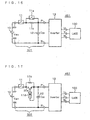
- Fig. 16 is a circuit diagram showing a structure of a conventional power conversion device (which will be hereinafter referred to as "first prior art") having an inrush current limiting circuit.
- This power conversion device 451 comprises a main power source 10, an inrush current limiting circuit 301 and an inverter 13.
- the main power source 10 is connected to input terminals PP and NN of the inrush current limiting circuit 301, and the inverter 13 is connected to the output terminals P and N.
- the power conversion device 451 is utilized by connecting a three-phase load 100, such as a motor, to output terminals U, V and W of the inverter 13.
- the inrush current limiting circuit 301 comprises switches 11 and 11a, a resistor 11b, and a capacitor 12.
- the main power source 10 supplies the input terminals PP and NN with a DC (i.e. direct current) source voltage V DCI .
- the capacitor 12 so functions as to hold the source voltage V DCI at a constant level by means of its capacitance C DC .
- the switch 11, structured as a relay, functions as a main switch that turns ON when starting the inverter 13 and turns OFF when stopping it.
- the switch 11a and the resistor 11b are interposed between the main power source 10 and the capacitor 12 so as to limit an inrush current which flows to charge the capacitor 12 immediately after the switch 11 turns on. After the switch 1 turns ON to start the inverter 13, the switch 11a remains OFF until charging of the capacitor 12 is almost completed. Accordingly, the inrush current is limited by the resistor 11b.
- the switch 11 and the switch 11a have to operate mechanically while a high voltage being applied, the reliability and durability thereof have been problematic. In particular, arcing is influential to the reliability and durability. Moreover, conduction losses of both the switch 11 and the switch 11a during the normal operation of the inverter 13 have also been not negligible concerns.
- Fig. 17 is a circuit diagram showing a structure of another conventional power conversion device (which will be hereinafter referred to as "second prior art") having an inrush current limiting circuit.
- This power conversion device 452 is disclosed in Japanese Patent Application Laid-Open No. 8-289546 (1996) , and is characteristically different from the power conversion devices 451 in that a transistor 30a and a base drive circuit 11d are used for an inrush current limiting circuit 302 in place of the switch 11a.
- the power conversion device 452 eliminates the problem arising from the switch 11a, it still needs the resistor 11b which must have a high rated power. Therefore, the power conversion device 452 has also been disadvantageous in that the weight and volume of the device are large and the manufacturing cost thereof is high. Further, the switch 11 has to operate mechanically while a high voltage being applied similarly to that of the power conversion device 451, and therefore, the reliability and durability of the switch 11 has been problematic.
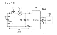
- Fig. 18 is a circuit diagram showing a structure of still another conventional power conversion device (which will be hereinafter referred to as "third prior art") having an inrush current limiting circuit.
- This power conversion device 453 is characteristically different from the power conversion device 451 according to the first prior art in that an NTC (negative coefficient thermistor) 11c is used for an inrush current limiting circuit 303 in place of the switch 11a and the resistor 11b.
- NTC negative coefficient thermistor
- the NTC 11c is low in temperature, it has high resistance.
- the temperature of the NTC 11c rapidly rises up due to loss heat generated in the NTC 11c. Accordingly, the resistance of the NTC 11c rapidly decreases, which decreases loss in the NTC 11c.
- an object of the present invention to obtain an inrush current limiting circuit which eliminates the above mentioned problems and limits an inrush current with high reliability and durability while reducing overall weight and volume of the device even under a high rated power, and to provide a power source device and a power conversion device having the inrush current limiting circuit.
- a first aspect of the present invention is directed to an inrush current limiting circuit as disclosed in claim 1.
- the inrush current limiting circuit further comprises: a first resistor interposed between the one main electrode and the control electrode of the first switching element and connected in series to the second capacitor.
- the inrush current limiting circuit further comprises: a first diode connected in inverse-parallel to the first switching element.
- the inrush current limiting circuit further comprises: a drive circuit connected to the control electrode of the first switching element, and driving the first switching elements in response to a control signal.
- the drive circuit comprises a first output resistor interposed into a path of a drive current which drives the first switching element to turn ON.
- the drive circuit comprises: a second switching element, one main electrode thereof being connected to a source line; a first output resistor, one end thereof being connected to other main electrode of the second switching element, and other end thereof being connected to the control electrode of the first switching element; and a third switching element, one main electrode thereof being connected to the control electrode of the first switching element, other main electrode thereof being connected to other main electrode of said first switching element, and a control electrode thereof being connected to a control electrode of the second switching element.
- the inrush current limiting circuit further comprises: a switch connected in series to the first capacitor and the first switching element.
- An eighth aspect of the present invention is directed to a power source device.
- the power source device comprises: an inrush current limiting circuit according to the first aspect, a DC power source, one end thereof being connected to other end of the first capacitor, and other end thereof being connected to other main electrode of the first switching element; and a switch interposed into a path of a current flowing in circular through the first capacitor, the first switching element and the DC power source.
- a ninth aspect of the present invention is directed to a power conversion device.
- the power conversion device comprises: an inrush current limiting circuit according to the first aspect, a fourth switching element, one main electrode thereof being connected to the one end of the first capacitor; a fifth switching element, one main electrode thereof being connected to other main electrode of the fourth switching element, and other main electrode thereof being connected to the other end of the first capacitor, a sixth switching element, one main electrode thereof being connected to the one end of the first capacitor; and a seventh switching element, one main electrode thereof being connected to other main electrode of the sixth switching element, and other main electrode thereof being connected to the other end of the first capacitor.
- the power conversion device further comprises: a controller unit controlling the fourth to seventh switching elements so as to perform a normal operation of the fourth to seventh switching elements.
- the device is used by connecting a DC power source to the other end of the first capacitor and the other end of the first switching element and connecting any one of various toads supplied with a power to the one end and the other end of the first capacitor.
- a fluctuation in a source voltage supplied to the load is suppressed by the first capacitor, and an inrush current flowing through the first capacitor is limited by the first switching element and the second capacitor.
- the first switching element gradually turns ON due to the second capacitor to thereby limit the inrush current
- the power resistor through which a large current flows is removed contrary to the first and second prior arts, and it is possible to set a rated power high contrary to the third prior art. Accordingly, the overall weight and volume of the device can be reduced even under a high rated power.
- the power resistor is removed, when an external switch is turned ON to supply a source voltage, a high voltage is not applied to the switch. Therefore, the reliability and durability of the switch are not harmed.
- the first resistor is interposed between the first capacitor and the control electrode of the first switching element in addition to the second capacitor, the first switching element is prevented from oscillating and from prematurely turning ON immediately after the external switch turning ON to supply the source voltage. Further, an initial charging current, which flows through the first and second capacitors immediately after the external switch turning ON, is effectively limited by the first resistor.
- the first diode since the first diode is connected in inverse-parallel to the first switching element, the first switching element is protected from a reverse current.
- a small signal transmitted as a control signal can easily drive the first switching element having a high rated power.
- the first switching element since the drive current driving the first switching element to turn ON is limited by the first output resistor, the first switching element turns ON more gradually so as to limit the inrush current more effectively.
- the first switching element since the first output resistor is provided, the first switching element turns ON more gradually so as to limit the inrush current more effectively. Further, since the second switching element and the third switching element are connected in series and only one of them turns ON, a leak current can be suppressed, thereby reducing drive power consumption.
- the switch since the switch is provided, the supply of the source voltage can be started and stopped without preparing an external switch. Further, since the power resistor through which a large current flows is removed contrary to the first and second prior arts, a high voltage is not applied to the switch when the switch turns ON. Therefore, the reliability and durability of the switch are improved.
- the device according to the first aspect of the present invention is provided as an inrush current limiting circuit, such a power source device is implemented as to limit the inrush current with high reliability and durability, reducing the overall weight and volume of the device and coping with a high rated power.
- the device according to the first aspect of the present invention is provided as an inrush current limiting circuit, such a power conversion device is implemented as to limit the inrush current with high reliability and durability, reducing the overall weight and volume of the device and coping with a high rated power.
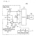
- Fig. 1 is a circuit diagram showing a structure of a power conversion device according to the first preferred embodiment of the present invention.
- the same reference characters are allotted to the same parts or the corresponding parts (i.e. parts having the same functions) as those in the conventional devices shown in Figs. 16 to 18 so as to make clear the relationship therebetween.
- the power conversion device 401 shown in Fig. 1 comprises a main power source 10, an inrush current limiting circuit 1 and an inverter 13.
- the main power source 10 is connected to input terminals PP and NN of the inrush current limiting circuit 1, and the inverter 13 is connected to output terminals P and N.
- the power conversion device 401 is utilized by connecting a three-phase load 100, such as a motor, to output terminals U, V and W of the inverter 13.
- the inrush current limiting circuit 1 comprises a switch 11, a capacitor 12, a switching element 30, a diode 31, a capacitor 32, a resistor 33, a drive circuit 20 and an initial charge controller unit 2.
- the main power source 10 supplies the input terminals PP and NN with a DC source voltage V DCI .
- the capacitor 12 so functions as to hold the source voltage V DCI at a constant level by means of its capacitance C DC .
- the switch 11, structured as a relay, functions as a main switch that turns ON when starting the inverter 13 and turns OFF when stopping it.
- the switching element 30 is of a charge driven type, and will be supposed to be an IGBT as an example in the following description except for in the fifth preferred embodiment.
- a pair of main electrodes of the switching element 30 are a collector and an emitter, and a control electrode thereof is a gate.
- the collector of the switching element 30 is connected to one end of the capacitor 12, and the emitter is connected to the input terminal NN.
- the switch 11, the capacitor 12 and the switching element 30 are connected in series to one another.
- a serial circuit formed thereof is connected to the input terminals PP and NN at its one and the other ends, respectively.
- an order of the capacitor 12 and the switching element 30 placed in the serial circuit is unlimited.
- the output terminals P and N are .connected to one and the other ends of the capacitor 12, respectively.
- the capacitor 32 having a capacitance C 1 and the resistor 33 having a resistance R 1 are connected in series to each other.
- a serial circuit formed of the capacitor 32 and the resistor 33 is connected to the collector and the gate of the switching element 30 at its one and the other ends, respectively.
- the switching element 30, thereby, so functions to limit an inrush current flowing through the capacitor 12 immediately after the switch 11 turns ON. The operation of the switching element 30 will be described in detail later.
- the diode 31 is connected in parallel to the switching element 30 in such a direction that a forward current flows through the diode 31 and the switching element 30 in circular. In the present specification, it is referred to as "connected in inverse-parallel" that a diode is connected to a switching element in such a direction that the forward current flows in circular. The diode 31 protects the switching element 30 from the reverse current.
- the drive circuit 20 which is connected to the gate of the switching element 30, transmits a gate voltage V G to the gate in response to a control signal V IN to thereby drive the switching element 30.
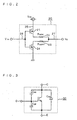
- the drive circuit 20 is configured as shown in a circuit diagram of Fig. 2 , for example.
- the drive circuit 20 shown in Fig. 2 comprises switching elements 21 and 24, and output resistors 22 and 23.
- Each of the switching elements 21 and 24 is formed as a MOSFET (though bipolar transistors can equally be used), a pair of main electrodes thereof are a drain and a source, and a control electrode thereof is a gate.
- the switching element 21, which is a P-type MOSFET is connected to a higher potential source line 25 at its source.
- the resistor 22 is connected to the drain of the switching element 21 at its one end and to the gate of the switching element 30 at its other end through a signal line 27.
- the switching element 24, which is an N-type MOSFET is connected to the input terminal NN at its source through a lower potential source line and to the gate of the switching element 21 at its gate.
- the control signal V IN is input to the gates of the two switching elements 21 and 24 through a signal line 26.
- the resistor 23 is connected to the drain of the switching element 24 at its one end and to the gate of the switching element 30 at its other end through the signal line 27.
- the two switching elements 21 and 24 exclusively turn ON on the basis of the control signal V IN .
- the switching element 21 turns ON to thereby output a drive current that ON-drives the switching element 30 (i.e. drives the switching element 30 to turn ON).
- a resistance R GON of the output resistor 22 functions as an output resistance while the switching element 30 being ON-driven.
- the switching element 24 turns ON to thereby sink a drive current that OFF-drives the switching element 30 (i.e. drives the switching element 30 to turn OFF).
- a resistance R GOFF of the output resistor 23 functions as an output resistance while the switching element 30 being OFF-driven.
- the resistance R GOFF is set at a few ⁇ or less in order to speed up the turn-OFF of the switching element 30 and to prevent any possible faulty turn-ON of the switching element 30.
- the resistance R CON is set at higher values in order to slow down the turn-ON of the switching element 30 and thereby limit the inrush current flowing through the capacitor 12.
- the initial charge controller unit 2 transmits a control signal Rel 1 to the switch 11 and transmits the control signal V IN to the drive circuit 20 to thereby control the switch 11 and the switching element 30.
- the initial charge controller unit 2 controls the switch 11 and the switching element 30 to turn ON on receiving a start instruction from outside.
- the initial charge controller unit 2 also controls the switch 11 and the switching element 30 to turn OFF on receiving a stop instruction from outside.
- the start and stop instructions are input by an operator operating a switch, which is not shown, for example.
- a combination of the main power source 10 and the inrush current limiting circuit 1 forms a power source device having an inrush current limiting function.
- the switching element 30 is of a charge driven type, i.e. a voltage controlled type.
- the switching element 30, therefore, is controlled by charging (when turning ON) and discharging (when turning OFF) its equivalent input capacitance.
- Fig. 3 is a circuit diagram showing the simplified equivalent circuit of the switching element 30.
- Fig. 3 shows an example of the switching element 30 being an IGBT, the same principle applies also to a MOSFET.
- the switching element 30 equivalently includes, a gate-emitter capacitance C DE , a gate-collector capacitance (also referred to as a reverse transfer capacitance or a Miller capacitance) C DC , and a collector-emitter capacitance C CE .
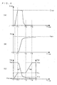
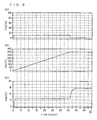
- Fig. 4 is a timing chart showing change in voltages and currents at various portion in the current limiting circuit 1 while the switching element 30 is turning ON without the capacitor 32 and the resistor 33 connected.
- its input capacitance which consists of the gate-emitter capacitance C DE and the gate-collector capacitance C OC must be charged by the drive circuit 20.
- the gate emitter capacitance C GE starts to be charged by the drive current flowing through the resistance R GON .
- the collector current (equal to a charging current I CHG flowing through the capacitor 12) starts to flow through the switching element 30.
- the collector-emitter voltage V CE remains at its high OFF-state value (i.e. the source voltage V DCI of the main power source 10).
- the collector-emitter voltage V CE starts to drop rapidly requiring more charging current to be supplied to the gate-collector capacitance C GC (which is referred to as Miller effect) and that is why the gate-emitter voltage V GE remains almost constant around the voltage Vm (i.e. Miller voltage) during the interval T1-T2.
- the gate-emitter voltage V GE starts to increase again until it reaches its maximum value (i.e. the source voltage V GC of the drive circuit 20) at a time T3, and the collector emitter voltage V CE reaches its lowest ON-state value (i.e. the collector-emitter saturation voltage V CE(sat) .
- the switching element 30 Since the switching element 30 is connected in series between the main power source 10 and the capacitor 12 as Fig. 1 shows, we note that the charged voltage V DC across the capacitor 12 ((B) of Fig. 4 ) will be a reverse image of the collector-emitter voltage V CE ((C) of Fig. 4 ).
- the change rate (i.e. dV DC /dt) of the charged voltage V DC across the capacitor 12 is defined by the turn-ON process of the switching element 30 during the period T1-T2.
- the change rate of the charged voltage V DC determines the charging current I CHD (i.e. the inrush current) flowing from the main power source 10 through the capacitor 12 as part (A) of Fig. 4 shows
- we can control the charging current I CHD by controlling the turn-ON process of the switching element 30 during the period T1-T2.
- the inrush-current can be reduced by reducing the change rate of the charged voltage V DC across the capacitor 12 during the period T1-T2, or equivalently, by increasing the length of the period T1-T2.
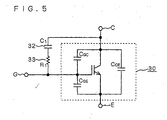
- This can be achieved by adding the capacitor 32 outside the switching element 30 as a circuit diagram of Fig. 5 shows.
- the capacitance C 1 of the capacitor 32 functions as an additional gate-collector capacitance.
- Fig. 6 is a timing chart showing change in voltages and currents at various portion in the current limiting circuit 1 while the switching element 30 is turning ON with the capacitor 32 and the resistor 33 connected as Fig. 5 shows.
- the reduced change rate of the charged voltage V DC during the period T1a-T2a because of the extra time needed to charge the external capacitor 32.
- the resulting decrease in the inrush current i.e. the charging current I CHG ) flowing through the capacitor 12.
- the switch 11 is kept OFF and also the switching element 30 is kept OFF by switching OFF the switching element 21 and switching ON the switching element 24.
- the initial charge controller unit 2 controls the switch 11 to turn ON, an initial charging current will start to flow from the main power supply 10 through the switch 11, the capacitor 12, the capacitor 32, the resistor 33, the resistor 23, and the switching element 24.
- This initial charging current will be limited mainly by the resistor 33 because the resistance R GOFF of the resistor 23 is selected to have a small value (few ⁇ ) or less as mentioned above.
- the initial charge controller unit 2 transmits the control signal V IN to the drive circuit 20 so as to turn ON the switching element 30. As a result, the operation shown in Fig. 6 is performed. After the capacitor 12 is sufficiently charged and thereby the charged voltage V DC reaches the source voltage V DCI , the inverter 13 starts the normal operation. When the inverter 13 is stopped, the initial charge controller unit 2 turns OFF the switch 11 and the switching element 30.
- the drive circuit 20 is configured as Fig. 2 shows.
- the circuit parameters used in the simulation are as follows:
- the inrush current flowing through the capacitor 12 is limited by the switching element 30 and the capacitor 32. Further, since the switching element 30 gradually turns ON due to the capacitor 32 to thereby limit the inrush current, the power resistor 11b through which a large current flows is removed contrary to the first and second prior arts, and it is possible to set a rated power high contrary to the third prior art. Accordingly, the overall weight and volume of the device can be reduced even under a high rated power. Moreover, since the power resistor 11b is removed, a high voltage is not applied to the switch 11 when the switch 11 turns ON. Therefore, the reliability and durability of the switch 11 are improved.
- the resistor 33 is connected in series to the capacitor 12, the switching element 30 is prevented from oscillating at its gate, and from prematurely turning ON immediately after the switch 11 turns ON.
- an initial charging current, which flows through the capacitors 12 and 32 immediately after the switch 11 turns ON, is effectively limited by the resistor 33.
- the switching element 30 since the drive current ON-driving the switching element 30 is limited by the resistance R GON of the output resistor 22, the switching element 30 turns ON more gradually so as to limit the inrush current more effectively. Further, since the switching elements 21 and 24 are connected in series and turn ON exclusively with each other, a leak current can be suppressed, and thereby drive power consumption can be reduced.
- Fig. 9 is a circuit diagram showing a structure of the drive circuit 20 according to the second preferred embodiment of the present invention.
- This drive circuit 20 is characteristically different from the drive circuit 20 according to the first preferred embodiment in that the drain of the switching element 24 and the gate of the switching element 30 are connected to each other through the signal line 27 without a resistor interposed. Since the resistor 23 is removed from the drive circuit 20 according to the first preferred embodiment, the device configuration is advantageously simplified. Further, the current OFF-driving the switching element 30 is not limited by the resistor 23, and therefore, the turn-OFF of the switching element 30 is speeded up.
- Fig. 10 is a circuit diagram showing a structure of the drive circuit 20 according to the third preferred embodiment of the present invention.
- This drive circuit 20 is characteristically different from the drive circuit 20 according to the first preferred embodiment in that the drain of the switching element 21 and the drain of the switching element 24 are connected to each other, and a parallel circuit formed of the resistor 22 and a diode 29 connected in parallel is interposed between a connection of the two switching elements 21, 24 and the gate of the switching element 30.
- the diode 29 is placed in such a direction that its forward current functions as the drive current OFF-driving the switching element 30.
- the drive current ON-driving the switching element 30 is limited by the output resistor 22 without intervention of the diode 29 as well as in the drive circuit 20 shown in Fig. 2 .
- the drive current OFF-driving the switching element 30, flows through the diode 29. Accordingly, the turn-OFF of the switching element 30 is speeded up similarly to that in the drive circuit 20 shown in Fig. 9 .
- Fig. 11 is a circuit diagram showing a structure of the drive circuit 20 according to the fourth preferred embodiment of the present invention.
- This drive circuit 20 is characteristically different from the drive circuit 20 according to the third preferred embodiment in that the switching element 21 is replaced with a resistor 28.
- the drive current ON-driving the switching element 30 is limited by the total resistance of the resistance R GON of the output resistor 22 and the resistance R D of the resistor 28 without the intervention of the diode 29.
- the drive current OFF-driving the switching element 30 flows through the diode 29.
- the turn-OFF of the switching element 30, therefore, is speeded up similarly to that in the drive circuit 20 shown in Fig. 10 .
- the drive circuits 20 shown in Figs. 2 , 9 and 10 have advantage in that the leak current flowing from the higher potential source line 25 to the lower potential source line is suppressed, and thereby drive power consumption can be reduced.
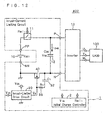
- Fig. 12 is a circuit diagram showing a structure of a power conversion device according to the fifth preferred embodiment of the present invention.
- This power conversion device 402 is characteristically different from the power conversion device 401 according to the first preferred embodiment in that a MOSFET 40 is used for the switching element 30.
- a switching element of a charge driven type can generally be used for the switching element 30.
- the IGBT in the power conversion device 401 and the MOSFET in the power conversion device 402 are widely used, and those having various ratings are advantageously available.
- Fig. 13 is a circuit diagram showing a structure of a power conversion device according to the sixth preferred embodiment of the present invention.
- This power conversion device 403 is characteristically different from the power conversion device 401 according to the first preferred embodiment in that the switching element 30 and the diode 31 are interposed into a higher potential source line connecting the input terminal PP and the output terminal P.
- the switch 11, the switching element 30 and the capacitor 12 are connected in series to one another, and the output terminals PP and NN are connected to one and the other ends of the capacitor 12, respectively.
- Fig. 13 shows other example of the general configuration than that of Fig. 1 .
- Fig. 14 is a circuit diagram showing a structure of a power conversion device according to the seventh preferred embodiment of the present invention.
- This power conversion device 404 is characteristically different from the power conversion device 401 according to the first preferred embodiment in that the inverter 13 comprises an integrated controller unit 201.
- the integrated controller unit 201 functions simultaneously both as a main controller unit that controls a group of the switching elements 51, 54, 61, 64, 71 and 74 provided in the inverter 13 to perform the normal operation and as the initial charge controller unit 2, which controls the switch 11 and the switching element 30 provided in the inrush current limiting circuit 1.
- the integrated controller unit 201 comprises a CPU 203 and a memory 204.
- the CPU 203 operates on the basis of a program stored in the memory 204 to thereby implement the normal operation of the group of the switching elements 51, 54, 61, 64, 71 and 74, and to control the switch 11 and the switching element 30.
- each of the switching elements 51, 54, 61, 64, 71 and 74 is a semiconductor element that controls a main current flowing across the same through a pair of main electrodes in response to a signal input to a control electrode.
- the same is a power switching element e.g. a power IGBT, a power bipolar transistor, and a power MOSFET.
- the power IGBT advantageously has low saturation voltage V CH(GU) which is defined as a voltage between the pair of the main electrodes in a conducting (ON) state, and is of voltage control type, which can easily be controlled. Therefore, each of the switching elements 51; 54, 61, 64, 71 and 74 will be supposed to be a power IGBT in the following description.
- Collectors of the switching elements 51, 61 and 71 are connected to the output terminal P of the inrush current limiting circuit 1.
- Collectors of the switching elements 54, 64 and 74 are connected to emitters of the switching elements 51, 61 and 71, respectively, and emitters are connected to the output terminal N of the inrush current limiting circuit 1.
- the output terminal U of the inverter 13 is connected to a connection between the switching elements 51 and 54.
- the output terminal V is connected to a connection between the switching elements 61 and 64.
- the output terminals W is connected to a connection between the switching elements 71 and 74.
- the inverter 13 further comprises freewheeling diodes 52, 55, 62, 65, 72 and 75, and drive circuits 50, 53, 60, 63, 70 and 73.
- the freewheeling diodes 52, 55, 62, 65, 72 and 75 are respectively connected in inverse-parallel to the switching elements 51, 54, 61, 64, 71 and 74.
- the freewheeling diodes 52, 55, 62, 65, 72 and 75 are provided in order to protect the switching elements 51, 54, 61, 64, 71 and 74 from reverse currents, respectively.
- the drive circuits 50, 53, 60, 63, 70 and 73 are connected to gates of the switching elements 51, 54, 61, 64, 71 and 74, respectively.
- the drive circuits 50, 53, 60, 63, 70 and 73 respectively drive the switching elements 51, 54, 61, 64, 71 and 74 in response to control signals U P , U N , V P , V N , W P and W N , respectively.
- the integrated controller unit 201 can also be divided into the main controller unit that outputs the control signals U P , U N , V P , V N , W P and W N to thereby perform the normal operation of the switching elements 51, 54, 61, 64, 71 and 74-and the initial charge controller unit 2, which controls the switch 11 and the switching element 30.
- the initial charge controller unit 2 can be structured to receive the start and stop instructions from the main controller unit:
- the configuration shown in Fig. 14 where the main controller unit and the initial charge controller unit 2 are integrated into the single integrated controller unit 201 advantageously enables the overall weight and volume and the manufacturing cost of the device to be reduced.
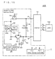
- Fig. 15 is a circuit diagram showing a structure of a power conversion device according to the eighth preferred embodiment of the present invention.
- This power conversion device 405 is characteristically different from the power conversion device 401 according to the first preferred embodiment in that it comprises a rectifier circuit 301 converting an AC voltage input from an external AC power source 300 into the DC source voltage V DCI .
- the rectifier circuit 301 applies the source voltage V DCI between the input terminals PP and NN. Accordingly, the power conversion device 405 can be used only by connecting an available AC power source 300 without preparing an external DC power source.
Landscapes
- Engineering & Computer Science (AREA)
- Power Engineering (AREA)
- Inverter Devices (AREA)
- Dc-Dc Converters (AREA)
- Emergency Protection Circuit Devices (AREA)
Applications Claiming Priority (1)
| Application Number | Priority Date | Filing Date | Title |
|---|---|---|---|
| PCT/JP2000/008492 WO2002045232A1 (en) | 2000-11-30 | 2000-11-30 | Inrush current limiting circuit, power source device and power conversion device |
Publications (2)
| Publication Number | Publication Date |
|---|---|
| EP1250741A1 EP1250741A1 (en) | 2002-10-23 |
| EP1250741B1 true EP1250741B1 (en) | 2008-02-13 |
Family
ID=11736747
Family Applications (1)
| Application Number | Title | Priority Date | Filing Date |
|---|---|---|---|
| EP00978044A Expired - Lifetime EP1250741B1 (en) | 2000-11-30 | 2000-11-30 | Inrush current limiting circuit, power source device and power conversion device |
Country Status (5)
| Country | Link |
|---|---|
| US (1) | US6735098B2 (enExample) |
| EP (1) | EP1250741B1 (enExample) |
| JP (1) | JP4236924B2 (enExample) |
| DE (1) | DE60038050T2 (enExample) |
| WO (1) | WO2002045232A1 (enExample) |
Families Citing this family (28)
| Publication number | Priority date | Publication date | Assignee | Title |
|---|---|---|---|---|
| KR100632980B1 (ko) | 2002-12-20 | 2006-10-11 | 마쯔시다덴기산교 가부시키가이샤 | 게이트 드라이버, 이 게이트 드라이버를 포함하는 모터구동 장치, 및 이 모터 구동 장치를 장착한 기기 |
| GB2401257A (en) * | 2003-04-30 | 2004-11-03 | Bombardier Transp | Transferring electric power to a load |
| US7710748B2 (en) * | 2004-04-13 | 2010-05-04 | Texas Instruments (Cork) Limited | AC/DC converter comprising plural converters in cascade |
| JP4682985B2 (ja) * | 2005-07-06 | 2011-05-11 | パナソニック株式会社 | ブラシレスdcモータおよびそれを搭載した電気機器 |
| TW200713762A (en) * | 2005-09-06 | 2007-04-01 | Acbel Polytech Inc | AC-DC converter capable of actively suppressing inrush current |
| JP4910369B2 (ja) * | 2005-11-15 | 2012-04-04 | トヨタ自動車株式会社 | 電源制御装置 |
| JP4995030B2 (ja) * | 2006-12-22 | 2012-08-08 | プライムアースEvエナジー株式会社 | 開閉制御装置、突入電流制限回路、及び電池付き突入電流制限回路 |
| US8027142B2 (en) * | 2007-10-25 | 2011-09-27 | Honeywell International Inc. | Current-protected driver circuit for ignition exciter unit |
| US8773086B1 (en) * | 2007-12-07 | 2014-07-08 | Marvell International Ltd. | Circuits and methods for dynamic voltage management |
| JP2009183096A (ja) * | 2008-01-31 | 2009-08-13 | Seiko Epson Corp | 電源回路 |
| FR2932031B1 (fr) * | 2008-05-29 | 2012-12-14 | Airbus France | Dispositif de precharge d'un convertisseur a decoupage, ensemble et aeronef le comportant. |
| US7929323B2 (en) * | 2008-09-26 | 2011-04-19 | Rockwell Automation Technologies, Inc. | Method and apparatus for pre-charging power converters and diagnosing pre-charge faults |
| TWI586216B (zh) | 2008-10-08 | 2017-06-01 | Holdip Ltd | 照明系統之改良 |
| GB2470583A (en) * | 2009-05-28 | 2010-12-01 | Technelec Ltd | Half bridge inverter having reduced in-rush current |
| US9005788B2 (en) | 2009-07-06 | 2015-04-14 | Amperex Technology Limited | Management scheme for multiple battery cells |
| CN201656461U (zh) * | 2010-02-26 | 2010-11-24 | 国基电子(上海)有限公司 | 突波电流抑制装置及使用其的电子设备 |
| JP2011188271A (ja) * | 2010-03-09 | 2011-09-22 | Mitsubishi Electric Corp | ゲート駆動回路 |
| US8816625B2 (en) | 2011-10-27 | 2014-08-26 | Rockwell Automation Technologies, Inc. | Integrated regenerative AC drive with solid state precharging |
| US9083274B2 (en) | 2013-04-08 | 2015-07-14 | Rockwell Automation Technologies, Inc. | Power stage precharging and dynamic braking apparatus for multilevel inverter |
| GB201309340D0 (en) | 2013-05-23 | 2013-07-10 | Led Lighting Consultants Ltd | Improvements relating to power adaptors |
| US9041327B2 (en) | 2013-06-12 | 2015-05-26 | Rockwell Automation Technologies, Inc. | Method and apparatus for overvoltage protection and reverse motor speed control for motor drive power loss events |
| GB201322022D0 (en) | 2013-12-12 | 2014-01-29 | Led Lighting Consultants Ltd | Improvements relating to power adaptors |
| US9787210B2 (en) | 2015-01-14 | 2017-10-10 | Rockwell Automation Technologies, Inc. | Precharging apparatus and power converter |
| CN107615631B (zh) * | 2015-05-20 | 2019-12-13 | 日产自动车株式会社 | 电源控制装置及其方法 |
| US10833502B2 (en) * | 2018-01-19 | 2020-11-10 | Hamilton Sundstrand Corporation | System for controlling inrush current between a power source and a load |
| US11025052B2 (en) | 2018-01-22 | 2021-06-01 | Rockwell Automation Technologies, Inc. | SCR based AC precharge protection |
| JP7020593B2 (ja) * | 2019-06-21 | 2022-02-16 | 株式会社村田製作所 | 蓄電池モジュール |
| KR102847718B1 (ko) * | 2022-12-08 | 2025-08-18 | 삼성전기주식회사 | 전원 스위치 회로 및 스위치 구동 회로 |
Family Cites Families (7)
| Publication number | Priority date | Publication date | Assignee | Title |
|---|---|---|---|---|
| JPH0710180B2 (ja) * | 1988-06-27 | 1995-02-01 | 松下電工株式会社 | インバータ装置 |
| DE4215676A1 (de) * | 1992-05-13 | 1993-11-18 | Siemens Ag | Schaltungsanordnung zur Begrenzung des Einschaltstroms in einer elektronischen Baugruppe |
| JPH0759358A (ja) | 1993-08-06 | 1995-03-03 | Yaskawa Electric Corp | コンデンサ充電電流抑制装置 |
| US5374887A (en) * | 1993-11-12 | 1994-12-20 | Northern Telecom Limited | Inrush current limiting circuit |
| CA2103133C (en) * | 1993-11-15 | 1999-03-02 | Thomas P. Murray | Power switch with inrush current control |
| JPH08289546A (ja) * | 1995-04-12 | 1996-11-01 | Yaskawa Electric Corp | コンデンサ充電電流の抑制装置 |
| JP4284478B2 (ja) * | 1998-12-28 | 2009-06-24 | 株式会社安川電機 | インバータ装置 |
-
2000
- 2000-11-30 WO PCT/JP2000/008492 patent/WO2002045232A1/en not_active Ceased
- 2000-11-30 JP JP2002546263A patent/JP4236924B2/ja not_active Expired - Lifetime
- 2000-11-30 DE DE60038050T patent/DE60038050T2/de not_active Expired - Lifetime
- 2000-11-30 US US10/169,727 patent/US6735098B2/en not_active Expired - Lifetime
- 2000-11-30 EP EP00978044A patent/EP1250741B1/en not_active Expired - Lifetime
Also Published As
| Publication number | Publication date |
|---|---|
| WO2002045232A1 (en) | 2002-06-06 |
| US6735098B2 (en) | 2004-05-11 |
| EP1250741A1 (en) | 2002-10-23 |
| JP2004515196A (ja) | 2004-05-20 |
| DE60038050D1 (de) | 2008-03-27 |
| US20020191426A1 (en) | 2002-12-19 |
| JP4236924B2 (ja) | 2009-03-11 |
| DE60038050T2 (de) | 2009-03-26 |
Similar Documents
| Publication | Publication Date | Title |
|---|---|---|
| EP1250741B1 (en) | Inrush current limiting circuit, power source device and power conversion device | |
| CN1968017B (zh) | 用于驱动电压驱动式开关元件的装置和方法 | |
| CN1049770C (zh) | 功率晶体管过电流保护电路 | |
| US5107151A (en) | Switching circuit employing electronic devices in series with an inductor to avoid commutation breakdown and extending the current range of switching circuits by using igbt devices in place of mosfets | |
| JP4432215B2 (ja) | 半導体スイッチング素子のゲート駆動回路 | |
| JP4343897B2 (ja) | 電力変換装置 | |
| US9461638B2 (en) | Drive unit for switching element | |
| US11757444B2 (en) | Semiconductor element drive device and power conversion apparatus | |
| US10305412B2 (en) | Semiconductor device | |
| JP3758738B2 (ja) | Mosゲート型電力用半導体素子を用いた高電圧側スイッチ回路 | |
| JP2000333441A (ja) | 絶縁ゲート型半導体素子のゲート制御回路 | |
| JP2002076868A (ja) | 半導体モジュール、保護回路、および電圧変換装置 | |
| JPH1155936A (ja) | 絶縁ゲートトランジスタの駆動回路 | |
| JPH11205112A (ja) | 高耐圧パワー集積回路 | |
| JP7595785B2 (ja) | 電力用半導体素子の駆動回路、電力用半導体モジュール、および電力変換装置 | |
| JP4779549B2 (ja) | 電圧駆動型半導体素子のゲート駆動回路。 | |
| JP5313796B2 (ja) | 電力用半導体の駆動回路および駆動方法 | |
| JP3569192B2 (ja) | 半導体電力変換装置 | |
| JP4321491B2 (ja) | 電圧駆動型半導体素子の駆動装置 | |
| JP3568024B2 (ja) | 電圧駆動型半導体素子のゲート駆動回路 | |
| KR101841159B1 (ko) | 스위칭 게이트 드라이브 | |
| JPH10209832A (ja) | 半導体スイッチ回路 | |
| EP0920114A1 (en) | Power converter wherein mos gate semiconductor device is used | |
| JP3627671B2 (ja) | 電流制御型素子用駆動装置 | |
| JP2002009598A (ja) | 電圧制御形スイッチング素子駆動回路 |
Legal Events
| Date | Code | Title | Description |
|---|---|---|---|
| PUAI | Public reference made under article 153(3) epc to a published international application that has entered the european phase |
Free format text: ORIGINAL CODE: 0009012 |
|
| 17P | Request for examination filed |
Effective date: 20020730 |
|
| AK | Designated contracting states |
Kind code of ref document: A1 Designated state(s): AT BE CH CY DE DK ES FI FR GB GR IE IT LI LU MC NL PT SE TR |
|
| RBV | Designated contracting states (corrected) |
Designated state(s): AT BE DE FR |
|
| RAP1 | Party data changed (applicant data changed or rights of an application transferred) |
Owner name: MITSUBISHI DENKI KABUSHIKI KAISHA |
|
| GRAP | Despatch of communication of intention to grant a patent |
Free format text: ORIGINAL CODE: EPIDOSNIGR1 |
|
| RBV | Designated contracting states (corrected) |
Designated state(s): DE FR |
|
| GRAS | Grant fee paid |
Free format text: ORIGINAL CODE: EPIDOSNIGR3 |
|
| GRAA | (expected) grant |
Free format text: ORIGINAL CODE: 0009210 |
|
| AK | Designated contracting states |
Kind code of ref document: B1 Designated state(s): DE FR |
|
| REF | Corresponds to: |
Ref document number: 60038050 Country of ref document: DE Date of ref document: 20080327 Kind code of ref document: P |
|
| ET | Fr: translation filed | ||
| PLBE | No opposition filed within time limit |
Free format text: ORIGINAL CODE: 0009261 |
|
| STAA | Information on the status of an ep patent application or granted ep patent |
Free format text: STATUS: NO OPPOSITION FILED WITHIN TIME LIMIT |
|
| 26N | No opposition filed |
Effective date: 20081114 |
|
| PGFP | Annual fee paid to national office [announced via postgrant information from national office to epo] |
Ref country code: FR Payment date: 20111118 Year of fee payment: 12 |
|
| REG | Reference to a national code |
Ref country code: FR Ref legal event code: ST Effective date: 20130731 |
|
| PG25 | Lapsed in a contracting state [announced via postgrant information from national office to epo] |
Ref country code: FR Free format text: LAPSE BECAUSE OF NON-PAYMENT OF DUE FEES Effective date: 20121130 |
|
| PGFP | Annual fee paid to national office [announced via postgrant information from national office to epo] |
Ref country code: DE Payment date: 20191119 Year of fee payment: 20 |
|
| REG | Reference to a national code |
Ref country code: DE Ref legal event code: R071 Ref document number: 60038050 Country of ref document: DE |