EP1248249B1 - Afficheur - Google Patents
Afficheur Download PDFInfo
- Publication number
- EP1248249B1 EP1248249B1 EP01936896A EP01936896A EP1248249B1 EP 1248249 B1 EP1248249 B1 EP 1248249B1 EP 01936896 A EP01936896 A EP 01936896A EP 01936896 A EP01936896 A EP 01936896A EP 1248249 B1 EP1248249 B1 EP 1248249B1
- Authority
- EP
- European Patent Office
- Prior art keywords
- display device
- substrate
- liquid crystal
- thickness
- pixel
- Prior art date
- Legal status (The legal status is an assumption and is not a legal conclusion. Google has not performed a legal analysis and makes no representation as to the accuracy of the status listed.)
- Expired - Lifetime
Links
Images


Classifications
-
- G—PHYSICS
- G02—OPTICS
- G02F—OPTICAL DEVICES OR ARRANGEMENTS FOR THE CONTROL OF LIGHT BY MODIFICATION OF THE OPTICAL PROPERTIES OF THE MEDIA OF THE ELEMENTS INVOLVED THEREIN; NON-LINEAR OPTICS; FREQUENCY-CHANGING OF LIGHT; OPTICAL LOGIC ELEMENTS; OPTICAL ANALOGUE/DIGITAL CONVERTERS
- G02F1/00—Devices or arrangements for the control of the intensity, colour, phase, polarisation or direction of light arriving from an independent light source, e.g. switching, gating or modulating; Non-linear optics
- G02F1/01—Devices or arrangements for the control of the intensity, colour, phase, polarisation or direction of light arriving from an independent light source, e.g. switching, gating or modulating; Non-linear optics for the control of the intensity, phase, polarisation or colour
- G02F1/13—Devices or arrangements for the control of the intensity, colour, phase, polarisation or direction of light arriving from an independent light source, e.g. switching, gating or modulating; Non-linear optics for the control of the intensity, phase, polarisation or colour based on liquid crystals, e.g. single liquid crystal display cells
- G02F1/133—Constructional arrangements; Operation of liquid crystal cells; Circuit arrangements
- G02F1/1333—Constructional arrangements; Manufacturing methods
- G02F1/1345—Conductors connecting electrodes to cell terminals
- G02F1/13452—Conductors connecting driver circuitry and terminals of panels
-
- G—PHYSICS
- G02—OPTICS
- G02F—OPTICAL DEVICES OR ARRANGEMENTS FOR THE CONTROL OF LIGHT BY MODIFICATION OF THE OPTICAL PROPERTIES OF THE MEDIA OF THE ELEMENTS INVOLVED THEREIN; NON-LINEAR OPTICS; FREQUENCY-CHANGING OF LIGHT; OPTICAL LOGIC ELEMENTS; OPTICAL ANALOGUE/DIGITAL CONVERTERS
- G02F1/00—Devices or arrangements for the control of the intensity, colour, phase, polarisation or direction of light arriving from an independent light source, e.g. switching, gating or modulating; Non-linear optics
- G02F1/01—Devices or arrangements for the control of the intensity, colour, phase, polarisation or direction of light arriving from an independent light source, e.g. switching, gating or modulating; Non-linear optics for the control of the intensity, phase, polarisation or colour
- G02F1/13—Devices or arrangements for the control of the intensity, colour, phase, polarisation or direction of light arriving from an independent light source, e.g. switching, gating or modulating; Non-linear optics for the control of the intensity, phase, polarisation or colour based on liquid crystals, e.g. single liquid crystal display cells
- G02F1/133—Constructional arrangements; Operation of liquid crystal cells; Circuit arrangements
- G02F1/1333—Constructional arrangements; Manufacturing methods
- G02F1/1345—Conductors connecting electrodes to cell terminals
- G02F1/13454—Drivers integrated on the active matrix substrate
-
- G—PHYSICS
- G02—OPTICS
- G02F—OPTICAL DEVICES OR ARRANGEMENTS FOR THE CONTROL OF LIGHT BY MODIFICATION OF THE OPTICAL PROPERTIES OF THE MEDIA OF THE ELEMENTS INVOLVED THEREIN; NON-LINEAR OPTICS; FREQUENCY-CHANGING OF LIGHT; OPTICAL LOGIC ELEMENTS; OPTICAL ANALOGUE/DIGITAL CONVERTERS
- G02F2202/00—Materials and properties
- G02F2202/10—Materials and properties semiconductor
- G02F2202/104—Materials and properties semiconductor poly-Si
-
- G—PHYSICS
- G09—EDUCATION; CRYPTOGRAPHY; DISPLAY; ADVERTISING; SEALS
- G09G—ARRANGEMENTS OR CIRCUITS FOR CONTROL OF INDICATING DEVICES USING STATIC MEANS TO PRESENT VARIABLE INFORMATION
- G09G2310/00—Command of the display device
- G09G2310/02—Addressing, scanning or driving the display screen or processing steps related thereto
- G09G2310/0264—Details of driving circuits
- G09G2310/0289—Details of voltage level shifters arranged for use in a driving circuit
Definitions
- the present invention relates to a display device and a portable terminal device using the display device, and more specifically relates to a display device such as a liquid crystal display (LCD), an electroluminescence (EL) display, etc. and a portable terminal device using the display device as a display unit.
- a display device such as a liquid crystal display (LCD), an electroluminescence (EL) display, etc.
- EL electroluminescence
- a panel display that is thin in the thickness and low in the power consumption is widely used as a display device for a television receiver, a computer, a portable terminal and so on.
- a panel display device there is known an active matrix type display device which has a transparent insulating substrate (panel) such as a glass substrate and a number of pixels arranged thereon forming a matrix which use a thin film transistor (TFT) as a switching element, and is combined with a material having electro-optical effect such as liquid crystal, electroluminescence, etc.
- TFT thin film transistor
- the active matrix type display device is known a liquid crystal display device in which at least a part of peripheral circuits formed on a substrate to drive a pixel section is composed of a complementary type TFT similar to an active element connected to each pixel, and the other part of the peripheral circuits is composed of semiconductor chips (Refer to Japanese patent laid-open H4-242724 ).
- the liquid crystal display device disclosed in the above laid-open patent application includes a transparent insulating substrate 102 which has formed on its one surface a part of a peripheral circuit 101, a transparent insulating substrate (facing substrate) 103 which faces the substrate 102, and a liquid crystal layer 104 held therebetween, as shown in Fig.12 .
- another peripheral circuit composed of a semiconductor chip which is an IC chip 105, is arranged on the other surface of the transparent insulating substrate 102 such that the peripheral circuit 101 and the IC chip 105 are located on the opposite surfaces of the transparent insulating substrate 102.
- the IC chip 105 is electrically connected to the peripheral circuit 101 by using a flexible cable 106.
- the thickness tb of the whole liquid crystal display device undesirably becomes large by the thickness ta (e.g., about 1mm) of the IC chip 105 and the flexible cable 106. Accordingly, the thickness of an apparatus which uses the liquid crystal display device as a display section also undesirably becomes large. It is desired, particularly in a portable terminal device such as a portable telephone, to reduce the thickness of the device itself. Thus, the large thickness tb of the liquid crystal display device prevents the portable telephone itself which uses the liquid crystal display device as a display section from being reduced in thickness.
- a liquid crystal display device is also known from US patent N° 5 453 858 in which peripheral circuits such as analogue switch array circuits for driving signals to a pixel matrix are partially fabricated into thin film transistors on the same substrate as the pixel matrix, while the remaining driving circuits are implemented as COG-mounted ICs.
- peripheral circuits such as analogue switch array circuits for driving signals to a pixel matrix are partially fabricated into thin film transistors on the same substrate as the pixel matrix, while the remaining driving circuits are implemented as COG-mounted ICs.
- the present invention has an object to overcome the above-mentioned drawbacks of the prior art by providing a display device capable of reducing the thickness of a whole apparatus, and a portable terminal comprising the display device.
- a display device according to the invention is defined in the appended claims.
- the present invention provides a display device according to claim 1.
- the semiconductor chip as the control system for controlling the driving system, is formed on the substrate on which the driving system is formed, the thickness of the whole display device does not depend on the thickness of the semiconductor chip. Thus, it can be realized to reduce the thickness of the whole display device and also to reduce the thickness of the portable terminal that uses the device as a display section.
- This liquid crystal display device has a pixel section (effective pixel area) 12 structured by arranging a number of pixels 11 in a matrix form, a vertical driver 13 which sequentially selects each of the pixels 11of the pixel section 12 on the line basis, a horizontal driver 14 which writes pixel signals on each pixel 11 selected on the line basis, a control system 15 which controls the drivers 13 and 14, and an LCD panel 16 having formed thereon the pixel section 12, drivers 13 and 14, and control system 15, as shown in Fig.1 .
- the LCD panel 16 has two transparent insulating substrates (e.g., glass substrates), and a liquid crystal layer held between the two substrates facing to each other at a predetermined interval.
- a liquid crystal layer held between the two substrates facing to each other at a predetermined interval.
- gate lines (vertical selecting line) 17-1 to 17-m for m vertical lines and signal lines (source line) 18-1 to 18-n for n horizontal lines are arranged in a matrix form on its one substrate.
- the pixels 11 are arranged at intersecting portions of the gate lines 17-1 to 17-m and the signal lines 18-1 to 18-n.
- Each of the pixel 11 is comprised of a poly-silicon TFT 19 as a pixel transistor whose gate electrodes are connected to each of the gate lines 17-1 to 17-m, and whose source electrodes are connected to each of the signal lines 18-1 to 18-n, a liquid crystal cell (liquid crystal capacitor) 20 whose pixel electrode is connected to a drain electrode of the TFT 19, and an auxiliary capacitor 21 which has its one electrode connected to the drain electrode of the TFT 19.
- a poly-silicon TFT 19 as a pixel transistor whose gate electrodes are connected to each of the gate lines 17-1 to 17-m, and whose source electrodes are connected to each of the signal lines 18-1 to 18-n
- a liquid crystal cell (liquid crystal capacitor) 20 whose pixel electrode is connected to a drain electrode of the TFT 19
- an auxiliary capacitor 21 which has its one electrode connected to the drain electrode of the TFT 19.
- the liquid crystal cell 20 works as a capacitor generated between the pixel electrode formed in the TFT 19 and a facing electrode formed corresponding to the pixel electrode.
- the facing electrode of the liquid crystal cell 20 as well as the other electrode of the auxiliary capacity 21 is connected to a common line 22.
- To the common line 22 is provided with predetermined direct-current voltage as common voltage VCOM.
- a so-to-speak common inversion driving method for inverting the common voltage VCOM per 1H (1horizontal period) is used as a method for driving the liquid crystal cell 20 .
- the common inversion driving method as the polarity of the common voltage VCOM is inverted per 1H, the power supply voltage of the horizontal driver 14 for writing the pixel signals to each pixel 11 can be lowered, and this can contribute to lowering the electric power consumption of the whole device.
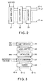
- the vertical driver 13 comprises, for example, a shift register 31, a level shifter 32, and a gate buffer 33, as shown in Fig.2 .
- the shift register 31 sequentially transfers the vertical start pulse VST, synchronized with a vertical clock VCK, to sequentially output it as a shift pulse from each transmission stage.
- the level shifter 32 boosts the shift pulse outputted from each transmission stage of the shift register 31 to supply it to the gate buffer 33.
- the gate buffer 33 sequentially supplies the shift pulse boosted in the level shifter 32 to the gate lines 17-1 to 17-m of the pixel section 12 as a vertical scanning pulse, and performs vertical scanning by selectively driving each pixel 11 of the pixel section 12 on the line basis.
- the horizontal driver 14 comprises a shift register 34, a level shifter 35, a data latch circuit 36, a D/A converter 37, and a buffer 38, as shown in Fig.3 .
- the shift register 34 sequentially transfers the horizontal start pulse HST, synchronized with a horizontal clock HCK, to sequentially output it as a shift pulse from each transmission stage and performs horizontal scanning.
- the level shifter 35 boosts the shift pulse outputted from each transmission stage of the shift register 34 to supply it to the data latch circuit 36.
- the data latch circuit 36 in response to the shift pulse supplied from the shift register 34 through the level shifter 35, sequentially latches supplied digital image data "data" of predetermined-bits.
- the D/A converter 37 is of a reference voltage selection type to convert the digital image data latched in the data latch circuit 36 to an analog image signal and supply it to the signal lines 18-1 to 18-n of the pixel section 12 through the buffer 38.
- the control system 15 for controlling the vertical driver 13 and the horizontal driver 14 comprises a timing controller (TC) 23, a reference voltage generating source 24, and a DC-CD converter 25. These circuits are mounted on the same substrate, that is, on the LCD panel 16, on which the pixel section 12 is mounted, together with the vertical driver 13 and the horizontal driver 14.
- the timing controller 23 receives power supply voltage VDD from an external power source section (not shown), digital image data "data” from an external CPU (not shown), and a clock CLK from an external clock generator (not shown) respectively through a TCP (tape carrier package), not shown.
- the CPU, a memory for storing image data and the clock generator are located outside of the LCD panel 16 in the present embodiment, at least one of them may be mounted on the LCD panel 16 as a part of the control system 15.
- the timing controller 23 performs timing control to supply the vertical start pulse VST, a clock signal such as the vertical clock VCK, and other kinds of control signals to the vertical driver 13, and also supplies the horizontal start pulse HST, a clock signal such as the horizontal clock HCK, other kinds of control signals, and the digital image data "data" to the horizontal driver 14.
- the reference voltage generating source 24 generates a plurality of reference voltages having different voltage values from one another, and supplies the plurality of reference voltage to the D/A converter 37 of the reference voltage selection type of the horizontal driver 14 as its reference voltage.
- the DC-DC converter 25 converts direct current voltage having low voltage (low voltage) into more than two kinds of high direct current voltage (high voltage) to supply them to each of the circuits such as the vertical driver 13, the horizontal driver 14, and the reference voltage generating source 24.
- transistors of the vertical driver 13 and the horizontal driver 14 are formed by a TFT, especially a poly-silicon TFT that is the same as the pixel transistor of the pixel section 12, on the same transparent insulating substrate on which the pixel section 12 is mounted and in an area of the transparent insulating substrate whose liquid crystal layer can be sealed by a sealing material.
- a TFT especially a poly-silicon TFT that is the same as the pixel transistor of the pixel section 12
- the movement range of the driving frequency of the vertical driver 13 and the horizontal driver 14 is limited to 10MHz or less.
- poly-silicon TFTs used as the pixel transistors of the pixel section 12 and the transistors constituting the driving system there are one having a bottom gate structure in which the gate electrode is arranged under an oxide film and one having a top gate structure in which the gate electrode is arranged on the oxide film.
- the cross-sectional structures of these poly-silicon TFTs are shown in Figs.4A and 4B .
- the TFT of the bottom gate structure shown in Fig.4A has a glass substrate 41, and the glass substrate 41 has formed thereon a plurality of gate electrodes 42.
- each of the gate electrodes 42 has formed thereon a gate oxide film 43 which bidirectionally extends to the glass substrate 41.
- the gate oxide film 43 has formed thereon a poly-silicon (Poly-Si) layer 44 upward from the gate electrode 42, and the poly-silicon layer 44 has formed thereon an inter-layer insulating film 45.
- the gate insulating film 43 has formed thereon at its side portions a source area 46 and a drain area 47 consisting of an N + diffusion layer.
- the source area 46 and the drain area 47 are connected to a source electrode 48 and a drain electrode 49, respectively.
- a poly-silicon layer 52 is formed on a glass substrate 51, on which a gate electrode 54 is formed via a gate oxide film 53, further on which an inter-layer insulating film 55 is formed. Also, on the glass substrate 51 on the side of the poly-silicon layer 52 are a source area 56 and a drain area 57 consisting of an N + diffusion layer, to which a source electrode 58 and a drain electrode 59 are respectively connected.
- the timing controller 23, the reference voltage generating source 24, and the DC-DC converter 25 of the control system 15 are integrated to be IC by single crystal silicon.
- This silicon IC is mounted by e.g., a COG (chip on glass) method on the same surface of the vertical driver 13 and the horizontal driver 14, that is, the substrate (transparent insulating substrate) on which the drivers 13 and 14 are formed.
- the silicon IC formed by the single crystal silicon can be driven in 100MHz.
- the poly-silicon TFT As described above, as the poly-silicon TFT is used to configure the vertical driver 13, the horizontal driver 14, that are the circuits which drive at low speed and have significant characteristics dispersion, the circuits using the poly-silicon TFT are sealed in a closed space of the pixel section 12. Thus, mixing of Na + ion, etc. causing the Vth (voltage at a threshold value) of the TFT can be prevented, which increases the reliability.
- the TFT is thin enough to be able to be ignored, compared with the liquid crystal cell (liquid crystal layer). Thus, it cannot be a cause to increase the thickness of the liquid crystal display device itself.
- the circuits which drive at high speed and have small characteristics dispersion this is, the timing controller 23, the reference voltage generating source 24, and the DC-DC converter 25 of the control system 15 are integrated to be IC by single crystal silicon, and are mounted on the same surface on which the vertical driver 13 and the horizontal driver 14 are formed.
- the cross-sectional view of this case is shown in Fig.5 .
- the liquid crystal display device includes a transparent insulating substrate 61 which has formed thereon the vertical driver 13 and so on, a transparent insulating substrate (facing substrate) 62 which faces the transparent insulating substrate 61, and a liquid crystal layer 63 held therebetween and sealed by a sealing material 64, as described above.
- an IC chip 65 into which the control system 15 is integrated is mounted by the COG method on the transparent insulating substrate 61 on which the vertical driver 13 and so on are mounted.
- Fig.6 shows a structure of an electric connection part between the circuit portion on the transparent insulating substrate 61 and the IC chip 65.
- a circuit portion 652 is formed on a silicon substrate 651, and the circuit portion 652 is electrically connected to an external connection terminal (bump material) 653.
- the external connection terminal 653 is electrically connected with a circuit wiring such as an aluminum wiring 611 on the transparent insulating substrate 61 via an anisotropic conducting film 66.
- an interlayer insulating film 67 exists between the transparent insulating substrate 61 and the IC chip 65.
- the IC chip 65 When the IC chip 65 is mounted on the transparent insulating substrate 61 as such, the IC chip 65 itself does not have a problem with respect to its reliability since a protective layer is formed on a silicon IC at the time of preparing the IC. Meanwhile, as it is in the COG structure, it is necessary to increase the reliability to a metal material of the connection portion with the transparent insulating substrate 61. To do this, after the IC chip 65 is formed on the transparent insulating substrate 61, a protective layer may be formed by silicon resin so that it may cover the IC chip 65 and the substrate 61.
- the IC chip 65 is formed so that its thickness t1 (about 0.7 mm) should be the thickness t3 of the facing transparent insulating substrate 62 and the sealing material 64 or thinner.
- the thickness t2 of the whole liquid crystal display device does not depend on the thickness t1 of the IC chip 65, it is possible to reduce the thickness of the liquid crystal display device. That is, the entire thickness t2 of the transparent insulating substrate 61, the transparent insulating substrate 62, and the sealing material 64 is the thickness of the liquid crystal display device itself.
- the peripheral circuits are integrated on chips, and the IC chip 65 is mounted on the transparent insulating substrate 61, the portions to be electrically connected to the external circuits of the LCD panel 16 can be reduced. Thus, it is possible to improve the reliability toward mechanical vibration of the LCD panel 16, and to refrain from generating the defection of electric connection in the manufacturing process.
- the mechanical strength of the IC chip 65 mounted by the COG method tends to be lower than the adhesive strength of the portion forming the liquid crystal cell of the pixel section 12.
- the thickness t1 of the IC chip 65 to be the total thickness t3 of the transparent insulating substrate 62 and the sealing material 64 or thinner, preferably thinner than the thickness t3, the IC chip 65 can be configured so that it is rarely forced from outside.
- organic materials such as PET (polyethylene terephtalate), PES (polyethersulfone), and so on are used as substrate materials for the transparent insulating substrates 61 and 62.
- the combination of the substrate materials for the transparent insulating substrates 61 and 62 there may be four cases in the following.
- silicon oxide is used as the substrate materials for both of the transparent insulating substrates 61 and 62.
- silicon oxide is used as the substrate material for the transparent insulating substrate 61
- the organic material such as PET, PES, or the like is used as the substrate material for the transparent insulating substrate 62.
- the organic material such as PET, PES, or the like is used as the substrate materials for both of the transparent insulating substrates 61 and 62.
- the organic material such as PET, PES, or the like is used as the substrate material for the transparent insulating substrate 61
- silicon oxide is used as the substrate material for the transparent insulating substrate 62.
- the combination in the case 3 in which the organic material such as PET, PES, or the like is used as the substrate materials for both of the transparent insulating substrates 61 and 62, is the most effective to reduce the thickness and lose the weight of the liquid crystal display device itself because the materials are extremely light in weight.
- the present invention is not limited to it, but can be applied to an active matrix type liquid crystal display device in so-to-speak a time-division driving system (selector system) described in the following.
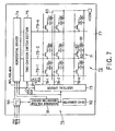
- Fig.7 is a schematic view showing a configuration example of an active matrix type liquid crystal display device in a time-division driving system to which the present invention is applied.
- the active matrix type liquid crystal display device in the time-division driving system has a configuration in which a pixel section 72 structured by arranging a number of pixels 71 in a matrix form, a vertical driver 73 which sequentially selects each of the pixels 71 of the pixel section 72 for each line, a horizontal driver 74 which writes pixel signals on each pixel 71 selected for each line, a time-division switch section 75 for time-division driving, and a control system 76 which controls the drivers 73 and 74 and the time-division switch section 75 are mounted on an LCD panel 77.
- Each of the pixel 71 is comprised of a poly-silicon TFT 80 in which its gate electrode is connected to each of the gate lines 78-1 to 78-m, and its source electrode is connected to each of the signal lines 79-1 to 79-n, a liquid crystal cell 81 connected at a pixel electrode to a drain electrode of the TFT 80, and an auxiliary capacity 82 connected at one electrode to the drain electrode of the TFT 80.
- the facing electrode of the liquid crystal cell 81 is connected to a common line 83, as well as the other electrode of the auxiliary capacity 82.
- To the common line 83 is provided with predetermined direct-current voltage as common voltage VCOM.
- the time-division driving system is a driving system in which a plurality of signal lines in the pixel section 72 adjacent to one another are divided into 1 unit (block), signal voltage supplied to the plurality of signal lines within the divided 1 block is outputted in time series from each of the output terminal of the horizontal driver 74, the time-division switch section 75 is provided with the plurality of signal lines being 1 unit, and the time-division switch section 75 time-divisionally samples the time-series signal voltage outputted from the horizontal driver 74 to sequentially supply it to each of the plurality of signal lines.
- the horizontal driver 74 outputs signal voltage to the plurality of signal lines in time series, with the plurality of signal lines being 1 unit.
- One example of the configuration of the horizontal driver 74 is shown in Fig.8 .
- the horizontal driver 74 comprises a shift register 84, a set of sampling switches 85, a level shifter 86, a data latch circuit 87, and a D/A converter 88, as shown in Fig.8 .
- the horizontal driver 74 takes in 5-bit digital image data, data 1 to data 5, and power supply voltage Vdd, Vss from both sides in a shift direction of the shift register 84.
- the shift register 84 sequentially transmits the horizontal start pulse HST, synchronized with a horizontal clock HCK, to sequentially output it as a shift pulse from each transmission stage and performs horizontal scanning.
- Each of the sampling switches in the set of sampling switches 85 sequentially sample the inputted digital image data, data 1 to data 5, in response to the shift pulse (sampling pulse) sequentially outputted from the shift register 84.
- the level shifter 86 boosts, for example, the 5V digital data sampled in the set of sampling switches 85 into digital data of liquid crystal driving voltage.
- the data latch circuit 87 is a memory for storing the digital data boosted in the level shifter 86 for 1H.
- the D/A converter 88 adopts a constitution of a reference voltage selection type to convert the digital image data for 1H outputted from the data latch circuit 87 to an analog image signal for output.
- the horizontal driver 74 one in a so-to-speak column inversion driving method is used.
- the horizontal driver 74 outputs signal voltage whose potential is inverted at each output terminal depending on whether it is odd or even, and inverts the polarity of the signal voltage at every field.
- the column inversion driving method is a driving method in which the pixels adjacent to one another in a vertical direction has the same polarity, and the state of the pixel polarity is inverted at every field. It is noted that the horizontal driver 74 can cope with a 1H common (VCOM) inversion driving.
- VCOM 1H common
- the time-division switch section 75 is configured by analog switches (transmission switches) which time-divisionally sample the time-series signal voltage outputted from the horizontal driver 74.
- analog switches transmission switches
- FIG.9 An example of a concrete configuration of the time-division switch section 75 is shown in Fig.9 . It is noted that the time-division switch section 75 is provided for each output of the horizontal driver 74. In this example, a three-timing division driving is performed in correspondence with R (red), G (green), and B (blue).
- the time-division switch section 75 is constituted by analog switches 75-1,75-2, and 75-3 in a CMOS configuration in which a PchMOS transistor and a NchNOS transistor are connected in series. Meanwhile, although the switches in the CMOS configuration are used as the analog switches 75-1, 75-2, and 75-3 in this example, the ones in a PMOS or NMOS configuration may also be used.
- the input terminals of the three analog switches 75-1, 75-2, and 75-3 are connected in common, and each of the output terminals are connected to one terminal of each of the three signal lines 79-1, 79-2, and 79-3.
- To each input terminal of the signal lines 79-1, 79-2, and 79-3 is supplied signal potential outputted in time series from the horizontal driver 74.
- control lines 89-1 to 89-6 in total are wired, two per one analog switch.
- Two control input terminals of the analog switch 75-1 that is, gates of the CMOS transistors, are connected to the control lines 89-1 and 89-2
- two control input terminals of the analog switch 75-2 are connected to the control lines 89-3 and 89-4
- two control input terminals of the analog switch 75-3 are connected to the control lines 89-5 and 89-6, respectively.
- gate selection signals S1 to S3 for sequentially selecting the three analog switches 75-1, 75-2, and 75-3 from a timing controller (TC) 90 (refer to Fig.7 ) described later.
- the gate selection signals XS1 to XS3 are inversion signals of the gate selection signals S1 to S3.
- the gate selection signals S1 to S3, XS1 to XS3 sequentially switch on the three analog switches 75-1, 75-2, and 75-3, synchronized with the time-series signal potential outputted from the horizontal driver 74. Accordingly, the three analog switches 75-1, 75-2, and 75-3 sample the time-series signal potential outputted from the horizontal driver 74 into three-timing divisions for 1H period, and supply them to corresponding signal lines 79-1, 79-2, and 79-3, respectively.
- the control system 76 which controls the drivers 73 and 74 and the time-division switch section 75 includes the timing controller (TC) 90, a reference voltage generating source 91, and a DC-DC converter 92, and these circuits are mounted on the same substrate on which the pixel section 72 is mounted, that is, the LCD panel 77, together with the drivers 73 and 74 and the time-division switch section 75.
- TC timing controller
- a reference voltage generating source 91 a reference voltage generating source
- DC-DC converter 92 DC-DC converter
- control system 76 to the timing controller 90 are inputted power supply voltage VDD from an external power source section (not shown), digital image data "data" from an external CPU (not shown), and a clock CLK from an external clock generator (not shown) respectively through a TCP (not shown).
- the CPU, a memory for storing image data, or the clock generator are provided outside of the LCD panel 77 in the present embodiment, at least one of them may be a part of the control system 76, integrated into a single crystal silicon IC (COG), and mounted on the LCD panel 77.
- COG single crystal silicon IC
- a memory for storing image data, or the clock generator at least one of a variety of control circuits such as a light source control circuit for an LCD, a graphic controller for displaying the LCD (or EL), and further a transceiver circuit, a battery control circuit, etc. in a case of using the present display device as a display section of, e.g., a portable telephone as will be described later may be integrated to be a single crystal silicon IC as a part of the control system 76 and mounted on the LCD panel 77.
- the light source control circuit for an LCD is a circuit for controlling a back light or a front light of the LCD, and does not supply power to a light source (light emitting diode, fluorescence display tube) at the time of a standby state of the portable telephone, but supplies power at the time of an input operation of the portable telephone.
- the graphic controller for displaying the LCD (or EL) is a circuit for converting image data supplied from the transceiver circuit into an image format so that the image data can be displayed in the image area of the LCD or the EL, converts into a display format of 160 pixels in a horizontal direction x 160 pixels in a vertical direction.
- the transceiver circuit is one for transmission, which receives digital signals and analog signals transmitted as electromagnetic wave and converts them to digital signals and analog signals as electric signals for output.
- the battery control circuit automatically lowers the operations of the clocks of the CPU, the LCD (or EL) panel, the graphic controller after a predetermined time period to lower the power consumption.
- the CPU when the display device is used as a display section of the portable telephone, the CPU also has a function to convert inputted information at the time of operating buttons in a case of the portable telephone into digital data.
- the timing controller 90 controls the timing, and supplies the vertical start pulse VST, a clock signal such as the vertical clock VCK, and other kinds of control signals to the vertical driver 73, also supplies the horizontal start pulse HST, a clock signal such as the horizontal clock HCK, other kinds of control signals, and the digital image data "data" to the horizontal driver 74, and also supplies the aforementioned fate selection signals S1 to S3, XS1 to XS3 to the time-division switch section 75, respectively.
- the reference voltage generating source 91 generates a plurality of reference voltage having different voltage values to one another, and supplies the plurality of reference voltage to the D/A converter 87 of the reference voltage selection type of the horizontal driver 74 as its reference voltage.
- the DC-DC converter 92 converts direct current voltage having low voltage (low voltage) into more than two kinds of high direct current voltage (high voltage) to supply them to each of the circuits such as the vertical driver 73, the horizontal driver 74, the reference voltage generating source 91, and so on.
- transistors included in the vertical driver 13 and the horizontal driver 14 and each of the analog switches consisting of the time-division switch section 75 are formed by a TFT, especially a poly-silicon TFT that is the same as the pixel transistor of the pixel section 72, on the same transparent insulating substrate on which the pixel section 72 is mounted and in an area in which the liquid crystal layer is sealed by a sealing material.
- the timing controller 90, the reference voltage generating source 91, and the DC-DC converter 92 of the control system 76 are integrated to be IC by single crystal silicon.
- This silicon IC is mounted by e.g., a COG method on the same surface of the vertical driver 73 and the horizontal driver 74, that is, the substrate on which the drivers 73 and 74 are formed.
- the poly-silicon TFT is used to configure the vertical driver 73, the horizontal driver 74, and the time-division switch section 75, that are the circuits which drive at low speed and have significant characteristics dispersion
- the circuits which drive at high speed or the circuits which have small characteristics dispersion, that is, the timing controller 90, the reference voltage generating source 91, and the DC-DC converter 92 of the control system 76 are integrated to be IC by single crystal silicon, and are mounted on the same surface on which the vertical driver 73 and the horizontal driver 74 are formed.
- the display device can obtain similar effects as the active matrix type liquid crystal display device in the analog point sequential driving system does.
- the timing controller 90, the reference voltage generating source 91, and the DC-DC converter 92 are mounted on the side of the vertical driver 2 in the present embodiment, the timing controller 90, the reference voltage generating source 91, and the DC-DC converter 92 may be integrated to be a single crystal silicon IC (COG) 98, integrally with the horizontal driver 74, and the IC 98 may be mounted on the LCD panel 77, as shown in Fig.10 .
- COG single crystal silicon IC
- the area for the space occupied by the timing controller 90, the reference voltage generating source 91, and the DC-DC converter 92 becomes unnecessary on the side of the vertical driver 72, and thus the frame width of the LCD panel 77 in a horizontal direction can be reduced for the occupied area.
- this is useful when this embodiment is applied to a display device having a specification in which the frame width in a horizontal direction is desired to be reduced.
- control circuits such as the light source control circuit for the LCD, the graphic controller for displaying the LCD (or EL), the transceiver circuit for a telephone, and the battery control circuit, etc. may be integrated to be a single crystal silicon IC, integrally with the horizontal driver 74.
- the display device is applicable to a display section of a portable terminal device such as a portable telephone, a PDA (personal digital assistant), etc. whose thickness is attempted to be thin, as well as to a display of an OA device such as a personal computer, a word processor, etc. and a television receiver.
- a portable terminal device such as a portable telephone, a PDA (personal digital assistant), etc. whose thickness is attempted to be thin
- a display of an OA device such as a personal computer, a word processor, etc. and a television receiver.
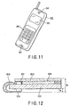
- Fig.11 is a perspective view showing an outward appearance of a portable terminal device to which the present invention is applied, for example, a portable telephone.
- the portable telephone of the present embodiment is constituted by arranging a speaker 94, a display section 95, an operation section 96, and a microphone 97 in order from the upper portion at the front surface of a device casing 93.
- a liquid crystal display device for example, is used for the display section 95, and the above-mentioned liquid crystal display device according to the present invention is used as this liquid crystal display device.
- the liquid crystal display device As the liquid crystal display device according to the present invention is used as the display section 95 in the portable terminal device such as the portable telephone, the liquid crystal display device has an advantage of being able to contribute to reducing the thickness of the portable terminal device itself since it is configured to be able to reduce the thickness of the portable terminal device itself.
- the semiconductor chip as the control system for controlling the driving system, is formed on the substrate on which the driving system is formed, the thickness of the whole display device does not depend on the thickness of the semiconductor chip. Thus, it can be realized to reduce the thickness of the whole display device and also to reduce the thickness of the portable terminal device that uses the device as a display section.
Abstract
Claims (9)
- Dispositif d'affichage comprenant :- un premier substrat (61) sur lequel est formée une section de pixels (12 ; 72) dans laquelle une pluralité de pixels (11 ; 71) est disposée sous une forme matricielle, un système d'attaque (13, 14 ; 73, 74) pour écrire des signaux de pixels dans la section de pixels et un système de commande (15 ; 76), qui est une puce semi-conductrice (65), pour commander ledit système d'attaque (13, 14 ; 73, 74) ;- ledit système d'attaque comprenant au moins un circuit d'attaque verticale (13 ; 73) et un circuit d'attaque horizontale (74) ;- ledit système de commande (15 ; 76) ayant au moins un contrôleur de synchronisation (23 ; 90), une source de génération de tension de référence (24 ; 91) et un convertisseur continu-continu (25 ; 92) ;- ledit convertisseur continu-continu (25 ; 92) étant apte à convertir une faible tension continue en plus de deux sortes de tensions continues élevées pour les envoyer au moins au circuit d'attaque verticale (13 ; 73), au circuit d'attaque horizontale (14 ; 74) et à la source de génération de tension de référence (24 ; 91) ;- un deuxième substrat (62) disposé en regard du premier substrat (61), avec un espace prédéterminé maintenu entre eux ;- une couche de matériau (63) retenue entre le premier substrat (61) et le deuxième substrat (62) pour générer des effets électro-optiques ;- un matériau d'étanchéité (64) disposé entre ledit premier substrat (61) et le deuxième substrat (62) ;- la puce semi-conductrice (65) étant formée sur la même surface que celle sur laquelle est formé le système d'attaque (13, 14 ; 73, 74), et l'épaisseur t1 de la puce semi-conductrice (65) étant définie de façon à ne pas être supérieure à une épaisseur t3 égale à la somme de l'épaisseur du matériau d'étanchéité (64) et de l'épaisseur du deuxième substrat (62).
- Dispositif d'affichage selon la revendication 1, dans lequel des transistors de type transistor à couche mince jouent le rôle de transistors de pixels de la section de pixels (11 ; 71) et de transistors composant le système d'attaque (13, 14 ; 73, 74).
- Dispositif d'affichage selon la revendication 2, dans lequel le transistor à couche mince est constitué de silicium polycristallin.
- Dispositif d'affichage selon la revendication 2, dans lequel le transistor à couche mince et la couche de matériau (63) sont enfermés de manière étanche entre le premier substrat (61) et le deuxième substrat (62).
- Dispositif d'affichage selon la revendication 1, dans lequel la puce semi-conductrice (65) est montée par un procédé COG.
- Dispositif d'affichage selon la revendication 1, dans lequel au moins l'un ou l'autre du premier substrat (61) et du deuxième substrat (62) est constitué d'un oxyde de silicium ou d'un matériau organique.
- Dispositif d'affichage selon la revendication 1, dans lequel la couche de matériau (63) est une couche de cristal liquide.
- Dispositif d'affichage selon la revendication 1, dans lequel la couche de matériau (63) est une couche électroluminescente.
- Dispositif terminal portable comprenant ledit dispositif d'affichage selon l'une quelconque des revendications 1 à 8 en tant que section d'affichage (95).
Applications Claiming Priority (3)
| Application Number | Priority Date | Filing Date | Title |
|---|---|---|---|
| JP2000171700 | 2000-06-08 | ||
| JP2000171700A JP4649706B2 (ja) | 2000-06-08 | 2000-06-08 | 表示装置およびこれを用いた携帯端末 |
| PCT/JP2001/004815 WO2001095298A1 (fr) | 2000-06-08 | 2001-06-07 | Ecran et assistant numerique personnel a ecran |
Publications (3)
| Publication Number | Publication Date |
|---|---|
| EP1248249A1 EP1248249A1 (fr) | 2002-10-09 |
| EP1248249A4 EP1248249A4 (fr) | 2005-06-22 |
| EP1248249B1 true EP1248249B1 (fr) | 2012-08-15 |
Family
ID=18674218
Family Applications (1)
| Application Number | Title | Priority Date | Filing Date |
|---|---|---|---|
| EP01936896A Expired - Lifetime EP1248249B1 (fr) | 2000-06-08 | 2001-06-07 | Afficheur |
Country Status (8)
| Country | Link |
|---|---|
| US (1) | US7193677B2 (fr) |
| EP (1) | EP1248249B1 (fr) |
| JP (1) | JP4649706B2 (fr) |
| KR (2) | KR100886885B1 (fr) |
| CN (1) | CN1286078C (fr) |
| NO (1) | NO326236B1 (fr) |
| TW (1) | TWI288288B (fr) |
| WO (1) | WO2001095298A1 (fr) |
Families Citing this family (21)
| Publication number | Priority date | Publication date | Assignee | Title |
|---|---|---|---|---|
| KR20030068415A (ko) * | 2002-02-14 | 2003-08-21 | 샤프 가부시키가이샤 | 표시장치, 전자기기 및 카메라 |
| TW200407834A (en) * | 2002-09-17 | 2004-05-16 | Seiko Epson Corp | Optoelectronic device, manufacturing method of optoelectronic device, and electronic machine |
| US20040125272A1 (en) * | 2002-12-30 | 2004-07-01 | Chung David B. | Flat panel display with polymer memory provided thereon |
| JP2005031661A (ja) * | 2003-06-20 | 2005-02-03 | Toshiba Matsushita Display Technology Co Ltd | 表示装置 |
| JP4651926B2 (ja) * | 2003-10-03 | 2011-03-16 | 株式会社 日立ディスプレイズ | 画像表示装置 |
| US20050083455A1 (en) * | 2003-10-16 | 2005-04-21 | Chung David B. | Spatially integrated display and memory system |
| US7427985B2 (en) | 2003-10-31 | 2008-09-23 | Au Optronics Corp. | Integrated circuit for driving liquid crystal display device |
| US7830348B2 (en) * | 2003-12-11 | 2010-11-09 | Au Optronics Corporation | Integrated circuit for liquid crystal display device |
| CN101031951B (zh) * | 2004-09-30 | 2012-04-04 | 富士通株式会社 | 液晶显示装置 |
| TWI288850B (en) * | 2005-02-04 | 2007-10-21 | Chi Mei Optoelectronics Corp | Display module and flat panel display device having the same |
| US20060232579A1 (en) * | 2005-04-14 | 2006-10-19 | Himax Technologies, Inc. | WOA panel architecture |
| TWI319553B (en) | 2005-05-13 | 2010-01-11 | Au Optronics Corp | Organic electro-luminescence display |
| EP1995787A3 (fr) * | 2005-09-29 | 2012-01-18 | Semiconductor Energy Laboratory Co, Ltd. | Dispositif de semi-conducteur disposant d'une couche de semi-conducteur d'oxyde et son procédé de fabrication |
| DE102006005677B4 (de) * | 2006-01-30 | 2015-12-31 | E.G.O. Elektro-Gerätebau GmbH | Kochfeld |
| JP5057321B2 (ja) | 2006-03-14 | 2012-10-24 | 株式会社ジャパンディスプレイウェスト | 表示装置の製造方法 |
| JP2009139774A (ja) * | 2007-12-10 | 2009-06-25 | Hitachi Displays Ltd | 表示装置 |
| TWI420480B (zh) * | 2009-05-19 | 2013-12-21 | Au Optronics Corp | 光電裝置及其顯示器 |
| JP5370189B2 (ja) * | 2010-02-04 | 2013-12-18 | セイコーエプソン株式会社 | 電気光学装置用基板、電気光学装置及び電子機器 |
| JP5664146B2 (ja) * | 2010-11-10 | 2015-02-04 | セイコーエプソン株式会社 | 情報表示端末 |
| KR102197826B1 (ko) * | 2014-09-03 | 2021-01-05 | 삼성디스플레이 주식회사 | 표시장치 |
| CN106412379B (zh) * | 2016-09-20 | 2019-02-15 | 青岛海信电器股份有限公司 | 实现频率同步的控制方法、装置及液晶电视 |
Family Cites Families (25)
| Publication number | Priority date | Publication date | Assignee | Title |
|---|---|---|---|---|
| NL7906695A (nl) * | 1979-09-07 | 1981-03-10 | Philips Nv | Weergeefinrichting. |
| JPS60238817A (ja) * | 1984-05-12 | 1985-11-27 | Citizen Watch Co Ltd | 液晶表示装置 |
| US5849601A (en) * | 1990-12-25 | 1998-12-15 | Semiconductor Energy Laboratory Co., Ltd. | Electro-optical device and method for manufacturing the same |
| JP2791422B2 (ja) * | 1990-12-25 | 1998-08-27 | 株式会社 半導体エネルギー研究所 | 電気光学装置およびその作製方法 |
| JPH07134279A (ja) * | 1993-11-12 | 1995-05-23 | Sharp Corp | アクティブマトリクス型液晶表示装置 |
| JPH07209672A (ja) * | 1993-12-03 | 1995-08-11 | Semiconductor Energy Lab Co Ltd | 非発光型ディスプレーを有する電子装置 |
| JP3402400B2 (ja) * | 1994-04-22 | 2003-05-06 | 株式会社半導体エネルギー研究所 | 半導体集積回路の作製方法 |
| JPH0836190A (ja) * | 1994-07-21 | 1996-02-06 | Hitachi Ltd | 液晶表示装置 |
| JP3715996B2 (ja) * | 1994-07-29 | 2005-11-16 | 株式会社日立製作所 | 液晶表示装置 |
| JP3889066B2 (ja) * | 1994-11-05 | 2007-03-07 | 株式会社半導体エネルギー研究所 | 半導体装置の作製方法 |
| JP3593198B2 (ja) * | 1995-12-20 | 2004-11-24 | 株式会社半導体エネルギー研究所 | フラットパネル型ディスプレイ装置及び液晶パネル |
| KR100195501B1 (ko) * | 1995-11-30 | 1999-06-15 | 김영남 | 레치형 전송기를 이용한 평판 표시기 데이타 구동 장치 |
| US6040827A (en) * | 1996-07-11 | 2000-03-21 | Hitachi, Ltd. | Driver circuit, driver integrated circuit, and display device and electronic device using the driver circuit and driver integrated circuit |
| JPH10186393A (ja) * | 1996-12-19 | 1998-07-14 | Shin Etsu Polymer Co Ltd | 液晶表示パネルの表示検査用コネクタ及びその製造方法 |
| JPH1184425A (ja) * | 1997-09-05 | 1999-03-26 | Semiconductor Energy Lab Co Ltd | 電気光学装置 |
| US6388652B1 (en) * | 1997-08-20 | 2002-05-14 | Semiconductor Energy Laboratory Co., Ltd. | Electrooptical device |
| JPH1185111A (ja) * | 1997-09-10 | 1999-03-30 | Sony Corp | 液晶表示素子 |
| US5994174A (en) * | 1997-09-29 | 1999-11-30 | The Regents Of The University Of California | Method of fabrication of display pixels driven by silicon thin film transistors |
| JPH11265155A (ja) * | 1998-03-18 | 1999-09-28 | Toshiba Corp | 平面型表示装置用基板 |
| JPH11281994A (ja) * | 1998-03-31 | 1999-10-15 | Advanced Display Inc | 液晶表示装置 |
| JPH11326932A (ja) * | 1998-05-19 | 1999-11-26 | Fujitsu Ltd | 液晶表示装置 |
| JPH11338432A (ja) * | 1998-05-28 | 1999-12-10 | Advanced Display Inc | 液晶駆動ic |
| JPH11352516A (ja) * | 1998-06-09 | 1999-12-24 | Matsushita Electric Ind Co Ltd | アクティブマトリックス型液晶表示パネル |
| JP3258284B2 (ja) * | 1998-11-10 | 2002-02-18 | セイコーインスツルメンツ株式会社 | 半導体回路 |
| US6576926B1 (en) * | 1999-02-23 | 2003-06-10 | Semiconductor Energy Laboratory Co., Ltd. | Semiconductor device and fabrication method thereof |
-
2000
- 2000-06-08 JP JP2000171700A patent/JP4649706B2/ja not_active Expired - Fee Related
-
2001
- 2001-06-07 KR KR1020087006567A patent/KR100886885B1/ko not_active IP Right Cessation
- 2001-06-07 US US10/049,052 patent/US7193677B2/en not_active Expired - Lifetime
- 2001-06-07 KR KR1020027001378A patent/KR100882248B1/ko not_active IP Right Cessation
- 2001-06-07 TW TW090113833A patent/TWI288288B/zh not_active IP Right Cessation
- 2001-06-07 EP EP01936896A patent/EP1248249B1/fr not_active Expired - Lifetime
- 2001-06-07 WO PCT/JP2001/004815 patent/WO2001095298A1/fr active Application Filing
- 2001-06-07 CN CNB018022901A patent/CN1286078C/zh not_active Expired - Fee Related
-
2002
- 2002-02-07 NO NO20020608A patent/NO326236B1/no not_active IP Right Cessation
Non-Patent Citations (1)
| Title |
|---|
| SEMOS M J ET AL: "CHIP-ON-GLASS: MAKING SMALLER PRODUCTS A REALITY", ELECTRONIC PACKAGING AND PRODUCTION, CAHNERS PUBLISHING CO, NEWTON, MASSACHUSETTS, US, vol. 39, no. 4, 1 March 1999 (1999-03-01), pages 43/44,46, XP000805956, ISSN: 0013-4945 * |
Also Published As
| Publication number | Publication date |
|---|---|
| KR20080037724A (ko) | 2008-04-30 |
| KR100886885B1 (ko) | 2009-03-05 |
| KR20020020802A (ko) | 2002-03-15 |
| US7193677B2 (en) | 2007-03-20 |
| US20030112403A1 (en) | 2003-06-19 |
| NO20020608D0 (no) | 2002-02-07 |
| CN1286078C (zh) | 2006-11-22 |
| EP1248249A4 (fr) | 2005-06-22 |
| JP4649706B2 (ja) | 2011-03-16 |
| NO326236B1 (no) | 2008-10-20 |
| EP1248249A1 (fr) | 2002-10-09 |
| CN1386255A (zh) | 2002-12-18 |
| JP2001350421A (ja) | 2001-12-21 |
| TWI288288B (en) | 2007-10-11 |
| NO20020608L (no) | 2002-02-07 |
| WO2001095298A1 (fr) | 2001-12-13 |
| KR100882248B1 (ko) | 2009-02-06 |
Similar Documents
| Publication | Publication Date | Title |
|---|---|---|
| EP1248249B1 (fr) | Afficheur | |
| KR100829066B1 (ko) | 액정 표시 장치 및 이것을 사용한 전자 장치 | |
| US8860706B2 (en) | Display device | |
| US7561150B2 (en) | Liquid crystal driving circuit and liquid crystal display device | |
| EP1300826A2 (fr) | Dispositif d'affichage et dispositif semi-conducteur | |
| US11257409B1 (en) | Gate on array circuit | |
| US7548109B2 (en) | Voltage converter and display device comprising a voltage converter | |
| US20050156811A1 (en) | Display system and electronic equipment using the same | |
| US7561655B2 (en) | Shift register circuit and method of operating the same | |
| US6958716B2 (en) | Data processing circuit, display device, and mobile terminal | |
| JP2002287653A (ja) | 表示装置およびその製造方法、ならびに携帯端末およびその製造方法 | |
| KR100774895B1 (ko) | 액정 표시 장치 | |
| JP4232599B2 (ja) | レベル変換回路および表示装置 | |
| JP4877413B2 (ja) | 表示装置およびこれを用いた携帯端末 | |
| JP4288849B2 (ja) | アクティブマトリクス型表示装置およびこれを用いた携帯端末 | |
| US20020105493A1 (en) | Drive circuit for display apparatus | |
| JP2001265297A (ja) | 走査線駆動回路およびその走査線駆動回路を有する平面表示装置ならびにその駆動方法 | |
| JP2006098812A (ja) | 電気光学装置、その制御方法および電子機器 | |
| JP2006227455A (ja) | 表示装置 | |
| JPH11311804A (ja) | 液晶表示装置 | |
| JP2002175050A (ja) | アクティブマトリクス型表示装置およびこれを用いた携帯端末 |
Legal Events
| Date | Code | Title | Description |
|---|---|---|---|
| PUAI | Public reference made under article 153(3) epc to a published international application that has entered the european phase |
Free format text: ORIGINAL CODE: 0009012 |
|
| 17P | Request for examination filed |
Effective date: 20020610 |
|
| AK | Designated contracting states |
Kind code of ref document: A1 Designated state(s): AT BE CH CY DE DK ES FI FR GB GR IE IT LI LU MC NL PT SE TR |
|
| RBV | Designated contracting states (corrected) |
Designated state(s): DE FI FR GB NL SE |
|
| A4 | Supplementary search report drawn up and despatched |
Effective date: 20050506 |
|
| RIC1 | Information provided on ipc code assigned before grant |
Ipc: 7G 09F 9/00 A Ipc: 7G 02F 1/1368 B Ipc: 7G 02F 1/1362 B Ipc: 7G 09F 9/30 B Ipc: 7G 02F 1/13 B |
|
| APBN | Date of receipt of notice of appeal recorded |
Free format text: ORIGINAL CODE: EPIDOSNNOA2E |
|
| RAP1 | Party data changed (applicant data changed or rights of an application transferred) |
Owner name: SONY CORPORATION |
|
| APBR | Date of receipt of statement of grounds of appeal recorded |
Free format text: ORIGINAL CODE: EPIDOSNNOA3E |
|
| APBV | Interlocutory revision of appeal recorded |
Free format text: ORIGINAL CODE: EPIDOSNIRAPE |
|
| GRAP | Despatch of communication of intention to grant a patent |
Free format text: ORIGINAL CODE: EPIDOSNIGR1 |
|
| RTI1 | Title (correction) |
Free format text: DISPLAY DEVICE |
|
| GRAS | Grant fee paid |
Free format text: ORIGINAL CODE: EPIDOSNIGR3 |
|
| GRAA | (expected) grant |
Free format text: ORIGINAL CODE: 0009210 |
|
| AK | Designated contracting states |
Kind code of ref document: B1 Designated state(s): DE FI FR GB NL SE |
|
| REG | Reference to a national code |
Ref country code: GB Ref legal event code: FG4D |
|
| REG | Reference to a national code |
Ref country code: SE Ref legal event code: TRGR |
|
| REG | Reference to a national code |
Ref country code: DE Ref legal event code: R096 Ref document number: 60146985 Country of ref document: DE Effective date: 20121011 |
|
| REG | Reference to a national code |
Ref country code: NL Ref legal event code: T3 |
|
| REG | Reference to a national code |
Ref country code: DE Ref legal event code: R097 Ref document number: 60146985 Country of ref document: DE |
|
| REG | Reference to a national code |
Ref country code: DE Ref legal event code: R082 Ref document number: 60146985 Country of ref document: DE Representative=s name: MITSCHERLICH & PARTNER PATENT- UND RECHTSANWAE, DE |
|
| RAP2 | Party data changed (patent owner data changed or rights of a patent transferred) |
Owner name: JAPAN DISPLAY WEST INC. |
|
| PLBE | No opposition filed within time limit |
Free format text: ORIGINAL CODE: 0009261 |
|
| STAA | Information on the status of an ep patent application or granted ep patent |
Free format text: STATUS: NO OPPOSITION FILED WITHIN TIME LIMIT |
|
| REG | Reference to a national code |
Ref country code: NL Ref legal event code: SD Effective date: 20130620 |
|
| REG | Reference to a national code |
Ref country code: FR Ref legal event code: TP Owner name: JAPAN DISPLAY WEST INC., JP Effective date: 20130619 |
|
| 26N | No opposition filed |
Effective date: 20130516 |
|
| REG | Reference to a national code |
Ref country code: GB Ref legal event code: 732E Free format text: REGISTERED BETWEEN 20130627 AND 20130703 |
|
| REG | Reference to a national code |
Ref country code: DE Ref legal event code: R081 Ref document number: 60146985 Country of ref document: DE Owner name: JAPAN DISPLAY WEST INC., OGAWA, JP Free format text: FORMER OWNER: SONY CORPORATION, TOKIO/TOKYO, JP Effective date: 20120816 Ref country code: DE Ref legal event code: R081 Ref document number: 60146985 Country of ref document: DE Owner name: JAPAN DISPLAY WEST INC., OGAWA, JP Free format text: FORMER OWNER: SONY CORPORATION, TOKYO, JP Effective date: 20130610 Ref country code: DE Ref legal event code: R082 Ref document number: 60146985 Country of ref document: DE Representative=s name: MITSCHERLICH, PATENT- UND RECHTSANWAELTE, PART, DE Effective date: 20130610 Ref country code: DE Ref legal event code: R082 Ref document number: 60146985 Country of ref document: DE Representative=s name: MITSCHERLICH, PATENT- UND RECHTSANWAELTE PARTM, DE Effective date: 20130610 Ref country code: DE Ref legal event code: R081 Ref document number: 60146985 Country of ref document: DE Owner name: JAPAN DISPLAY WEST INC., JP Free format text: FORMER OWNER: SONY CORPORATION, TOKYO, JP Effective date: 20130610 Ref country code: DE Ref legal event code: R081 Ref document number: 60146985 Country of ref document: DE Owner name: JAPAN DISPLAY WEST INC., JP Free format text: FORMER OWNER: SONY CORP., TOKIO/TOKYO, JP Effective date: 20120816 Ref country code: DE Ref legal event code: R082 Ref document number: 60146985 Country of ref document: DE Representative=s name: MITSCHERLICH & PARTNER PATENT- UND RECHTSANWAE, DE Effective date: 20130610 |
|
| REG | Reference to a national code |
Ref country code: DE Ref legal event code: R097 Ref document number: 60146985 Country of ref document: DE Effective date: 20130516 |
|
| REG | Reference to a national code |
Ref country code: FR Ref legal event code: PLFP Year of fee payment: 16 |
|
| PGFP | Annual fee paid to national office [announced via postgrant information from national office to epo] |
Ref country code: FI Payment date: 20160613 Year of fee payment: 16 |
|
| PGFP | Annual fee paid to national office [announced via postgrant information from national office to epo] |
Ref country code: SE Payment date: 20160620 Year of fee payment: 16 |
|
| REG | Reference to a national code |
Ref country code: FR Ref legal event code: PLFP Year of fee payment: 17 |
|
| PGFP | Annual fee paid to national office [announced via postgrant information from national office to epo] |
Ref country code: DE Payment date: 20170621 Year of fee payment: 17 Ref country code: GB Payment date: 20170620 Year of fee payment: 17 Ref country code: FR Payment date: 20170621 Year of fee payment: 17 |
|
| PGFP | Annual fee paid to national office [announced via postgrant information from national office to epo] |
Ref country code: NL Payment date: 20170620 Year of fee payment: 17 |
|
| REG | Reference to a national code |
Ref country code: SE Ref legal event code: EUG |
|
| PG25 | Lapsed in a contracting state [announced via postgrant information from national office to epo] |
Ref country code: FI Free format text: LAPSE BECAUSE OF NON-PAYMENT OF DUE FEES Effective date: 20170607 |
|
| PG25 | Lapsed in a contracting state [announced via postgrant information from national office to epo] |
Ref country code: SE Free format text: LAPSE BECAUSE OF NON-PAYMENT OF DUE FEES Effective date: 20170608 |
|
| REG | Reference to a national code |
Ref country code: DE Ref legal event code: R119 Ref document number: 60146985 Country of ref document: DE |
|
| REG | Reference to a national code |
Ref country code: NL Ref legal event code: MM Effective date: 20180701 |
|
| GBPC | Gb: european patent ceased through non-payment of renewal fee |
Effective date: 20180607 |
|
| PG25 | Lapsed in a contracting state [announced via postgrant information from national office to epo] |
Ref country code: NL Free format text: LAPSE BECAUSE OF NON-PAYMENT OF DUE FEES Effective date: 20180701 |
|
| PG25 | Lapsed in a contracting state [announced via postgrant information from national office to epo] |
Ref country code: GB Free format text: LAPSE BECAUSE OF NON-PAYMENT OF DUE FEES Effective date: 20180607 Ref country code: FR Free format text: LAPSE BECAUSE OF NON-PAYMENT OF DUE FEES Effective date: 20180630 Ref country code: DE Free format text: LAPSE BECAUSE OF NON-PAYMENT OF DUE FEES Effective date: 20190101 |