EP1239308A2 - Polariseur à grille métallique - Google Patents
Polariseur à grille métallique Download PDFInfo
- Publication number
- EP1239308A2 EP1239308A2 EP02075711A EP02075711A EP1239308A2 EP 1239308 A2 EP1239308 A2 EP 1239308A2 EP 02075711 A EP02075711 A EP 02075711A EP 02075711 A EP02075711 A EP 02075711A EP 1239308 A2 EP1239308 A2 EP 1239308A2
- Authority
- EP
- European Patent Office
- Prior art keywords
- wire grid
- wire
- grid polarizer
- wires
- polarization
- Prior art date
- Legal status (The legal status is an assumption and is not a legal conclusion. Google has not performed a legal analysis and makes no representation as to the accuracy of the status listed.)
- Granted
Links
Images


Classifications
-
- G—PHYSICS
- G02—OPTICS
- G02B—OPTICAL ELEMENTS, SYSTEMS OR APPARATUS
- G02B5/00—Optical elements other than lenses
- G02B5/30—Polarising elements
- G02B5/3025—Polarisers, i.e. arrangements capable of producing a definite output polarisation state from an unpolarised input state
- G02B5/3058—Polarisers, i.e. arrangements capable of producing a definite output polarisation state from an unpolarised input state comprising electrically conductive elements, e.g. wire grids, conductive particles
-
- H—ELECTRICITY
- H01—ELECTRIC ELEMENTS
- H01Q—ANTENNAS, i.e. RADIO AERIALS
- H01Q15/00—Devices for reflection, refraction, diffraction or polarisation of waves radiated from an antenna, e.g. quasi-optical devices
- H01Q15/24—Polarising devices; Polarisation filters
Definitions
- the present invention relates to wire grid polarizers in general and in particular to multilayer wire grid polarizers and beamsplitters for the visible spectrum.
- Wire grids generally in the form of an array of thin parallel conductors supported by a transparent substrate, have also been used as polarizers for the infrared portion of the electromagnetic spectrum.
- the key factor that determines the performance of a wire grid polarizer is the relationship between the center-to-center spacing, sometimes referred to as period or pitch, of the parallel grid elements and the wavelength of the incident light. If the grid spacing or period is long compared to the wavelength, the grid functions as a diffraction grating, rather than as a polarizer, and diffracts both polarizations, not necessarily with equal efficiency, according to well-known principles. However, when the grid spacing (p) is much shorter than the wavelength, the grid functions as a polarizer that reflects electromagnetic radiation polarized parallel ("s" polarization) to the grid, and transmits radiation of the orthogonal polarization ("p" polarization).
- s electromagnetic radiation polarized parallel
- p orthogonal polarization
- the transition region where the grid period is in the range of roughly one-half of the wavelength to twice the wavelength, is characterized by abrupt changes in the transmission and reflection characteristics of the grid.
- an abrupt increase in reflectivity, and corresponding decrease in transmission, for light polarized orthogonal to the grid elements will occur at one or more specific wavelengths at any given angle of incidence.
- ⁇ ⁇ (n +/- sin ⁇ )/k
- epsilon ( ⁇ ) is the grating period
- n is the refractive index of the medium surrounding the grating
- k is an integer corresponding to the order of the diffracted term that is emerging
- lambda and theta are the wavelength and incidence angle (both measured in air) where the resonance occurs.
- the effect of the angular dependence is to shift the transmission region to larger wavelengths as the angle increases. This is important when the polarizer is intended for use as a polarizing beam splitter or polarizing turning mirror.
- a wire grid polarizer will reflect light with its electric field vector parallel ("s" polarization) to the wires of the grid, and transmit light with its electric field vector perpendicular (“p" polarization) to the wires of the grid, but the plane of incidence may or may not be perpendicular to the wires of the grid as discussed here.
- the wire grid polarizer will function as a perfect mirror for one polarization of light, such as the S polarized light, and will be perfectly transparent for the other polarization, such as the P polarized light. In practice, however, even the most reflective metals used as mirrors absorb some fraction of the incident light and reflect only 90% to 95%, and plain glass does not transmit 100% of the incident light due to surface reflections.
- wire grid polarizers and indeed other polarization devices, is mostly characterized by the contrast ratio, or extinction ratio, as measured over the range of wavelengths and incidence angles of interest.
- contrast ratios for the transmitted beam (Tp/Ts) and the reflected beam (Rs/Rp) may both be of interest.
- wire grid polarizers were developed for use in the infrared, but were unavailable for visible wavelengths. Primarily, this is because processing technologies were incapable of producing small enough sub-wavelength structures for effective operation in the visible spectrum. Nominally, the grid spacing or pitch (p) should be less than ⁇ /5 for effective operation (for p ⁇ 0.10-0.13 ⁇ m for visible wavelengths), while even finer pitch structures (p ⁇ /10 for example) can provide further improvements to device contrast.
- finer pitch structures p ⁇ /10 for example
- visible wavelength wire grid structures have become feasible.
- visible wavelength wire grid polarizers devices known in the art these devices do not provide the very high extinction ratios (>1,000:1) across broadband visible spectra needed for demanding applications, such as for digital cinema projection.
- a wire grid polarization beam splitter for the visible wavelength range is described by Hegg et al. in US Patent No. 5,383,053, in which the metal wires (with pitch p ⁇ and ⁇ 150 nm features) are deposited on top of metal grid lines, each of which are deposited onto glass or plastic substrate. While this device is designed to cover much of the visible spectrum (0.45-0.65 ⁇ m), the anticipated polarization performance is rather modest, delivering an overall contrast ratio of only 6.3:1.
- Tamada et al in U.S. Patent No. 5,748,368, describes a wire grid polarizer for the near infrared spectrum (0.8-0.95 ⁇ m) in which the structure of the wires is shaped in order to enhance performance.
- operation in near infrared spectrum is achieved with a wire structure with a long grid spacing ( ⁇ /2 ⁇ p ⁇ ) rather than the nominal small grid spacing (p ⁇ /5) by exploiting one of the resonances in the transition region between the wire grid polarizer and the diffraction grating.
- the wires, each ⁇ 140 nm thick are deposited on a glass substrate in an assembly with wedge plates.
- the device uses a combination of trapezoidal wire shaping, index matching between the substrate and a wedge plate, and incidence angle adjustment to tune the device operation to hit a resonance band. While this device provides reasonable extinction of ⁇ 35:1, which would be useful for many applications, this contrast in inadequate for applications, such as digital cinema, which require higher performance. Furthermore, this device only operates properly within narrow wavelength bands ( ⁇ 25 nm) and the device is rather angularly sensitive (a 2° shift in incidence angle shifts the resonance band by ⁇ 30 nm). These considerations also make the device unsuitable for broadband wavelength applications in which the wire grid device must operate in "fast" optical system (such as F/2).
- this device By using wires of ⁇ 0.13 ⁇ m grid spacing or pitch, this device has the required sub-visible wavelength structure to allow it to generally operate above the long wavelength resonance band and in the wire grid region.
- the '103 patent proposes a variety of improvements to the basic wire grid structure directed to broadening the wavelength spectrum and improving the efficiency and contrast across the wavelength spectrum of use without requiring finer pitch structures (such as ⁇ /10).
- a variety of techniques are employed to reduce the effective refractive index (n) in the medium surrounding the wire grid, in order to shift the longest wavelength resonance band to shorter wavelengths (see equations (1) and (2)). This is accomplished most simply by coating the glass substrate with a dielectric layer which functions as an anti-reflectional (AR) coating, and then fabricating the wire grid onto this intermediate dielectric layer.
- AR anti-reflectional
- the intermediate dielectric layer effectively reduces the refractive index experienced by the light at the wire grid, thereby shifting the longest wavelength resonance shorter.
- the '103 patent also describes alternate designs where the effective index is reduced by forming grooves in the spaces between the wires, such that the grooves extend into the substrate itself, and/or into the intermediate dielectric layer which is deposited on the substrate.
- the low wavelength band edge shifts ⁇ 50-75 nm lower, allowing coverage of the entire visible spectrum.
- the average efficiency is improved by ⁇ 5% across the visible spectrum over the basic prior art wire grid polarizer.
- the performance of these devices varies considerably across the visible spectrum, with the polarization beam splitter providing contrast ratios for the transmitted beam varying from ⁇ 300:1 to ⁇ 1200:1 from blue to red, while the reflected beam contrast ratios vary from 10:1 to 30:1.
- the polarization beam splitter provides contrast ratios for the transmitted beam varying from ⁇ 300:1 to ⁇ 1200:1 from blue to red, while the reflected beam contrast ratios vary from 10:1 to 30:1.
- a wire grid polarizer for polarizing an incident light beam comprises a substrate having a first surface.
- a grid or array of parallel, elongated, conductive wires is disposed on the first surface, and each of the adjacent wires are spaced apart on a grid period less than a wavelength of incident light.
- Each of the wires comprises an intra-wire substructure of alternating elongated metal wires and elongated dielectric layers.
- Figure 1 is a perspective view of a prior art wire grid polarizer.
- Figures 2a and 2b are plots illustrating the relative performance of prior art wire grid polarizers and polarization beamsplitters designed to operate within the visible spectrum.
- Figures 3a and 3b are plots of transmitted, reflected, and overall polarization contrast ratios vs. wavelength in the visible spectrum for a wire grid polarization beamsplitter of a type described in the prior art.
- Figure 4 is a contour plot of the overall contrast vs. angle of incidence for 500 nm light for a wire grid polarization beamsplitter of a type described in the prior art.
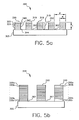
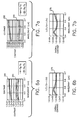
- Figures 5a-5d are sectional view of various configurations of the wire grid polarizer according to the present invention.
- Figures 6a and 6b are graphical plots illustrating a reflected and transmitted polarization contrasts ratio vs. wavelength, and the overall contrast ratio vs. wavelength for a wire grid polarizer of the present invention, where the device has a six layer structure.
- Figures 7a and 7b are graphical plots illustrating a reflected and transmitted polarization contrasts ratio vs. wavelength, and the overall contrast ratio vs. wavelength for a wire grid polarizer of the present invention, where the device has an eighteen layer structure.
- Figures 8a and 8b are graphical plots illustrating a reflected and transmitted polarization contrasts ratio vs. wavelength, and the overall contrast ratio vs. wavelength for a wire grid polarizer of the present invention, where the device has an alternate eighteen layer structure.
- Figures 9a and 9b are graphical plots illustrating a reflected and transmitted polarization contrasts ratio vs. wavlength, and the overall contrast ratio vs. wavelength for a wire grid polarizer of the present invention, where the device has a five layer structure.
- Figures 10a and 10b are graphical plots illustrating a reflected and transmitted polarization contrasts ratio vs. wavelength, and the overall contrast ratio vs. wavelength for a wire grid polarizer of the present invention, where the device has an alternate five layer structure.
- FIG. 1 illustrates a basic prior art wire grid polarizer and defines terms that will be used in a series of illustrative examples of the prior art and the present invention.
- the wire grid polarizer 100 is comprised of a multiplicity of parallel conductive electrodes 110 supported by a dielectric substrate 120. This device is characterized by the grating spacing or pitch or period of the conductors, designated p; the width of the individual conductors, designated w; and the thickness of the conductors, designated t.
- a wire grid polarizer uses sub-wavelength structures, such that the pitch (p), conductor or wire width (w), and the conductor or wire thickness (t) are all less than the wavelength of incident light ( ⁇ ).
- a beam of light 130 produced by a light source 132 is incident on the polarizer at an angle ⁇ from normal, with the plane of incidence orthogonal to the conductive elements.
- the wire grid polarizer 100 divides this beam into a specularly reflected light beam 140, and a non-diffracted, transmitted light beam 150.
- the normal definitions for S and P polarization are used, such that the light with S polarization has the polarization vector orthogonal to the plane of incidence, and thus parallel to the conductive elements. Conversely, light with P polarization has the polarization vector parallel to the plane of incidence and thus orthogonal to the conductive elements.
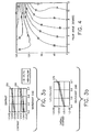
- the transmission efficiency curve 200 and the transmitted "p" polarization contrast ratio curve 205 for a commercially available wire grid polarization beam splitter from Moxtek Inc. of Orem UT.
- This device is similar to the basic wire grid polarization beam splitter described in the '131 patent, which has ⁇ 130 nm pitch (p ⁇ /5) wires (parallel conductive electrodes 110) made with a 40-60% duty cycle (52-78 nm wire width (w)) deposited on a dielectric substrate 120.
- the solid metal wires are defined to be >20 nm thick, which guarantees sufficient metal thickness that the skin depth ( ⁇ ) is exceeded for visible wavelengths.
- This data is representative for this device for a modest NA (numerical aperture) light beam, incident on the wire grid polarizer 100 at an angle of incidence ( ⁇ ) of 45°.
- this device divides the incident beam of light 130 into two outgoing polarized beams (140 and 150), which travel paths spatially distinguishable from the incoming light path, this device is considered to be a polarizing beam splitter.
- the transmitted contrast ratio curve 200 measures the average contrast of the transmitted "p" polarized light, relative to the transmitted "s" polarized light (Tp/Ts), where the "s" polarized light is undesirable leakage.
- the reflected contrast ratio curve 210 measures the average contrast of the reflected "s" polarized light relative to the "p” polarized light (Rs/Rp).
- the performance curves shown in figures 2a and 2b are very good relative to pre-existing wire grid devices, as well as pre-existing polarizers in general, there is yet room for improvement.
- the contrast ratio of the reflected "s" polarized beam is rather low, as measured by the reflected contrast ratio curve 210, for the wire grid polarizing beam splitter.
- Polarization contrast is only ⁇ 10:1 in the blue spectrum (at 450 nm), and even in the red (650 nm), it has risen only to ⁇ 40:1. In applications where both the reflected and transmitted beams need good polarization contrast, this performance is insufficient.
- the performance level of the basic wire grid polarizer can be improved by changing the width of the wires, the thickness of the wires, the pitch of the wires, or any combination of these three.
- these design changes may not necessarily provide contrast ratios desired for the reflected beam or across the required wavelength bands.
- the improvements in wire grid design performance described in the '103 patent, which broaden the wavelength pass band and increase transmission efficiency by modifying the interaction of the incident light with the dielectric substrate 120 will also not necessarily provide sufficient contrast ratios for broadband visible high contrast applications.
- the wire grid polarizers of the '131 and '103 patents, as well as the other cited prior art wire grid device patents only exploit resonance effects within the plane(s) of the elongated wires (X:Y plane of Figure 1), which comprise the wire grid polarizer or polarization beam splitter. As the incident light interacts with the wires and the dielectric substrate 120 simultaneously, the structural details at the interface also affect performance (as discussed in the '103 patent ). Thus the plane of the wires should be considered to include the wires themselves as well as the immediate surface and subsurface of the dielectric substrate 120.
- Figure 3a shows the calculated reflected and transmitted polarization contrast ratios as a function of wavelength for a device similar to the prior art wire grid polarization beamsplitter described in the '131 patent.
- This analysis was modeled using the Gsolver grating analysis software tool, which allows sub-wavelength structures to be thoroughly modeled using rigorous coupled wave analysis (RCWA).
- Gsolver is commercially available from Grating Solver Development Company, P.O. Box 353, Allen, Texas.
- the wire grid device was modeled as a series of parallel elongated wires formed directly on the transparent glass substrate.
- plot 250 of Figure 2a represents the angle averaged performance of an actual device
- plot 250 of Figure 3a represents the theoretical performance of a collimated beam though a perfect device
- Figure 3a also shows the theoretical reflected beam contrast 255 as modeled for this prior art type wire grid devices.
- the calculated theoretical reflected beam contrast ranges from ⁇ 10:1 to ⁇ 100:1 over the visible spectrum, and is only marginally better than the reflected beam contrast 255 given in Figure 2a for an actual device.
- the overall contrast C which combines the contrast of the transmitted light beam 150 ("p" polarization) with the contrast of the reflected light beam 140 ("s" polarization), can be seen to be mostly determined by the lowest contrast ratio, which is the contrast for the reflected light beam.
- the overall contrast of the prior art type device per the '131 patent is limited by the "s" polarization reflected beam, and is only ⁇ 10:1 to ⁇ 100:1 within the visible spectrum, with the lowest performance for blue wavelengths.
- Figure 4 shows the modeled variation of the overall contrast ratio C as contour lines vs. angle at 500 nm for this same prior art type device (0,0 coordinate corresponds to 45°). This shows that the overall contrast ratio 275 varies significantly with incidence angle, from ⁇ 23:1 at 45° incidence, to ⁇ 14:1 at ⁇ 55° incidence (polar angle +10°) to ⁇ 30:1 at ⁇ 35° incidence (polar angle +10°, azimuthal angle 180°). Thus Figure 4 effectively shows how the overall contrast ratio is average lower by having large NA incident beams of light. Of course, the overall contrast C is limited by the reflected contrast (Rs/Rp). A similar analysis of just the transmitted beam contrast (Tp/Ts) vs.
- Wire grid polarizer 300 of the present invention employs a construction wherein each of the elongated composite wires 310 (or parallel conductive electrodes) has a stratified internal structure comprised of a series of elongated metal wires (320, 322, 324) and alternating elongated dielectric strips (dielectric layers 340,342, 344) deposited on a transparent dielectric substrate 305.
- a combination of photon tunneling and the intra-grid resonance effects can be exploited to enhance the performance of the polarizer.
- the wire grid polarizers of the present invention not only uses resonance effects within the plane (X:Y plane) of the elongated wires, but also uses resonance effects between multiple parallel intra-wire planes along the Z axis to define and enhance the performance.
- the wire grid polarizers 300 depicted in Figure 5a-d are not to scale illustrations, and the composite wires 310 are exaggerated to show the intra-wire substructure of elongated metal wires alternating with dielectric layers.
- the pitch (p) and the wire width (w) are sub-wavelength in dimension ( ⁇ /5 or smaller).
- the wire thickness (t) is also nominally sub-wavelength as well, although not necessarily so, as will be discussed.
- the design of the wire grid polarizers of the present invention is based upon the use of a little known physical phenomena, resonance enhanced tunneling, in which properly constructed metal layers can be partially transparent to incident light.
- This phenomena which occurs when a photonic band gap structure is constructed which enables resonance enhanced tunneling, is described in the literature, for example in a survey article "Photonic Band Gap Structure Makes Metals Transparent” in OE Reports, Dec. 1999, pg. 3.
- the concepts are also described in greater detail in the article "Transparent, Metallo-Dielectric, One-Dimensional, Photonic Band-Gap Structures" in J. App. Phys. 83 (5), pp. 2377-2383, 1 March 1998, by M. Scalora et al.
- ⁇ ⁇ / 4 ⁇ n i , where the calculated depth corresponds to the distance at which the light intensity has decreased to ⁇ 1/e 2 of its value at the input surface (where n i is the imaginary part of the refractive index).
- n i is the imaginary part of the refractive index.
- thin metal layers are considered opaque relative to transmitted visible light when their thicknesses exceed the typical skin depth values ⁇ , of only 10-15 nm, for metals such as aluminum and silver.
- a metallo-dielectric photonic band gap structure can be constructed with alternating layers of thin metal sheets and thin dielectric sheets, such that the incident light can be efficiently transmitted through individual metal layers which are thicker than the skin depth ⁇ .
- a photonic band gap structure is a structure with alternating layers of materials or sections of similar thicknesses having different indices of refraction which are periodically or quasi-periodically spaced on a substrate or other structure.
- these structures can be imagined by considering any single composite wire 310 of Figure 5a, and its constituent alternating metal wires (320,322,324) and dielectric layers (340,342,344) as being stretched into a sheet to cover much of the two dimensional surface of the dielectric substrate 305.
- one three period structure described in these articles which has three 30 nm thick aluminum (A1) layers separated by three 140 nm thick magnesium fluoride layers (MgF2), provides a variable 15-50% transmission in the green wavelength band.
- incident light tunnels through the first thin metallic layer, and evanescently encounters the following dielectric layer.
- the light transmitted through the first metal layer into the following dielectric layer encounters the second metal layer.
- the proper boundary conditions are then established such that the overall structure acts much like a Fabry-Perot cavity (or Etalon) and resonance in the dielectric layer enhances light transmission through the metal layers.
- the resonance enhanced tunneling effect is then further enhanced by the repeated design of the structure, with alternating thin metallic and thin dielectric layers.
- these articles show that adding more periods (and thus adding to the total metal thickness) can increase total light transmission vs. structures with fewer periods, as well as reduce the oscillations within the bandpass region. Furthermore, it is shown that adjustment of the dielectric layer thicknesses can shift the edges of the bandpass structure towards longer or shorter wavelengths, depending on the changes made.
- the thin dielectric layers in these structures are significantly thicker than the thin metal layers ( ⁇ 3-10x or greater), while the thin metal layers may be only a skin depth thick, but may also be several times thicker than the theoretical skin depth ( ⁇ ).
- the prior art does not foresee the benefit of applying the resonance enhanced tunneling of metallo-dielectric photonic bandgap structures to the design of polarization devices generally, or to wire grid polarizers and polarization beam splitters in particular. Moreover, it is not necessarily clear that the resonance enhanced tunneling effect would improve the performance of a wire grid polarization device by improving polarization contrast or transmission across the entire visible spectrum, or even any single color band.
- the wire grid polarizers 300 of the present invention use a plurality of identically fabricated elongated composite wires 310, each with an intra-wire substructure comprising alternating metal wires (320, 322, 324) and dielectric layers (340, 342, 344).
- alternating metal wires 320, 322, 324
- dielectric layers 340, 342, 344.
- the wire grid polarizers of the present invention effectively constructs each wire as a series of alternating thin metal layer and dielectric layers.
- the incident light of polarization orthogonal to the wires is transmitted in part through the metallic layers themselves by photonic tunneling and enhanced resonance effects, and thus the overall contrast ratio of the transmitted polarized light vs. the reflected polarized light is enhanced.
- the wire grid polarization devices of the present invention also use resonance effects in the orthogonal direction (the Z direction of Figure 1) to determine the performance.
- each elongated composite wire 310 has a periodic stratified intra-wire structure 315 of six layers comprising alternating layers of metal (metal wires 320, 322, and 324) and dielectric (dielectric layers 340, 342, 344).
- wire grid polarizer 300 was modeled as a structure with the wires located on a 130 nm pitch (p ⁇ /5), with a duty cycle of 40 %, such that the width (w) of the wires is 52 nm.
- grooves 312 between composite wires 310 are 78 nm wide.
- Grooves 312 are nominally filled with air, rather than some other medium, such as an optical liquid or gel.
- composite wires 310 were modeled with an intra-wire structure 315 comprising three thin dielectric layers (dielectric layers 340, 342, 344) of MgF2, each 33 nm thick, alternating with three thin metal layers (metal wires 320, 322, and 324) of aluminum, each 61 nm thick.
- incident light interacts with the effective index of each layer, where the effective index depends on the geometry of the composite wires 310, the geometry of the layer itself, the complex refractive index of the layer (either metal or dielectric), the refractive index of the material between the wires (air), and the boundary conditions established by the adjacent layers.
- the intra-wire structure is designed such that the third dielectric layer 344 is located in between the third metal wire 324 and surface 307 of transparent dielectric substrate 305.
- the total wire thickness (t) of the composite wires 310 which is the sum of the thicknesses of the three metal wires 320, 322, and 324 and the three dielectric layers 340, 342, 344, is 282 nm or ( ⁇ /2).
- the modeled polarization performance for this device which is shown in Figures 6a and 6b, is an improvement in both reflection and transmission to the basic wire grid polarizer whose modeled results were given in Figures 3a and 3b. Performance was modeled with Gsolver, using 8 diffraction orders, to ensure accuracy.
- the theoretical transmitted beam contrast 250 for "p" light varies from 10 5 -10 6 :1 across the visible spectrum, while the reflected beam contrast 255 for 's" light averages a fairly uniform ⁇ 100:1 across the visible spectrum.
- the overall contrast ratio 275 shown in Figure 6b, also averages ⁇ 100:1 across the entire visible spectrum.
- the improved polarization performance is not gained at the cost of efficiency, as the "s" light reflection efficiency is ⁇ 91%, while the "p" light transmission efficiency is ⁇ 83%, with little variation across the visible spectrum.
- this device could provide improved performance as a polarization beam splitter, in applications where both "p" and “s' polarized beams are to be used.
- this device also shows a ⁇ 10x improvement in the "p" polarized light contrast over the prior art device of the '131 patent, as well as an enhanced blue performance, with the reflected beam contrast 255 and the overall contrast ratio 275 averaging ⁇ 250:1 contrast over most of the blue spectrum.
- Such performance could be useful in many applications, including projection systems.
- a contour plot analysis of the overall contrast C showed that average contrast values of ⁇ 500:1 are obtained within a wide angular swath (+/-12° polar, and +/-30° azimuthal) at 500 nm.
- the transmitted beam contrast over the entire visible spectrum >10 5 :1 at normal incidence the first example wire grid polarizer was proven to function well as a polarization analyzer or polarizer, and not just as a wire grid polarization beam splitter.
- the '381 patent wire grid polarizer design preferentially locates adjacent wire grids with an inter-grid spacing (1) and pitch offset (p/2) so as to avoid the occurrence of inter-grid resonance or Etalon effects.
- the wire grid polarizers 300 of the present invention specifically use Etalon type resonance effects within stratified intra-wire substructure in order to enhance performance.
- each composite wire 310 has a periodic stratified intra-wire structure 315 of eighteen layers comprising alternating layers of metal (metal wires 330a-i) and dielectric (dielectric layers 350a-i).
- the second example wire grid polarizer 300 was modeled as a structure 130 nm pitch (p ⁇ /5) composite wires 310, with a 40% duty cycle wire width (w) of 52 nm.
- composite wires 310 were modeled with an intra-wire structure 315 comprising nine thin MgF2 dielectric layers (dielectric layers 330a-i), each 39 nm thick, alternating with nine thin aluminum metal layers (metal wires 350a-i), each 17 nm thick.
- the total wire thickness (t) of composite wires 310 which is the sum of thicknesses of metal wires 330a-i and dielectric layers 350a-i is 504 nm, which is ⁇ 1 ⁇ .
- the modeled polarization performance for this device which is shown in Figures 7a and 7b, is an improvement in both reflection and transmission to the basic wire grid polarizer whose modeled results were given in Figures 3a and 3b.
- the theoretical transmitted beam contrast 250 for "p" light varies from 10 7 -10 8 :1 across the visible spectrum, while the reflected beam contrast 255 for 's" light averages ⁇ 100:1 across the visible spectrum.
- the overall contrast ratio 275 shown in Figure 7b, also averages ⁇ 100:1 across the entire visible spectrum. While this device is significantly more complicated than the first example device, the theoretical transmitted beam contrast 250 for "p" polarized light is ⁇ 100x better than the first example device, and ⁇ 1,000x better than the prior art type device (see Figure 3a).
- the third example of a wire grid polarizer 300 of the present invention is an eighteen layer structure similar to that of the second example, with each composite wire 310 having a periodic stratified intra-wire structure 315 of eighteen layers comprising alternating layers of metal (metal wires 330a-i) and dielectric (dielectric layers 350a-i), except that the thicknesses of the dielectric and metal layers have been changed.
- composite wires 310 were modeled with an intra-wire structure 315 comprising nine thick MgF2 dielectric layers (dielectric layers 330a-i), each 283 nm thick, alternating with nine thin aluminum metal layers (metal wires 350a-i), each 17 nm thick.
- the total wire thickness (t) of composite wires 310 is 2700 nm, which is ⁇ 5 ⁇ .
- the third device has significantly different polarization performance as compared to the second device, although the only change was in the thickness of the dielectric layers 350a-i.
- the overall contrast ratio 275 has an average contrast ratio in the blue spectrum of ⁇ 150:1, while performance in the green and red spectra have degraded.
- the plot of overall contrast ratio 275 is also noteworthy for its rapid oscillations in the blue wavelength band, which swing, peak to valley, between ⁇ 50:1 and ⁇ 500:1 contrast.
- wire grid polarizer 300 can be obtained using similar intra-wire structures 315 with thick dielectric layers, but with other than eighteen total layers.
- the fourth example wire grid polarizer was modeled wit a structure comprising eight layers, where four layers of MgF2, each 525 nm thick, alternate with four layers of aluminum, each 45 nm thick.
- the total thickness (t) of the composite wires 310 is 2.28 ⁇ m, or ⁇ 4 ⁇ .
- the modeled device is otherwise the same as the devices of the prior examples, relative to wire pitch (p), wire width (w), and angle of incidence.
- Figure 8a suggests the potential for a structure with a high contrast in the blue and red spectra for both the transmitted and reflect beams, while giving low contrast for both beams in the green spectrum.
- each composite wire 310 has a periodic stratified intra-wire structure 315 of five layers comprising alternating layers of metal (metal wires 320, 322, and 324) and dielectric (dielectric layers 340 and 342).
- the fifth example wire grid polarizer 300 was modeled as a structure 130 nm pitch (p ⁇ /5) composite wires 310, with a 40% duty cycle wire width (w) of 52 nm.
- this device has an intra-wire structure 315 which is designed with a metal layer (metal wire 324) adjacent to the dielectric substrate 305, rather than a dielectric layer as in the previous examples.
- Composite wires 310 were modeled with an intra-wire structure 315 comprising two thin MgF2 dielectric layers (dielectric layers 340 and 342, each 55 nm thick, alternating with three thin aluminum metal layers (metal wires 320, 322, and 324), each 61 nm thick.
- the modeled polarization performance for this device which is shown in Figures 9a and 9b, is an improvement in both reflection and transmission to the basic wire grid polarizer (shown in Figures 3a and 3b), this five layer device does not perform as well as the six layer device of the first example.
- the theoretical transmitted beam contrast 250 for "p" light varies from 10 5 -10 6 :1 across the visible spectrum, while the reflected beam contrast 255 for 's" light averages only ⁇ 40:1 across the visible spectrum.
- the overall contrast ratio 275 shown in Figure 7b, also averages ⁇ 40:1 across the entire visible spectrum.
- the blue performance is less uniform across its wavelength band, as compared to the first example device. Nonetheless, this device, with a metal layer (wire 324) in contact with the dielectric substrate 305, is still useful.
- the sixth example of a wire grid polarizer 300 of the present invention is a variation of the fifth example device which has only five layers within each composite wire 310, where the sixth example device has an aperiodic stratified intra-wire structure 315.
- composite wires 310 were modeled with an intra-wire structure 315 comprising three thin aluminum metal layers (metal wires 320, 322, an 324), each 61 nm thick, alternating with two thin MgF2 dielectric layers, where dielectric layers 340 is 27.5 nm thick, while dielectric layer 342 is 82.5 nm thick.
- the third metal layer (324) is in contact with the dielectric substrate 305.
- the total wire thickness (t) for this device is 293 nm.
- the modeled performance of this device, as shown in Figures 10a and 10b, is similar to that of the fifth example device (see Figures 9a and 9b), except that the performance in the blue spectrum is higher on average, as measured by the overall contrast 275.
- the fifth and sixth example device are again suggestive of the potential for wavelength band tuned wire grid polarizer devices.
- each elongated composite wire 310 has a length that is generally larger than the wavelength of visible light.
- the composite wires 310 have a length of at least approximately 0.7 ⁇ m.
- the composite wires 310 will be several millimeters, or even several centimeters in length, depending on the size requirements of the application.
- the various exemplary wire grid polarizer devices of the application are modeled with a duty cycle of 40% relative to the width (w) of the composite wires 310 as compared to grid pitch or period (p), it should be understood that other duty cycles can be used.
- duty cycles in the range of 40-60% will provide the optimum overall performance relative to transmission and contrast ratio.
- the total thickness (t) of the composite wires 310 can vary from approximately a half-wave to approximately five waves while still providing exceptional transmission of the transmitted "p" polarized light and rejection of the "s" polarized light.
- prior art wire grid devices largely rely on the thickness of the metal wires being thicker than several skin depths ( ⁇ ) in order to ensure good rejection of the "s" polarized light.
- the exemplary devices of this application may have thicknesses of the elongated metal wires (330, for example), which are only several (approximately 1-4) skin depths thick and still provide exceptional transmission of the transmitted "p” polarized light and rejection of the "s” polarized light.
- the fifth example device uses metal layers which are 61 nm thick, which is equivalent to approximately four skin depths.
- the second or opposite surface of the dielectric substrate 120 could have a anti-reflection (AR) coating to enhance overall transmission.
- AR anti-reflection
- wire grid polarizers 300 with stratified intra-wire grid structures 315 comprising alternating metal and dielectric layers do not encompass the entire range of possible designs.
- the limitations of the Gsolver software which doesn't allow optimization of polarization contrast, constrained the presented results to less than their potential.
- other combinations of materials could be used in the designs, including replacing aluminum with gold or silver, or replacing dielectric material MgF2 with SiO2 or TiO2, for example. Actual materials choices will depend both on the desired design performance as well as process constraints. Additionally, it is possible to design devices where grooves 312 are filled with an optically clear liquid, adhesive, or gel, rather than with air.
- the exemplary devices feature only one device structure with an aperiodic structure. While that device (the sixth example) is relatively simple, much more complicated devices are possible, depending both on the ability to optimize the design and to fabricate the device.
- the thicknesses of both the metal layers and the dielectric layers which comprise the stratified intra-wire substructure 315 can be varied through the structure.
- quasi-periodic intra-wire structures such as chirped structures, could be designed.
- the intra-wire structure 315 could be periodically alternate the metal and dielectric layers, except for tuning the thickness of the outermost layer and/or the inmost layer (closest to the dielectric substrate 305), to improve the performance across the interfaces to regions outside the grid.
- dielectric substrate 305 could be coated with an intermediate layer, with the inmost layer of the intra-wire structure of composite wires 310 in direct contact with the intermediate layer, rather than with the dielectric substrate 305.
- device optimization not only depends on the details of the intra-wire structure 315, but also on the wire pitch (p) and the wire width (w).
- the concepts of designing a wire grid polarizer 300, composed of composite wires 310 with stratified intra-wire structures 315 allow the wire grid device to attain performance levels otherwise provided by smaller pitch structures.
- wire grid polarizer 300 could be designed and fabricated with the composite wires 310 having stratified intra-wire structures 315 which vary across the surface of the device. Thus it would be possible to create a spatially variant device for polarization beamsplitting or polarization analysis.
- wire grid polarizer 300 composed of composite wires 310 with stratified intra-wire structures 315, can have a fairly complicated design, the complexity does not necessarily equate to a difficult fabrication process. In general, the tolerances for fabrication of the individual layers, whether metal or dielectric, are relatively loose. Typical layer thickness tolerances are expected to be several nanometers, with some devices having layer tolerances over 10 nm, while others have 1 nm tolerances or less, depending on the design.
- a narrow wavelength notch polarization beamsplitter could be designed, in either the visible or infrared spectra for example, where the "p" and "s" polarization discrimination were simultaneously optimized to produce a polarization beam splitter with superior overall contrast.
- the third example device suggests a polarization filter device with a structure which can provide large wavelength bands with high polarization contrast, surrounding an intermediate wavelength band which provides minimal polarization contrast (see Figure 8a).
- such a device could be in a product assembly line for quality and defect inspection, when combined with properly structured illumination.
Landscapes
- Physics & Mathematics (AREA)
- General Physics & Mathematics (AREA)
- Optics & Photonics (AREA)
- Polarising Elements (AREA)
- Diffracting Gratings Or Hologram Optical Elements (AREA)
Applications Claiming Priority (2)
| Application Number | Priority Date | Filing Date | Title |
|---|---|---|---|
| US799281 | 2001-03-05 | ||
| US09/799,281 US6532111B2 (en) | 2001-03-05 | 2001-03-05 | Wire grid polarizer |
Publications (3)
| Publication Number | Publication Date |
|---|---|
| EP1239308A2 true EP1239308A2 (fr) | 2002-09-11 |
| EP1239308A3 EP1239308A3 (fr) | 2004-01-07 |
| EP1239308B1 EP1239308B1 (fr) | 2005-01-19 |
Family
ID=25175491
Family Applications (1)
| Application Number | Title | Priority Date | Filing Date |
|---|---|---|---|
| EP02075711A Expired - Fee Related EP1239308B1 (fr) | 2001-03-05 | 2002-02-21 | Polariseur à grille métallique |
Country Status (4)
| Country | Link |
|---|---|
| US (1) | US6532111B2 (fr) |
| EP (1) | EP1239308B1 (fr) |
| JP (1) | JP4152645B2 (fr) |
| DE (1) | DE60202636T2 (fr) |
Cited By (5)
| Publication number | Priority date | Publication date | Assignee | Title |
|---|---|---|---|---|
| EP1411377A1 (fr) * | 2002-10-15 | 2004-04-21 | Eastman Kodak Company | Polariseur à grille métallique |
| DE112005000801B4 (de) * | 2004-02-04 | 2013-01-10 | blnsight3D GmbH | Vorrichtung zur reziproken Polarisation mit zueinander komplementären Polarisationsschichten (Kreuzpolarisator) |
| US8493658B2 (en) | 2007-07-06 | 2013-07-23 | Semiconductor Energy Laboratory Co., Ltd. | Polarizer and display device including polarizer |
| WO2015162553A1 (fr) * | 2014-04-22 | 2015-10-29 | Politecnico Di Milano | Dispositif interactif pour la commande sélective de rayonnement électromagnétique |
| EP2308128B1 (fr) * | 2008-07-07 | 2020-12-02 | Sierra Nevada Corporation | Guide d onde diélectrique plan avec grille métallique pour applications d antenne |
Families Citing this family (101)
| Publication number | Priority date | Publication date | Assignee | Title |
|---|---|---|---|---|
| US7306338B2 (en) * | 1999-07-28 | 2007-12-11 | Moxtek, Inc | Image projection system with a polarizing beam splitter |
| JP3858571B2 (ja) * | 2000-07-27 | 2006-12-13 | 株式会社日立製作所 | パターン欠陥検査方法及びその装置 |
| US20020044351A1 (en) * | 2000-08-15 | 2002-04-18 | Reflexite Corporation | Light polarizer |
| US8054416B2 (en) * | 2000-08-15 | 2011-11-08 | Reflexite Corporation | Light polarizer |
| WO2002025325A1 (fr) * | 2000-09-20 | 2002-03-28 | Namiki Seimitsu Houseki Kabushiki Kaisha | Element polarisant, isolateur optique, module a diode laser et procede de production d'un element polarisant |
| US20020167727A1 (en) * | 2001-03-27 | 2002-11-14 | Hansen Douglas P. | Patterned wire grid polarizer and method of use |
| US6813077B2 (en) * | 2001-06-19 | 2004-11-02 | Corning Incorporated | Method for fabricating an integrated optical isolator and a novel wire grid structure |
| US20060139755A1 (en) * | 2001-08-27 | 2006-06-29 | Roland Kersting | Terahertz time-domain differentiator |
| JP2005503582A (ja) * | 2001-08-27 | 2005-02-03 | レンセレイアー ポリテクニック インスティテュート | テラヘルツタイムドメイン微分器 |
| US6714350B2 (en) | 2001-10-15 | 2004-03-30 | Eastman Kodak Company | Double sided wire grid polarizer |
| US7061561B2 (en) * | 2002-01-07 | 2006-06-13 | Moxtek, Inc. | System for creating a patterned polarization compensator |
| US6909473B2 (en) * | 2002-01-07 | 2005-06-21 | Eastman Kodak Company | Display apparatus and method |
| JP2004062148A (ja) * | 2002-06-04 | 2004-02-26 | Canon Inc | 光学部品及びその製造方法 |
| EP1395049A1 (fr) * | 2002-09-02 | 2004-03-03 | Sony International (Europe) GmbH | Ensemble d'illumination pour un système de projection |
| US7113335B2 (en) * | 2002-12-30 | 2006-09-26 | Sales Tasso R | Grid polarizer with suppressed reflectivity |
| EP1597616A4 (fr) * | 2003-02-10 | 2008-04-09 | Nanoopto Corp | Polariseur large bande universel, dispositifs comprenant ledit polariseur et procede de fabrication dudit polariseur |
| US6758565B1 (en) | 2003-03-20 | 2004-07-06 | Eastman Kodak Company | Projection apparatus using telecentric optics |
| JP2004294758A (ja) * | 2003-03-27 | 2004-10-21 | Hitachi Ltd | 光学ユニット及びそれを用いた投写型映像表示装置 |
| DE10327963A1 (de) * | 2003-06-19 | 2005-01-05 | Carl Zeiss Jena Gmbh | Polarisationsstrahlteiler |
| JP4425059B2 (ja) * | 2003-06-25 | 2010-03-03 | シャープ株式会社 | 偏光光学素子、およびそれを用いた表示装置 |
| JP2005172844A (ja) * | 2003-12-05 | 2005-06-30 | Enplas Corp | ワイヤグリッド偏光子 |
| US8164721B2 (en) * | 2003-12-11 | 2012-04-24 | Tan Kim L | Grating trim retarders |
| JP2005242080A (ja) * | 2004-02-27 | 2005-09-08 | Victor Co Of Japan Ltd | ワイヤグリッドポラライザ |
| WO2006004010A1 (fr) * | 2004-06-30 | 2006-01-12 | Zeon Corporation | Polarisateur à grille de protection contre les ondes électromagnétiques et son procédé de fabrication et procédé de fabrication du polarisateur à grille |
| KR20060022135A (ko) * | 2004-09-06 | 2006-03-09 | 주식회사 하이닉스반도체 | 편광 레티클 |
| US7480017B2 (en) * | 2004-09-17 | 2009-01-20 | Radiant Images, Inc. | Microdisplay |
| US7414784B2 (en) * | 2004-09-23 | 2008-08-19 | Rohm And Haas Denmark Finance A/S | Low fill factor wire grid polarizer and method of use |
| JP4506412B2 (ja) * | 2004-10-28 | 2010-07-21 | ウシオ電機株式会社 | 偏光素子ユニット及び偏光光照射装置 |
| WO2007044028A2 (fr) * | 2004-11-30 | 2007-04-19 | Agoura Technologies, Inc. | Applications et techniques de fabrication de polariseurs a grille de grande dimension |
| US20080055720A1 (en) * | 2006-08-31 | 2008-03-06 | Perkins Raymond T | Optical Data Storage System with an Inorganic, Dielectric Grid Polarizer |
| US7630133B2 (en) * | 2004-12-06 | 2009-12-08 | Moxtek, Inc. | Inorganic, dielectric, grid polarizer and non-zero order diffraction grating |
| US7800823B2 (en) * | 2004-12-06 | 2010-09-21 | Moxtek, Inc. | Polarization device to polarize and further control light |
| US7961393B2 (en) * | 2004-12-06 | 2011-06-14 | Moxtek, Inc. | Selectively absorptive wire-grid polarizer |
| US20080055722A1 (en) * | 2006-08-31 | 2008-03-06 | Perkins Raymond T | Optical Polarization Beam Combiner/Splitter with an Inorganic, Dielectric Grid Polarizer |
| US20080055719A1 (en) * | 2006-08-31 | 2008-03-06 | Perkins Raymond T | Inorganic, Dielectric Grid Polarizer |
| US20080055721A1 (en) * | 2006-08-31 | 2008-03-06 | Perkins Raymond T | Light Recycling System with an Inorganic, Dielectric Grid Polarizer |
| US20080055549A1 (en) * | 2006-08-31 | 2008-03-06 | Perkins Raymond T | Projection Display with an Inorganic, Dielectric Grid Polarizer |
| US7570424B2 (en) | 2004-12-06 | 2009-08-04 | Moxtek, Inc. | Multilayer wire-grid polarizer |
| JP4247627B2 (ja) * | 2005-02-10 | 2009-04-02 | セイコーエプソン株式会社 | 光学素子の製造方法 |
| JP4479535B2 (ja) * | 2005-02-21 | 2010-06-09 | セイコーエプソン株式会社 | 光学素子の製造方法 |
| US20060241495A1 (en) * | 2005-03-23 | 2006-10-26 | Eastman Kodak Company | Wound healing monitoring and treatment |
| JP2006330221A (ja) * | 2005-05-25 | 2006-12-07 | Alps Electric Co Ltd | 偏光子 |
| EP1887390A4 (fr) * | 2005-05-27 | 2010-09-15 | Zeon Corp | Pellicule de polarisation en grille, son procédé de production, stratifié optique, son procédé de fabrication, et affichage à cristaux liquides |
| JP4275692B2 (ja) | 2005-10-17 | 2009-06-10 | 旭化成株式会社 | ワイヤグリッド偏光板及びそれを用いた液晶表示装置 |
| EP1775607A1 (fr) * | 2005-10-17 | 2007-04-18 | Asahi Kasei Kabushiki Kaisha | Polariseur à treillis et son procédé de fabrication |
| US7894019B2 (en) * | 2005-10-17 | 2011-02-22 | Asahi Kasei Kabushiki Kaisha | Wire grid polarizer and liquid crystal display device using the same |
| US20070183025A1 (en) * | 2005-10-31 | 2007-08-09 | Koji Asakawa | Short-wavelength polarizing elements and the manufacture and use thereof |
| KR100667842B1 (ko) * | 2005-12-05 | 2007-01-11 | 삼성전자주식회사 | 디지털tv의 전원을 효율적으로 제어하는 방법 및 이를위한 디지털 tv |
| US7460248B2 (en) * | 2006-05-15 | 2008-12-02 | Carestream Health, Inc. | Tissue imaging system |
| JP4920318B2 (ja) * | 2006-06-20 | 2012-04-18 | 富士フイルム株式会社 | 導電性パターン形成方法、及びワイヤグリッド型偏光子 |
| US20070297052A1 (en) * | 2006-06-26 | 2007-12-27 | Bin Wang | Cube wire-grid polarizing beam splitter |
| US20070296921A1 (en) * | 2006-06-26 | 2007-12-27 | Bin Wang | Projection display with a cube wire-grid polarizing beam splitter |
| JP5380796B2 (ja) * | 2006-07-07 | 2014-01-08 | ソニー株式会社 | 偏光素子及び液晶プロジェクター |
| JP5933910B2 (ja) * | 2006-08-15 | 2016-06-15 | ポラリゼーション ソリューションズ エルエルシー | 偏光子薄膜及びこの製作方法 |
| KR100809236B1 (ko) * | 2006-08-30 | 2008-03-05 | 삼성전기주식회사 | 편광 발광 다이오드 |
| US8755113B2 (en) | 2006-08-31 | 2014-06-17 | Moxtek, Inc. | Durable, inorganic, absorptive, ultra-violet, grid polarizer |
| JP4778873B2 (ja) | 2006-10-20 | 2011-09-21 | 株式会社 日立ディスプレイズ | 液晶表示装置 |
| JP5426071B2 (ja) * | 2006-11-14 | 2014-02-26 | チェイル インダストリーズ インコーポレイテッド | 液晶表示装置 |
| JP4488033B2 (ja) * | 2007-02-06 | 2010-06-23 | ソニー株式会社 | 偏光素子及び液晶プロジェクター |
| KR100863908B1 (ko) | 2007-03-12 | 2008-10-16 | 삼성에스디아이 주식회사 | 편광자 및 그를 포함하는 평판 표시 장치 |
| US7772768B2 (en) | 2007-03-02 | 2010-08-10 | Samsung Mobile Display Co., Ltd. | Polarizer and flat panel display apparatus including the same |
| KR100894065B1 (ko) | 2007-04-19 | 2009-04-24 | 삼성모바일디스플레이 주식회사 | 편광자 및 그를 포함하는 유기 발광 표시 장치 |
| US8373928B2 (en) * | 2007-04-19 | 2013-02-12 | Samsung Display Co., Ltd. | Polarizer and organic light emitting display apparatus comprising the polarizer |
| US7789515B2 (en) * | 2007-05-17 | 2010-09-07 | Moxtek, Inc. | Projection device with a folded optical path and wire-grid polarizer |
| US20080316599A1 (en) * | 2007-06-22 | 2008-12-25 | Bin Wang | Reflection-Repressed Wire-Grid Polarizer |
| US8198802B2 (en) * | 2008-07-25 | 2012-06-12 | Samsung Mobile Display Co., Ltd. | Organic light emitting diode display for suppressing reflection of external light |
| US8058783B2 (en) * | 2008-07-25 | 2011-11-15 | Samsung Mobile Display Co., Ltd. | Organic light emitting diode display for suppressing reflection of external light |
| US8169386B2 (en) * | 2008-08-19 | 2012-05-01 | Samsung Mobile Display Co., Ltd. | Organic light emitting diode display |
| KR100965258B1 (ko) * | 2008-08-27 | 2010-06-22 | 삼성모바일디스플레이주식회사 | 유기 발광 표시 장치 |
| JP5291424B2 (ja) * | 2008-10-03 | 2013-09-18 | 旭化成イーマテリアルズ株式会社 | 吸収型ワイヤグリッド偏光子及び液晶表示装置 |
| JP5291425B2 (ja) * | 2008-10-03 | 2013-09-18 | 旭化成イーマテリアルズ株式会社 | 吸収型ワイヤグリッド偏光子及び液晶表示装置 |
| US20100103517A1 (en) * | 2008-10-29 | 2010-04-29 | Mark Alan Davis | Segmented film deposition |
| US8248696B2 (en) | 2009-06-25 | 2012-08-21 | Moxtek, Inc. | Nano fractal diffuser |
| JP2011107309A (ja) * | 2009-11-16 | 2011-06-02 | Asahi Kasei E-Materials Corp | 偏光光源 |
| US8913321B2 (en) | 2010-09-21 | 2014-12-16 | Moxtek, Inc. | Fine pitch grid polarizer |
| US8611007B2 (en) | 2010-09-21 | 2013-12-17 | Moxtek, Inc. | Fine pitch wire grid polarizer |
| US8552439B2 (en) * | 2011-04-07 | 2013-10-08 | Himax Display, Inc. | Light-emitting diode package |
| JP2012238632A (ja) | 2011-05-10 | 2012-12-06 | Sony Corp | 固体撮像装置、固体撮像装置の製造方法、及び、電子機器 |
| US8913320B2 (en) | 2011-05-17 | 2014-12-16 | Moxtek, Inc. | Wire grid polarizer with bordered sections |
| US8873144B2 (en) | 2011-05-17 | 2014-10-28 | Moxtek, Inc. | Wire grid polarizer with multiple functionality sections |
| US8710854B2 (en) | 2011-11-29 | 2014-04-29 | Eastman Kodak Company | Making transparent capacitor with multi-layer grid |
| JP5200271B1 (ja) | 2012-01-25 | 2013-06-05 | ウシオ電機株式会社 | 偏光光照射装置 |
| US8922890B2 (en) | 2012-03-21 | 2014-12-30 | Moxtek, Inc. | Polarizer edge rib modification |
| KR101977061B1 (ko) * | 2012-07-10 | 2019-05-13 | 삼성디스플레이 주식회사 | 편광 소자, 이를 포함하는 표시 패널 및 이의 제조 방법 |
| JP6201310B2 (ja) * | 2012-12-14 | 2017-09-27 | 東芝ライテック株式会社 | 偏光光照射装置 |
| JP5821860B2 (ja) | 2013-01-21 | 2015-11-24 | ウシオ電機株式会社 | 偏光光照射装置 |
| KR102064210B1 (ko) | 2013-07-04 | 2020-01-10 | 삼성디스플레이 주식회사 | 편광 소자, 이를 포함하는 편광광 조사 장치 및 이의 제조 방법 |
| WO2015015722A1 (fr) | 2013-07-29 | 2015-02-05 | パナソニックIpマネジメント株式会社 | Filtre optique et appareil d'imagerie par polarisation qui utilise ce dernier |
| US9354374B2 (en) | 2013-10-24 | 2016-05-31 | Moxtek, Inc. | Polarizer with wire pair over rib |
| US10088616B2 (en) * | 2014-09-19 | 2018-10-02 | Toyota Motor Engineering & Manufacturing North America, Inc. | Panel with reduced glare |
| CN105700268A (zh) * | 2016-04-08 | 2016-06-22 | 武汉华星光电技术有限公司 | 液晶透镜及3d显示装置 |
| JP6903470B2 (ja) * | 2016-05-12 | 2021-07-14 | Eneos株式会社 | 光学位相差部材及びプロジェクタ |
| CN110140089B (zh) | 2016-09-21 | 2023-01-03 | 分子印记公司 | 结构的显微光刻制造 |
| US10139536B2 (en) * | 2016-11-22 | 2018-11-27 | Moxtek, Inc. | Embedded wire grid polarizer with high reflectivity on both sides |
| US20180284539A1 (en) * | 2017-03-31 | 2018-10-04 | Wuhan China Star Optoelectronics Technology Co., Ltd. | Transflective lcd |
| KR20200003295A (ko) | 2017-05-16 | 2020-01-08 | 어플라이드 머티어리얼스, 인코포레이티드 | 주파수 배가 간섭 리소그래피를 이용하는 와이어 그리드 편광자 제조 방법들 |
| US10353239B2 (en) | 2017-07-07 | 2019-07-16 | Shenzhen China Star Optoelectronics Technology Co., Ltd. | Method of manufacturing nanowire grid polarizer |
| CN107167863B (zh) * | 2017-07-07 | 2019-09-10 | 深圳市华星光电技术有限公司 | 纳米线栅偏光片的制作方法 |
| JP7333168B2 (ja) | 2018-11-19 | 2023-08-24 | デクセリアルズ株式会社 | 偏光素子、偏光素子の製造方法及び光学機器 |
| US11150391B2 (en) * | 2018-11-30 | 2021-10-19 | Moxtek, Inc. | Flexible wire grid polarizer |
| PH12020050192A1 (en) | 2019-07-17 | 2021-05-17 | Moxtek Inc | Reflective wire grid polarizer with transparent cap |
Citations (1)
| Publication number | Priority date | Publication date | Assignee | Title |
|---|---|---|---|---|
| EP0282086A2 (fr) * | 1987-03-12 | 1988-09-14 | Max-Planck-Gesellschaft zur Förderung der Wissenschaften e.V. | Mirroir polarisant pour rayonnement optique |
Family Cites Families (28)
| Publication number | Priority date | Publication date | Assignee | Title |
|---|---|---|---|---|
| US2224214A (en) | 1937-12-28 | 1940-12-10 | Polaroid Corp | Light polarizing body |
| US2287598A (en) | 1937-12-28 | 1942-06-23 | Polaroid Corp | Method of manufacturing lightpolarizing bodies |
| US3046839A (en) | 1959-01-12 | 1962-07-31 | Polaroid Corp | Processes for preparing light polarizing materials |
| US3235630A (en) | 1962-07-17 | 1966-02-15 | Little Inc A | Method of making an optical tool |
| US3479168A (en) | 1964-03-09 | 1969-11-18 | Polaroid Corp | Method of making metallic polarizer by drawing fusion |
| US3291550A (en) | 1965-04-16 | 1966-12-13 | Polaroid Corp | Metallic grid light-polarizing device |
| US4049944A (en) | 1973-02-28 | 1977-09-20 | Hughes Aircraft Company | Process for fabricating small geometry semiconductive devices including integrated components |
| US3969545A (en) | 1973-03-01 | 1976-07-13 | Texas Instruments Incorporated | Light polarizing material method and apparatus |
| DE2818103A1 (de) | 1978-04-25 | 1979-11-08 | Siemens Ag | Verfahren zur herstellung von aus einer vielzahl von auf einer glastraegerplatte angeordneten parallel zueinander ausgerichteten elektrisch leitenden streifen bestehenden polarisatoren |
| US4221464A (en) | 1978-10-17 | 1980-09-09 | Hughes Aircraft Company | Hybrid Brewster's angle wire grid infrared polarizer |
| US4289381A (en) | 1979-07-02 | 1981-09-15 | Hughes Aircraft Company | High selectivity thin film polarizer |
| US4514479A (en) | 1980-07-01 | 1985-04-30 | The United States Of America As Represented By The Secretary Of The Navy | Method of making near infrared polarizers |
| US4512638A (en) | 1982-08-31 | 1985-04-23 | Westinghouse Electric Corp. | Wire grid polarizer |
| US4743092A (en) | 1986-11-26 | 1988-05-10 | The United States Of America As Represented By The Secretary Of The Army | Polarizing grids for far-infrared and method for making same |
| US4946231A (en) | 1989-05-19 | 1990-08-07 | The United States Of America As Represented By The Secretary Of The Army | Polarizer produced via photographic image of polarizing grid |
| EP0416157A1 (fr) | 1989-09-07 | 1991-03-13 | Max-Planck-Gesellschaft zur Förderung der Wissenschaften e.V. | Polariseur |
| US5122907A (en) | 1991-07-03 | 1992-06-16 | Polatomic, Inc. | Light polarizer and method of manufacture |
| US5383053A (en) | 1992-04-07 | 1995-01-17 | Hughes Aircraft Company | Virtual image display having a high efficiency grid beamsplitter |
| JPH08184711A (ja) | 1994-12-29 | 1996-07-16 | Sony Corp | 偏光光学素子 |
| US5751466A (en) | 1996-01-11 | 1998-05-12 | University Of Alabama At Huntsville | Photonic bandgap apparatus and method for delaying photonic signals |
| US5907427A (en) | 1997-10-24 | 1999-05-25 | Time Domain Corporation | Photonic band gap device and method using a periodicity defect region to increase photonic signal delay |
| US6108131A (en) | 1998-05-14 | 2000-08-22 | Moxtek | Polarizer apparatus for producing a generally polarized beam of light |
| US6208463B1 (en) * | 1998-05-14 | 2001-03-27 | Moxtek | Polarizer apparatus for producing a generally polarized beam of light |
| US6081376A (en) | 1998-07-16 | 2000-06-27 | Moxtek | Reflective optical polarizer device with controlled light distribution and liquid crystal display incorporating the same |
| US6288840B1 (en) * | 1999-06-22 | 2001-09-11 | Moxtek | Imbedded wire grid polarizer for the visible spectrum |
| US6122103A (en) * | 1999-06-22 | 2000-09-19 | Moxtech | Broadband wire grid polarizer for the visible spectrum |
| US6234634B1 (en) * | 1999-07-28 | 2001-05-22 | Moxtek | Image projection system with a polarizing beam splitter |
| US6243199B1 (en) * | 1999-09-07 | 2001-06-05 | Moxtek | Broad band wire grid polarizing beam splitter for use in the visible wavelength region |
-
2001
- 2001-03-05 US US09/799,281 patent/US6532111B2/en not_active Expired - Lifetime
-
2002
- 2002-02-21 DE DE60202636T patent/DE60202636T2/de not_active Expired - Fee Related
- 2002-02-21 EP EP02075711A patent/EP1239308B1/fr not_active Expired - Fee Related
- 2002-03-04 JP JP2002057867A patent/JP4152645B2/ja not_active Expired - Fee Related
Patent Citations (1)
| Publication number | Priority date | Publication date | Assignee | Title |
|---|---|---|---|---|
| EP0282086A2 (fr) * | 1987-03-12 | 1988-09-14 | Max-Planck-Gesellschaft zur Förderung der Wissenschaften e.V. | Mirroir polarisant pour rayonnement optique |
Non-Patent Citations (3)
| Title |
|---|
| MOEMER M J ET AL: "Transmissive properties of Ag/MgF2 photonic band gaps" APPLIED PHYSICS LETTERS, AMERICAN INSTITUTE OF PHYSICS. NEW YORK, US, vol. 72, no. 14, 6 April 1998 (1998-04-06), pages 1676-1678, XP002176267 ISSN: 0003-6951 * |
| SHIGERU MAKINO ET AL: "DESIGN OF MEANDER-LINE POLARIZER WITH THREE LAYERS" ELECTRONICS & COMMUNICATIONS IN JAPAN, PART I - COMMUNICATIONS, SCRIPTA TECHNICA. NEW YORK, US, vol. 72, no. 11, PART 1, 1 November 1989 (1989-11-01), pages 35-41, XP000128198 ISSN: 8756-6621 * |
| YU Z ET AL: "REFLECTIVE POLARIZER BASED ON A STACKED DOUBLE-LAYE SUBWAVELENGTH METAL GRATING STRUCTURE FABRICATED USING NANOIMPRINT LITHOGRAPHY" APPLIED PHYSICS LETTERS, AMERICAN INSTITUTE OF PHYSICS. NEW YORK, US, vol. 77, no. 7, 14 August 2000 (2000-08-14), pages 927-929, XP000963381 ISSN: 0003-6951 * |
Cited By (7)
| Publication number | Priority date | Publication date | Assignee | Title |
|---|---|---|---|---|
| EP1411377A1 (fr) * | 2002-10-15 | 2004-04-21 | Eastman Kodak Company | Polariseur à grille métallique |
| US6788461B2 (en) | 2002-10-15 | 2004-09-07 | Eastman Kodak Company | Wire grid polarizer |
| CN100383568C (zh) * | 2002-10-15 | 2008-04-23 | 莫克斯特克公司 | 线栅偏振器 |
| DE112005000801B4 (de) * | 2004-02-04 | 2013-01-10 | blnsight3D GmbH | Vorrichtung zur reziproken Polarisation mit zueinander komplementären Polarisationsschichten (Kreuzpolarisator) |
| US8493658B2 (en) | 2007-07-06 | 2013-07-23 | Semiconductor Energy Laboratory Co., Ltd. | Polarizer and display device including polarizer |
| EP2308128B1 (fr) * | 2008-07-07 | 2020-12-02 | Sierra Nevada Corporation | Guide d onde diélectrique plan avec grille métallique pour applications d antenne |
| WO2015162553A1 (fr) * | 2014-04-22 | 2015-10-29 | Politecnico Di Milano | Dispositif interactif pour la commande sélective de rayonnement électromagnétique |
Also Published As
| Publication number | Publication date |
|---|---|
| EP1239308A3 (fr) | 2004-01-07 |
| EP1239308B1 (fr) | 2005-01-19 |
| DE60202636D1 (de) | 2005-02-24 |
| US6532111B2 (en) | 2003-03-11 |
| JP4152645B2 (ja) | 2008-09-17 |
| US20020122235A1 (en) | 2002-09-05 |
| DE60202636T2 (de) | 2006-01-05 |
| JP2002328234A (ja) | 2002-11-15 |
Similar Documents
| Publication | Publication Date | Title |
|---|---|---|
| EP1239308B1 (fr) | Polariseur à grille métallique | |
| EP1411377B1 (fr) | Polariseur à grille métallique | |
| JP2004280050A5 (fr) | ||
| TWI257494B (en) | Polarizing optical element and display device including the same | |
| US6714350B2 (en) | Double sided wire grid polarizer | |
| KR100714531B1 (ko) | 가시 스펙트럼에 대한 광대역 와이어 그리드 편광자 | |
| US6850366B2 (en) | Multi-cavity optical filter | |
| US9500785B2 (en) | Grating structure for dividing light | |
| Lockyear et al. | One-way diffraction grating | |
| US20040047039A1 (en) | Wide angle optical device and method for making same | |
| CN110441848B (zh) | 亚波长金属超构光栅及中红外可调控回射器 | |
| JP4369256B2 (ja) | 分光光学素子 | |
| CN217385877U (zh) | 基于超构光栅的多功能高效分束器 | |
| JP5984111B2 (ja) | 再帰反射性を有する波長選択フィルタ及び窓材 | |
| JP7474203B2 (ja) | 少なくとも2つの結合されたファブリ・ペロー構造を含むスペクトルフィルタ | |
| JP5837310B2 (ja) | 偏光子 | |
| KR100314091B1 (ko) | 반사식 대역필터 | |
| WO2021230275A1 (fr) | Plaque de polarisation, son procédé de fabrication et instrument optique | |
| Rafi et al. | Wideband Linear Wire-grid Plasmonic Polarizer for Visible and Near-Infrared Applications | |
| WO2007048195A1 (fr) | Filtres rugates | |
| Sheeba et al. | Analytical study of deposition of TiO2 and SiO multilayers for blue color display | |
| Jourlin et al. | Low loss polarizing beam splitter using the long range plasmon mode along a continuous metal film | |
| JPH0643305A (ja) | 光カプラ膜 | |
| Ciosek | Overcoated wide-angle window designed for selected light wavelength |
Legal Events
| Date | Code | Title | Description |
|---|---|---|---|
| PUAI | Public reference made under article 153(3) epc to a published international application that has entered the european phase |
Free format text: ORIGINAL CODE: 0009012 |
|
| AK | Designated contracting states |
Kind code of ref document: A2 Designated state(s): AT BE CH CY DE DK ES FI FR GB GR IE IT LI LU MC NL PT SE TR |
|
| AX | Request for extension of the european patent |
Free format text: AL;LT;LV;MK;RO;SI |
|
| PUAL | Search report despatched |
Free format text: ORIGINAL CODE: 0009013 |
|
| AK | Designated contracting states |
Kind code of ref document: A3 Designated state(s): AT BE CH CY DE DK ES FI FR GB GR IE IT LI LU MC NL PT SE TR |
|
| AX | Request for extension of the european patent |
Extension state: AL LT LV MK RO SI |
|
| RIC1 | Information provided on ipc code assigned before grant |
Ipc: 7G 02B 5/18 B Ipc: 7G 02B 5/30 A Ipc: 7G 02B 27/28 B Ipc: 7H 01Q 15/24 B |
|
| GRAP | Despatch of communication of intention to grant a patent |
Free format text: ORIGINAL CODE: EPIDOSNIGR1 |
|
| 17P | Request for examination filed |
Effective date: 20040607 |
|
| AKX | Designation fees paid |
Designated state(s): DE FR GB |
|
| GRAS | Grant fee paid |
Free format text: ORIGINAL CODE: EPIDOSNIGR3 |
|
| GRAA | (expected) grant |
Free format text: ORIGINAL CODE: 0009210 |
|
| AK | Designated contracting states |
Kind code of ref document: B1 Designated state(s): DE FR GB |
|
| REG | Reference to a national code |
Ref country code: GB Ref legal event code: FG4D |
|
| REG | Reference to a national code |
Ref country code: IE Ref legal event code: FG4D |
|
| REF | Corresponds to: |
Ref document number: 60202636 Country of ref document: DE Date of ref document: 20050224 Kind code of ref document: P |
|
| PLBE | No opposition filed within time limit |
Free format text: ORIGINAL CODE: 0009261 |
|
| STAA | Information on the status of an ep patent application or granted ep patent |
Free format text: STATUS: NO OPPOSITION FILED WITHIN TIME LIMIT |
|
| REG | Reference to a national code |
Ref country code: GB Ref legal event code: 732E |
|
| ET | Fr: translation filed | ||
| 26N | No opposition filed |
Effective date: 20051020 |
|
| REG | Reference to a national code |
Ref country code: FR Ref legal event code: TP |
|
| PGFP | Annual fee paid to national office [announced via postgrant information from national office to epo] |
Ref country code: GB Payment date: 20080219 Year of fee payment: 7 |
|
| PGFP | Annual fee paid to national office [announced via postgrant information from national office to epo] |
Ref country code: DE Payment date: 20080328 Year of fee payment: 7 Ref country code: FR Payment date: 20080228 Year of fee payment: 7 |
|
| GBPC | Gb: european patent ceased through non-payment of renewal fee |
Effective date: 20090221 |
|
| PG25 | Lapsed in a contracting state [announced via postgrant information from national office to epo] |
Ref country code: DE Free format text: LAPSE BECAUSE OF NON-PAYMENT OF DUE FEES Effective date: 20090901 |
|
| PG25 | Lapsed in a contracting state [announced via postgrant information from national office to epo] |
Ref country code: GB Free format text: LAPSE BECAUSE OF NON-PAYMENT OF DUE FEES Effective date: 20090221 |
|
| REG | Reference to a national code |
Ref country code: FR Ref legal event code: ST Effective date: 20110708 |
|
| PG25 | Lapsed in a contracting state [announced via postgrant information from national office to epo] |
Ref country code: FR Free format text: LAPSE BECAUSE OF NON-PAYMENT OF DUE FEES Effective date: 20090302 |