EP1237186A2 - Überbrückungsdiode und Anschlussgehäuse für Solarzellenmodule mit dieser Diode - Google Patents
Überbrückungsdiode und Anschlussgehäuse für Solarzellenmodule mit dieser Diode Download PDFInfo
- Publication number
- EP1237186A2 EP1237186A2 EP02290408A EP02290408A EP1237186A2 EP 1237186 A2 EP1237186 A2 EP 1237186A2 EP 02290408 A EP02290408 A EP 02290408A EP 02290408 A EP02290408 A EP 02290408A EP 1237186 A2 EP1237186 A2 EP 1237186A2
- Authority
- EP
- European Patent Office
- Prior art keywords
- lead
- rectifier
- laminate
- pass
- lead plate
- Prior art date
- Legal status (The legal status is an assumption and is not a legal conclusion. Google has not performed a legal analysis and makes no representation as to the accuracy of the status listed.)
- Withdrawn
Links
Images
Classifications
-
- H—ELECTRICITY
- H02—GENERATION; CONVERSION OR DISTRIBUTION OF ELECTRIC POWER
- H02S—GENERATION OF ELECTRIC POWER BY CONVERSION OF INFRARED RADIATION, VISIBLE LIGHT OR ULTRAVIOLET LIGHT, e.g. USING PHOTOVOLTAIC [PV] MODULES
- H02S40/00—Components or accessories in combination with PV modules, not provided for in groups H02S10/00 - H02S30/00
- H02S40/30—Electrical components
- H02S40/34—Electrical components comprising specially adapted electrical connection means to be structurally associated with the PV module, e.g. junction boxes
-
- H—ELECTRICITY
- H10—SEMICONDUCTOR DEVICES; ELECTRIC SOLID-STATE DEVICES NOT OTHERWISE PROVIDED FOR
- H10F—INORGANIC SEMICONDUCTOR DEVICES SENSITIVE TO INFRARED RADIATION, LIGHT, ELECTROMAGNETIC RADIATION OF SHORTER WAVELENGTH OR CORPUSCULAR RADIATION
- H10F19/00—Integrated devices, or assemblies of multiple devices, comprising at least one photovoltaic cell covered by group H10F10/00, e.g. photovoltaic modules
- H10F19/80—Encapsulations or containers for integrated devices, or assemblies of multiple devices, having photovoltaic cells
-
- Y—GENERAL TAGGING OF NEW TECHNOLOGICAL DEVELOPMENTS; GENERAL TAGGING OF CROSS-SECTIONAL TECHNOLOGIES SPANNING OVER SEVERAL SECTIONS OF THE IPC; TECHNICAL SUBJECTS COVERED BY FORMER USPC CROSS-REFERENCE ART COLLECTIONS [XRACs] AND DIGESTS
- Y02—TECHNOLOGIES OR APPLICATIONS FOR MITIGATION OR ADAPTATION AGAINST CLIMATE CHANGE
- Y02E—REDUCTION OF GREENHOUSE GAS [GHG] EMISSIONS, RELATED TO ENERGY GENERATION, TRANSMISSION OR DISTRIBUTION
- Y02E10/00—Energy generation through renewable energy sources
- Y02E10/50—Photovoltaic [PV] energy
-
- Y—GENERAL TAGGING OF NEW TECHNOLOGICAL DEVELOPMENTS; GENERAL TAGGING OF CROSS-SECTIONAL TECHNOLOGIES SPANNING OVER SEVERAL SECTIONS OF THE IPC; TECHNICAL SUBJECTS COVERED BY FORMER USPC CROSS-REFERENCE ART COLLECTIONS [XRACs] AND DIGESTS
- Y10—TECHNICAL SUBJECTS COVERED BY FORMER USPC
- Y10S—TECHNICAL SUBJECTS COVERED BY FORMER USPC CROSS-REFERENCE ART COLLECTIONS [XRACs] AND DIGESTS
- Y10S136/00—Batteries: thermoelectric and photoelectric
- Y10S136/291—Applications
Definitions
- the present invention generally pertains to a by-pass rectifier element and a terminal housing for solar battery modules employing that element.
- the invention relates to a by-pass rectifier element configured such that it can withstand stresses caused by swelling or shrinkage of structural materials, when used under severe climatic conditions.
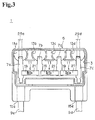
- a known by-pass diode 100 comprises: a rectifier laminate 101 essentially formed by laminating, from bottom to top, a cathode electrode 101a, an n-type domain layer 101b, a p-type domain layer 101c, and an anode electrode 101d, a base lead plate 103, and a top lead plate 105.
- the base lead plate 103 has a rectangular form, one end portion of which is connected to the cathode electrode 101a at the bottom of the rectifier laminate 101 by soldering.
- the top lead plate 105 comprises a rectangular portion 105a and a head portion 105b which is salient from one side end of the rectangular portion and connected to the anode electrode 101d at the top of the rectifier laminate 101 by soldering. Further, the top lead plate 105 and the base lead plate 103 are arranged parallel to each other, but extend along mutually opposite directions from the rectifier laminate 101 (cf. Fig. 2).
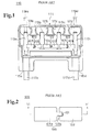
- the above by-pass diode is incorporated into a terminal housing for solar battery modules 110 as shown in Fig.1.
- a housing 111 made of e.g. a synthetic resin comprising a base and sidewalls, the top being left open.
- the base carries, in parallel, e.g. four lead-frame receiver terminals 113a, 113b, 113c and 113d.
- a plurality of by-pass diodes 100 are intercalated between the lead-frame receiver terminals 113a to 113d, such the base lead plate 103 and top lead plate 105 of each by-pass diode are connected respectively to the adjacent lead-frame receiver terminal 113a, 113b, 113c or 113d and soldered thereto.
- the receiver terminals 113a and 113d located at both ends of the housing 111 are respectively connected, by clamping, to corresponding module-linking cables 117a and 117d, which are led into the housing 111 from outside through two fitting holes 115a and 115d formed in a sidewall of the housing 111.
- the base of the housing 111 is further provided with path holes 121a, 121b, 121c and 121d, respectively formed adjacent to the corresponding lead-frame receiver terminals 113a to 113d.
- the housing 111 is then fitted to a solar battery module (not shown in figures), from which are led out a positive-electrode lead frame 119a and a negative-electrode lead frame 119d.
- the positive- and negative-electrode lead frames 119a and 119d are led into the housing 111 through e.g. respective ones of the path holes 121a and 121d and connected to the lead-frame receiver terminals 113a and 113d.
- the housing 111 is then filled with silicone (not shown in figures).
- the by-pass diodes 100 are placed in a housing 111 made of e.g. synthetic resin and embedded therein with e.g. silicone.
- the housing 111 and silicone swell and shrink repeatedly, each time they are used under severe conditions caused e.g. by steep temperature changes. Repeated swelling and shrinking imparts excessive stresses to the portions of the by-pass diodes 100 linking the base and top lead plates 103 and 105 to the rectifier laminate 101. The link portions can then become detached or the rectifier laminate can be become delaminated, thereby causing electrical break.
- An object of the present invention is therefore to provide stress-resistant by-pass rectifier elements, which may be used in a terminal housing for solar battery modules.
- the portions thereof linking the lead plates to the rectifier laminate cannot be delaminated or exfoliated, even when the elements are used under severe climatic conditions repeatedly.
- Another object of the invention is to provide a connector housing for solar battery modules incorporating the above by-pass rectifier element.
- a by-pass rectifier element comprising a rectifier laminate having the form of a chip with first and second faces.
- the by-pass rectifier element further comprises a first lead plate and a second lead plate, each having a longitudinal extension with an end portion, the end portions being arranged respectively on the first face and second face of the rectifier laminate.
- the first lead plate and the second lead plate extend in parallel along opposite directions, respectively from the first face and second face of the rectifier laminate.
- the first lead plate is thinner than the second lead plate.
- the first lead plate comprises a zone adjacent to the end portion, and the zone is provided with slits notched alternately in the direction perpendicular to the longitudinal extension along which the first lead plate extends.
- At least one of the first and second lead plates comprises a rectangular body portion including short sides and long sides, and the end portion of the at least one of the first and second lead plates is formed into a head portion protruding from one of the short sides of the rectangular body.
- the head portion may comprise a neck portion which is constricted width-wise with respect to the head portion.
- the short side of the rectangular body portion may be grooved at both sides of the neck portion along the long side of the rectangular body.
- the invention also relates to a by-pass rectifier element comprising a rectifier laminate having the form of a chip with first and second faces.
- the by-pass rectifier element further comprises a first lead strip and a second lead strip, each having an end portion respectively arranged on the first face and second face of the rectifier laminate.
- the first lead strip and the second lead strip extend in parallel along opposite directions, respectively from the first face and second face of the rectifier laminate.
- At least one of the first and second lead strips then comprises an elongated rectangular body portion including short sides and long sides.
- the end portion of the at least one of the first and second lead strips is formed into a head portion protruding from one of the short side of the elongated rectangular body, and the elongated rectangular body has a width narrower than that of the head portion and extends therefrom.
- the first lead strip is thinner than the second lead strip.
- the invention further concerns a terminal housing incorporating a by-pass rectifier element for solar battery modules as defined above, and further comprising:
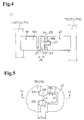
- the terminal housing device for solar battery modules according to a first embodiment of the invention is described with reference to Figs.3 to 6.
- the terminal housing device for solar battery modules 1 (or terminal housing 1) is in the form of a container 5 having e.g. a rectangular base and sidewalls, its top face being open.
- the container 5 is formed of e.g. a synthetic resin and has a container enclosure 3.
- the container enclosure 3 mainly includes e.g. four lead-frame receiver terminals 7a, 7b, 7c and 7d, a pair of module-linking cables 9a and 9b connecting to a power source, and three by-pass rectifier elements 11, e.g. by-pass diodes.
- the rectangular base of the container 5 provides lead-frame path holes 13a, 13b, 13c and 13d along one of the long sides of the container's rectangular base.
- the sidewall rising from the other long side of the container's rectangular base is provided with module-linking cable fitting holes 15a and 15d (or cable fit holes) each having a cylindrical form.
- the cable fit holes 15a and 15d are placed at positions opposing the lead-frame path holes 13a and 13d.
- the lead-frame receiver terminals 7a, 7b, 7c and 7d are respectively placed adjacent the corresponding lead-frame path holes 13a, 13b, 13c and 13d on the rectangular base of the container 5. These lead-frame receiver terminals 7a, 7b, 7c and 7d are held by pinching e.g. by a pair of hooks (not shown in figures) provided on the rectangular base of the container 5.
- a first end of each of the module-linking cables 9a and 9d is led out from the container 5, whilst a second end thereof is led into the container 5 through the corresponding cable fit holes 15a and 15d and electrically connected to the lead-frame receiver terminals 7a and 7b by clamping.
- each group of first and second lead plates 19 and 21 (ut infra) is placed between the corresponding lead-frame receiver terminals 7a, 7b, 7c and 7d, and is electrically connected thereto by e.g. soldering.
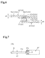
- each by-pass diode 11 comprises: a rectifier laminate 17 in the form of a substantially square-shaped chip, viewed from the top or bottom thereof; a first lead plate 19, placed e.g. on the top side of the rectifier laminate 17; and a second lead plate 21, placed e.g. on the bottom side of the rectifier laminate 17, each plate being made of conductive material e.g. copper, having a substantially rectangular shape, and extending in parallel along opposite directions to each other.
- conductive material e.g. copper
- Each by-rectifier laminate 17 is composed by laminating, from bottom to top, e.g. a cathode electrode 17a, n-type domain material 17b, p-type domain material 17c and an anode electrode 17d, so as to yield a substantially trapezoidal shape.
- the n-type domain material and the p-type domain material form a n-p contact plane therebetween and a corresponding side face surrounding this plane.
- the side face surrounding the contact plane is coated with glass material 17e and is thus passivated.
- the anode electrode 17d is electrically connected, by e.g. soldering, to a longitudinal end portion of the first lead plate 19 from below, whereas the cathode electrode 17a is electrically connected, by e.g. soldering, to a longitudinal end portion of the second lead plate 21 from above.
- soldering (connecting) points are preferably set at the middle along the width of the longitudinal end portions on the first and second lead plates 19 and 21.
- the first lead plate 19 comprises a substantially rectangular body portion 19a, and a head portion 19b which is formed into a substantially rectangular shape having about the same width d1 as that of the top face of the rectifier laminate 17.
- the head portion 19b protrudes horizontally from the longitudinal end portion of the rectangular body portion 19a.
- the bottom face of the head portion 19b is thus connected to the top face of the rectifier laminate 17, i.e. the anode electrode 17d.
- both sides of the head portion 19b are narrowed so as to form a neck portion 23.
- the by-pass diode 11 can thus be flexed easily via the neck portion 23.
- This flexing deformation of the neck portion 23 absorbs the stress exerted on the portion connecting the rectifier laminate 17 to the first and second lead plates 19 and 21, and prevent exfoliation or delamination of this connecting portion.
- the width d2 of the neck portion 23 is preferably made sufficiently narrow.
- the neck portion 23 may have a width d2 of about 0.7 mm.
- the shoulder portions, linking the neck portion 23 to the longitudinal end portion of the rectangular body portion 19a, may be notched into e.g. an arc-shaped recess 25. Then, the length L of the neck portion 23 is effectively increased by the depth of this recess, so that the neck portion 23 becomes further flexible. The protection of the portion connecting the rectifier laminate 17 to the first and second lead plates 19 and 21 is thus further reinforced, and its laminated structure is prevented from becoming exfoliated or delaminated.
- the effective length L of the neck portion 23 is designed preferably to be as great as possible. In the present embodiment, the effective length L of the neck portion 23 is set to be at least 1.0 mm.
- the thickness d3 of the first lead plate 19 is be made thinner than the thickness d4 of the second lead plate 21.
- the first lead late 19 as a whole is rendered further flexible inside the by-pass diode 11, and can absorb the stress imparted to the above-mentioned connecting portion, thereby preventing the exfoliation or delamination of this connecting portion.
- thicknesses d3 and d4a are substantially different, better results can be expected: for instance, d3 and d4 may be set at about 0.1 mm and about 0.2 mm, respectively, to obtain a satisfactory result.
- the rectangular body portion 19a of the relatively thinner first lead plate 19 comprises a zone adjacent the head portion 19b, where a series of slits 27 are cut inwardly at a right angle, alternately from each longitudinal rim of the rectangular body portion 19a.
- the by-pass diode 11 is thus rendered more flexible and bendable by the above slit zone. Accordingly, the flexing deformation of this slit zone further relieves the stress exerted on the portion connecting the rectifier laminate 17 to the first and second lead plates 19 and 21, and prevents the exfoliation of the head portion 19b and the rectifier laminate 17.
- the slit zone is placed near the head portion 19b, and the slits 27 are cut to have a width d5 as narrow as possible.
- the width d5 may be about 0.7 mm.
- the by-pass diode 11 thus prepared is placed between the lead-frame receiver terminal 7a, 7b, 7c or 7d, so that the rectifying direction is arranged in line, and each group consisting of the first lead plate 19 and the second lead plate 21 is electrically connected to the corresponding lead-frame receiver terminals 7a, 7b, 7c and 7d.
- the container 5 is then fitted to a solar battery module (not shown in figures).
- the lead frames 29a and 29b of the respective positive and negative electrodes extending from the above module are drawn into the container 5 through e.g. the frame fitting holes 13a and 13d placed near the lead-frame receiver terminals 7a and 7d, so that the latter, placed at both ends of the container 5, are electrically connected.
- the container 5 is then filled with silicone.
- the first lead plate 19 of the by-pass diode 11 includes a head portion 19b, the root of which is formed into a neck portion 23.
- the first lead plate 19 (thickness d3) is thinner than the second lead plate 21 (thickness d4). That zone of the rectangular body portion 19a in the thinner first lead plate 19, which is adjacent the head portion 19b, is notched into slits 27.
- the first lead plate 19 is thus made flexible and easily bendable. As a result, when the first lead plate 19 is flexed, the resulting flexing deformation can absorb the stress exerted on the portion connecting the rectifier laminate 17 to the first and second lead plates 19 and 21.
- the by-pass diodes 11 wired therein may be subjected to the swelling and shrinking of the resin-made container 5 and the silicone contained in the latter.
- its link portions between the rectifier laminate 17 and the first and second lead plates 19 and 21 may be placed under severe stress. Nonetheless, the link portions of the by-pass diode 11 configured as above can resist to such forces.
- the link portions and the rectifier laminate 17 are thus prevented from detachment or degradation, and the risk of a subsequent electrical cut can be avoided.
- the chip size of the rectifier laminate is small (small soldered area), the above connecting portion can be efficiently protected from detachment.
- the first lead plate 19 of the by-pass diode 11 is placed at the top side of the rectifier laminate 17 and comprises a rectangular body portion 19a, a head portion 19b salient therefrom, and/or a neck portion 23 formed near the head portion 19b.
- the second lead plate 21 is then placed at the bottom side of the rectifier laminate 17 and formed into a rectangular shape.
- both lead plates 19 and 21 may be provided with corresponding rectangular body portions 19a, head portions 19b and/or neck portions 23.
- Such alternative embodiments (second embodiments) can yield the same results as the first embodiment.
- the first lead plate 19 is made thinner than the second lead plate 21 (d3 ⁇ d4), and the former 19 is further provided with slits 27, a head portion 19b and a narrowed neck portion 23. Consequently, the first lead plate 19 is more flexible and bendable than the second lead plate 21. As a result, the stress exerted on the link portions connecting the upper lead plate 19 to the rectifier element body 17 can be neutralized, and the above link portions are efficiently prevented from exfoliation.
- the second lead plate 21 may be made thinner than the first lead plate 19, and the former 21 may be further provided with slits 27, a head portion 19b and/or a neck portion 23.
- Fig.7 shows a variant by-pass diode 11A (third embodiment), which may be used instead of the by-pass diode 11 according to the first and second embodiments.
- the first lead plate 19 is replaced by a first lead strip 31 comprising a strip body portion 31a and a head portion 31b having width d6, and the second lead plate 21 is replaced by a second lead strip 21'.
- the head portion 31b has a size about the same as that of the top surface of the rectifier laminate 17 placed underneath.
- the strip body portion 31a has an elongated rectangular shape with width d7 that is narrower than d6.
- the strip body portion 3 1a is then extended from one end of the head portion 31b.
- the by-pass diode 11A can be easily flexed or bent.
- the stress exerted on the link portions between the rectifier laminate 17 and the lead strips 21 and 31 can thus be absorbed by the flexing deformation of the strip body portion 31a.
- the above link portions, and subsequently the rectifier laminate 17, can thus be prevented efficiently from exfoliation.
- a pair of lead plates are arranged respectively on the top face and the bottom face of the rectifier laminate, one of the lead plates being made thinner than the other.
- the by-pass rectifier element is rendered flexible and bendable, by virtue of the thinner-shaped lead plate.
- the stress exerted on the link portions between the rectifier laminate and the lead plates is absorbed by the flexing deformation of the entire lead plate having a thinner shape.
- the link portions are thus prevented from exfoliation (delamination).
- the thinner lead plate is provided with slits in proximity of the head portion connecting to the rectifier laminate, the slits being notched deeply width-wise, alternately from each longitudinal side of the rectangular body portion.
- the by-pass rectifier element is thus made flexible and bendable in an area near the position where the rectifier laminate is connected.
- the flexing deformation of this area neutralizes the stress exerted on the link portions between the rectifier laminate and the lead plate, and exfoliation of the these portions is efficiently prevented.
- At least one of the lead plates comprises a rectangular body portion, and a head portion protruding from a short side of the rectangular body portion, the head portion comprising a constricted neck portion.
- the by-pass rectifier element is likewise rendered flexible and bendable through the above neck portion.
- the flexing deformation of the neck portion absorbs the stress exerted on the link portion between the rectifier laminate and the lead plate. Hence, the anti-exfoliation effect for the link portions is improved.
- a pair of lead plates are arranged respectively on the top face and the bottom face of the rectifier laminate, and at least one of the lead plates comprises a rectangular body portion, and a head portion protruding from a short side of the rectangular body portion and connecting to the rectifier laminate, the head portion comprising a constricted neck portion.
- the rectangular body portion further comprises shoulder portions at the base of the neck portion, and these shoulder portions are grooved into recesses.
- the neck portions are further lengthened, and the by-pass rectifier element is rendered more flexible and bendable through the lengthened neck portion.
- the flexing deformation of the neck portion thus allows to absorb the stress formed on the link portions between the rectifier laminate and the lead plate, and the link portion is prevented from exfoliation.
- a pair of lead strips are respectively arranged on the top face and the bottom face of the rectifier laminate, and at least one of the lead strips comprises a head portion connecting to the rectifier laminate, and a strip body portion.
- the latter has a width narrower than that of the head portion, and extends from a side rim of the latter.
- the by-pass rectifier element is made flexible and bendable through the narrow strip body portion.
- the stress imparted on the portions linking the rectifier laminate to the lead strips can be absorbed by the flexing deformation of the strip body portion, and the link portions are protected from exfoliation.
- the terminal housing device incorporates a by-pass rectifier element for solar battery modules as defined above.
- the terminal housing device comprises a container formed of e.g. a synthetic resin.
- a container formed of e.g. a synthetic resin.
- Such a container may be filled with e.g. silicone. Accordingly, when the terminal housing device is repeatedly subjected to severe conditions, e.g. to drastically varying temperature environments, the resin container and silicone may swell and shrink. However, even under such conditions, the link portion incorporated in the by-pass diode is prevented from exfoliation and subsequent electrical cut. The terminal housing device of the invention is thus protected by the stress-easing configuration of the above by-pass diode.
Landscapes
- Photovoltaic Devices (AREA)
Applications Claiming Priority (2)
| Application Number | Priority Date | Filing Date | Title |
|---|---|---|---|
| JP2001048208 | 2001-02-23 | ||
| JP2001048208A JP2002252356A (ja) | 2001-02-23 | 2001-02-23 | バイパス用整流素子及びこのバイパス用整流素子を用いた太陽電池モジュール用の端子ボックス装置 |
Publications (1)
| Publication Number | Publication Date |
|---|---|
| EP1237186A2 true EP1237186A2 (de) | 2002-09-04 |
Family
ID=18909516
Family Applications (1)
| Application Number | Title | Priority Date | Filing Date |
|---|---|---|---|
| EP02290408A Withdrawn EP1237186A2 (de) | 2001-02-23 | 2002-02-20 | Überbrückungsdiode und Anschlussgehäuse für Solarzellenmodule mit dieser Diode |
Country Status (3)
| Country | Link |
|---|---|
| US (1) | US6696636B2 (de) |
| EP (1) | EP1237186A2 (de) |
| JP (1) | JP2002252356A (de) |
Cited By (4)
| Publication number | Priority date | Publication date | Assignee | Title |
|---|---|---|---|---|
| EP2475014A3 (de) * | 2011-01-11 | 2013-11-20 | Conergy AG | Photovoltaikmodul mit einlaminierter Bypassdiode |
| EP2345072A4 (de) * | 2008-11-04 | 2014-10-22 | Miasole | Kombinierte dioden-elektrodenanordnung mit dehnungsanschluss |
| US9018513B2 (en) | 2008-05-15 | 2015-04-28 | Apollo Precision (Kunming) Yuanhong Limited | Solar-cell module with in-laminate diodes and external-connection mechanisms mounted to respective edge regions |
| US9059351B2 (en) | 2008-11-04 | 2015-06-16 | Apollo Precision (Fujian) Limited | Integrated diode assemblies for photovoltaic modules |
Families Citing this family (22)
| Publication number | Priority date | Publication date | Assignee | Title |
|---|---|---|---|---|
| US6803514B2 (en) * | 2001-03-23 | 2004-10-12 | Canon Kabushiki Kaisha | Mounting structure and mounting method of a photovoltaic element, mounting substrate for mounting a semiconductor element thereon and method for mounting a semiconductor element on said mounting substrate |
| JP3580313B2 (ja) * | 2003-01-21 | 2004-10-20 | 住友電装株式会社 | 太陽電池モジュール用端子ボックス装置及びその製造方法 |
| JP3580306B2 (ja) * | 2003-01-08 | 2004-10-20 | 住友電装株式会社 | 太陽電池モジュール用端子ボックス装置 |
| DE102004001011B4 (de) | 2003-01-08 | 2010-04-15 | Sumitomo Wiring Systems, Ltd., Yokkaichi | Anschlusskastenvorrichtung für ein Solarzellenmodul und ein Verbindungsverfahren für eine Anschlusskastenvorrichtung |
| JP2005310888A (ja) * | 2004-04-19 | 2005-11-04 | Sumitomo Wiring Syst Ltd | 太陽電池モジュール用端子ボックス及び整流素子ユニット |
| JP3904114B2 (ja) * | 2004-04-23 | 2007-04-11 | 住友電装株式会社 | 太陽電池モジュール用端子ボックスの製造方法 |
| WO2005112133A1 (ja) | 2004-05-19 | 2005-11-24 | Angel Co., Ltd. | 太陽電池用リード端子付ダイオード |
| USD512695S1 (en) * | 2004-06-28 | 2005-12-13 | Angel Co., Ltd. | Diode with lead terminals |
| USD512969S1 (en) * | 2004-06-28 | 2005-12-20 | Angel Co., Ltd. | Twin and parallel diode with lead terminals |
| JP2006179685A (ja) * | 2004-12-22 | 2006-07-06 | Sumitomo Wiring Syst Ltd | 太陽電池モジュール用端子ボックス |
| USD513238S1 (en) * | 2004-12-28 | 2005-12-27 | Angel Co., Ltd. | Diode with lead terminals |
| USD515518S1 (en) * | 2004-12-28 | 2006-02-21 | Angel Co., Ltd. | Twin and parallel diode with lead terminals |
| USD512030S1 (en) * | 2004-12-28 | 2005-11-29 | Angel Co., Ltd. | Twin and parallel diode with lead terminals |
| JP2007036036A (ja) * | 2005-07-28 | 2007-02-08 | Sumitomo Wiring Syst Ltd | 太陽電池モジュール用端子ボックス |
| JP3852710B1 (ja) * | 2005-11-01 | 2006-12-06 | 住友電装株式会社 | 太陽電池モジュール用端子ボックス |
| JP3852711B1 (ja) * | 2005-11-09 | 2006-12-06 | 住友電装株式会社 | 太陽電池モジュール用端子ボックス |
| US20080302031A1 (en) * | 2007-06-05 | 2008-12-11 | Solar Roofing Systems, Inc., | Integrated solar roofing tile connection system |
| CN103390665A (zh) * | 2012-05-07 | 2013-11-13 | 苏州快可光伏电子股份有限公司 | 接线盒 |
| CN103066144B (zh) * | 2012-12-25 | 2015-06-10 | 英利能源(中国)有限公司 | 一种太阳能电池组件及其新的引线方式 |
| CN108566159B (zh) * | 2017-03-10 | 2019-07-26 | 江苏通灵电器股份有限公司 | 太阳能发电组件用芯片低压封装式接线盒的快速加工方法 |
| US10490682B2 (en) | 2018-03-14 | 2019-11-26 | National Mechanical Group Corp. | Frame-less encapsulated photo-voltaic solar panel supporting solar cell modules encapsulated within multiple layers of optically-transparent epoxy-resin materials |
| CN113451234B (zh) * | 2021-05-14 | 2022-10-28 | 上海维攀微电子有限公司 | 一种贴片tvs二极管 |
Family Cites Families (11)
| Publication number | Priority date | Publication date | Assignee | Title |
|---|---|---|---|---|
| JPS5461887A (en) | 1977-10-26 | 1979-05-18 | Sharp Corp | Solar battery device |
| US4577051A (en) * | 1984-09-28 | 1986-03-18 | The Standard Oil Company | Bypass diode assembly for photovoltaic modules |
| JPH0771902B2 (ja) | 1989-06-21 | 1995-08-02 | 富士通テン株式会社 | モータ式定速走行装置 |
| JP2912496B2 (ja) * | 1991-09-30 | 1999-06-28 | シャープ株式会社 | 太陽電池モジュール |
| US5391235A (en) * | 1992-03-31 | 1995-02-21 | Canon Kabushiki Kaisha | Solar cell module and method of manufacturing the same |
| JP2855299B2 (ja) | 1992-04-15 | 1999-02-10 | キヤノン株式会社 | 太陽電池モジュール |
| US5616185A (en) * | 1995-10-10 | 1997-04-01 | Hughes Aircraft Company | Solar cell with integrated bypass diode and method |
| JP3658160B2 (ja) * | 1997-11-17 | 2005-06-08 | キヤノン株式会社 | モールドレス半導体装置 |
| US6103970A (en) * | 1998-08-20 | 2000-08-15 | Tecstar Power Systems, Inc. | Solar cell having a front-mounted bypass diode |
| JP2000196128A (ja) * | 1998-12-25 | 2000-07-14 | Canon Inc | 光起電力素子モジュ―ルおよび太陽電池モジュ―ル、並びに太陽電池モジュ―ルと一体構造の建材 |
| JP2000277785A (ja) * | 1999-03-29 | 2000-10-06 | Matsushita Electronics Industry Corp | 太陽電池モジュール用バイパスダイオード |
-
2001
- 2001-02-23 JP JP2001048208A patent/JP2002252356A/ja not_active Abandoned
-
2002
- 2002-02-20 EP EP02290408A patent/EP1237186A2/de not_active Withdrawn
- 2002-02-22 US US10/079,548 patent/US6696636B2/en not_active Expired - Fee Related
Cited By (4)
| Publication number | Priority date | Publication date | Assignee | Title |
|---|---|---|---|---|
| US9018513B2 (en) | 2008-05-15 | 2015-04-28 | Apollo Precision (Kunming) Yuanhong Limited | Solar-cell module with in-laminate diodes and external-connection mechanisms mounted to respective edge regions |
| EP2345072A4 (de) * | 2008-11-04 | 2014-10-22 | Miasole | Kombinierte dioden-elektrodenanordnung mit dehnungsanschluss |
| US9059351B2 (en) | 2008-11-04 | 2015-06-16 | Apollo Precision (Fujian) Limited | Integrated diode assemblies for photovoltaic modules |
| EP2475014A3 (de) * | 2011-01-11 | 2013-11-20 | Conergy AG | Photovoltaikmodul mit einlaminierter Bypassdiode |
Also Published As
| Publication number | Publication date |
|---|---|
| JP2002252356A (ja) | 2002-09-06 |
| US20020117200A1 (en) | 2002-08-29 |
| US6696636B2 (en) | 2004-02-24 |
Similar Documents
| Publication | Publication Date | Title |
|---|---|---|
| EP1237186A2 (de) | Überbrückungsdiode und Anschlussgehäuse für Solarzellenmodule mit dieser Diode | |
| US6655987B2 (en) | Terminal box apparatus for solar cell module | |
| CN101345266B (zh) | 太阳能电池模块 | |
| US20110073154A1 (en) | Solar cell module | |
| US20090078301A1 (en) | Solar cell module | |
| US7920385B2 (en) | Terminal box for solar cell module | |
| US8969708B2 (en) | Solar cell module | |
| CN100557825C (zh) | 用于太阳能电池模块的接线盒 | |
| EP3984082A1 (de) | Batterieanordnung und elektrochemische vorrichtung | |
| EP2234167A2 (de) | Solarzelle und Solarzellenmodul | |
| SI1547158T1 (sl) | Elektroda za fotovoltaicne celice, fotovoltaicna celica in fotovoltaicni modul | |
| JP2013542614A (ja) | 太陽電池モジュール及びその製造方法 | |
| CN1728417A (zh) | 用于二次电池的二次保护元件 | |
| US8547685B2 (en) | Terminal box for solar cell module | |
| EP0481094A4 (de) | ||
| US20130247956A1 (en) | Solar cell module | |
| EP3179627B1 (de) | Photovoltaikanschlusskasten | |
| US9306081B2 (en) | Solar cell module | |
| CN110931586A (zh) | 焊带、柔性太阳能电池组件 | |
| US9954484B2 (en) | Solar battery module | |
| EP2450968A2 (de) | Photovoltaikvorrichtung | |
| KR102734380B1 (ko) | 선형 전지가 교차 구조물 형태로 형성된 플렉서블 이차전지 | |
| JP2011029500A (ja) | 太陽電池用素子装置 | |
| KR20200089560A (ko) | 데드존을 최소화한 광 투과형 플렉시블 박막 태양전지 모듈 | |
| CN208315574U (zh) | 焊带、柔性太阳能电池组件 |
Legal Events
| Date | Code | Title | Description |
|---|---|---|---|
| PUAI | Public reference made under article 153(3) epc to a published international application that has entered the european phase |
Free format text: ORIGINAL CODE: 0009012 |
|
| AK | Designated contracting states |
Kind code of ref document: A2 Designated state(s): AT BE CH CY DE DK ES FI FR GB GR IE IT LI LU MC NL PT SE TR |
|
| AX | Request for extension of the european patent |
Free format text: AL;LT;LV;MK;RO;SI |
|
| STAA | Information on the status of an ep patent application or granted ep patent |
Free format text: STATUS: THE APPLICATION HAS BEEN WITHDRAWN |
|
| 18W | Application withdrawn |
Effective date: 20070820 |