EP1237182A2 - Succession de couches diélectriques pour réduire la consommation de nitrure - Google Patents
Succession de couches diélectriques pour réduire la consommation de nitrure Download PDFInfo
- Publication number
- EP1237182A2 EP1237182A2 EP02250813A EP02250813A EP1237182A2 EP 1237182 A2 EP1237182 A2 EP 1237182A2 EP 02250813 A EP02250813 A EP 02250813A EP 02250813 A EP02250813 A EP 02250813A EP 1237182 A2 EP1237182 A2 EP 1237182A2
- Authority
- EP
- European Patent Office
- Prior art keywords
- layer
- aggregate
- substrate
- film
- dielectric layer
- Prior art date
- Legal status (The legal status is an assumption and is not a legal conclusion. Google has not performed a legal analysis and makes no representation as to the accuracy of the status listed.)
- Withdrawn
Links
Images
Classifications
-
- H—ELECTRICITY
- H10—SEMICONDUCTOR DEVICES; ELECTRIC SOLID-STATE DEVICES NOT OTHERWISE PROVIDED FOR
- H10P—GENERIC PROCESSES OR APPARATUS FOR THE MANUFACTURE OR TREATMENT OF DEVICES COVERED BY CLASS H10
- H10P14/00—Formation of materials, e.g. in the shape of layers or pillars
- H10P14/60—Formation of materials, e.g. in the shape of layers or pillars of insulating materials
- H10P14/69—Inorganic materials
- H10P14/692—Inorganic materials composed of oxides, glassy oxides or oxide-based glasses
- H10P14/6921—Inorganic materials composed of oxides, glassy oxides or oxide-based glasses containing silicon
- H10P14/6922—Inorganic materials composed of oxides, glassy oxides or oxide-based glasses containing silicon the material containing Si, O and at least one of H, N, C, F or other non-metal elements, e.g. SiOC, SiOC:H or SiONC
- H10P14/6923—Inorganic materials composed of oxides, glassy oxides or oxide-based glasses containing silicon the material containing Si, O and at least one of H, N, C, F or other non-metal elements, e.g. SiOC, SiOC:H or SiONC the material being boron or phosphorus doped silicon oxides, e.g. BPSG, BSG or PSG
-
- H—ELECTRICITY
- H10—SEMICONDUCTOR DEVICES; ELECTRIC SOLID-STATE DEVICES NOT OTHERWISE PROVIDED FOR
- H10P—GENERIC PROCESSES OR APPARATUS FOR THE MANUFACTURE OR TREATMENT OF DEVICES COVERED BY CLASS H10
- H10P14/00—Formation of materials, e.g. in the shape of layers or pillars
- H10P14/60—Formation of materials, e.g. in the shape of layers or pillars of insulating materials
- H10P14/63—Formation of materials, e.g. in the shape of layers or pillars of insulating materials characterised by the formation processes
- H10P14/6326—Deposition processes
- H10P14/6328—Deposition from the gas or vapour phase
- H10P14/6334—Deposition from the gas or vapour phase using decomposition or reaction of gaseous or vapour phase compounds, i.e. chemical vapour deposition
-
- H—ELECTRICITY
- H10—SEMICONDUCTOR DEVICES; ELECTRIC SOLID-STATE DEVICES NOT OTHERWISE PROVIDED FOR
- H10P—GENERIC PROCESSES OR APPARATUS FOR THE MANUFACTURE OR TREATMENT OF DEVICES COVERED BY CLASS H10
- H10P14/00—Formation of materials, e.g. in the shape of layers or pillars
- H10P14/60—Formation of materials, e.g. in the shape of layers or pillars of insulating materials
- H10P14/65—Formation of materials, e.g. in the shape of layers or pillars of insulating materials characterised by treatments performed before or after the formation of the materials
- H10P14/6502—Formation of materials, e.g. in the shape of layers or pillars of insulating materials characterised by treatments performed before or after the formation of the materials of treatments performed before formation of the materials
- H10P14/6506—Formation of intermediate materials
-
- H—ELECTRICITY
- H10—SEMICONDUCTOR DEVICES; ELECTRIC SOLID-STATE DEVICES NOT OTHERWISE PROVIDED FOR
- H10P—GENERIC PROCESSES OR APPARATUS FOR THE MANUFACTURE OR TREATMENT OF DEVICES COVERED BY CLASS H10
- H10P95/00—Generic processes or apparatus for manufacture or treatments not covered by the other groups of this subclass
- H10P95/06—Planarisation of inorganic insulating materials
-
- H—ELECTRICITY
- H10—SEMICONDUCTOR DEVICES; ELECTRIC SOLID-STATE DEVICES NOT OTHERWISE PROVIDED FOR
- H10W—GENERIC PACKAGES, INTERCONNECTIONS, CONNECTORS OR OTHER CONSTRUCTIONAL DETAILS OF DEVICES COVERED BY CLASS H10
- H10W20/00—Interconnections in chips, wafers or substrates
- H10W20/40—Interconnections external to wafers or substrates, e.g. back-end-of-line [BEOL] metallisations or vias connecting to gate electrodes
- H10W20/45—Interconnections external to wafers or substrates, e.g. back-end-of-line [BEOL] metallisations or vias connecting to gate electrodes characterised by their insulating parts
- H10W20/48—Insulating materials thereof
Definitions
- the invention relates to passivation or dielectric layers used in, for example, circuit structures.
- Dielectric layers or films are used to electrically isolate one device from another in a circuit structure and one level of conductor from another in multi-level interconnect systems such as found in many integrated circuit structures .
- a microprocessor may have five or more levels of interconnect over a substrate such as a semiconductor substrate.
- PMD pre-metal dielectric
- the substrate or device base e.g., the substrate containing active devices therein/thereon
- the first interconnect level e.g., Metal 1
- PMD layers or films can typically be deposited (and densified if necessary) at a higher temperature than is possible for intermetal dielectric layers.
- PMD films can be flowed and reflowed at temperatures in excess of 700°C to promote gap fill.
- the PMD layer or film isolates devices in an integrated circuit structure in two ways. It isolates devices electrically from interconnect layers, and it isolates devices physically from contamination sources such as mobile ions (e.g., from post-processing and handling). Mobile ions such as sodium and potassium tend to degrade essential device characteristics such as the threshold voltage of a transistor device.
- one criteria for filling a gap in a PMD process is 0.1 microns ( ⁇ m) with a 5 to 1 aspect ratio.
- BPSG Borophosphosilicate glass
- SiO 2 Borophosphosilicate glass
- BPSG typically contains about two to six weight percent each of boron and phosphorous.
- BPSG is typically deposited using thermal chemical vapor deposition (CVD) at 400 to 700°C, and then annealed (reflowed) at 700 to 1000°C.
- CVD thermal chemical vapor deposition
- the phosphorus in BPSG acts as a gettering agent for any mobile ions that may diffuse toward the devices (e.g., transistors), while the boron provides good gap fill because it tends to soften the layer after the reflow anneal.
- a thin layer of silicon nitride (Si 3 N 4 ) is introduced over the substrate as an initial dielectric layer or film followed by, for example, a BPSG layer or film.
- the silicon nitride also serves in one instance as an etch stop in planarizing a subsequently introduced PMD layer or film, such as a BPSG layer or film.
- gap fill of a PMD layer or film is increasingly important as device densities increase.
- the gap fill properties of a BPSG layer or film is optimized by annealing at more than 800°C.
- the high temperature anneal tends to increase the reflow ability of the BPSG.
- one drawback to the high temperature anneal and reflow process is that the BPSG material tends to consume nitrogen from the underlying silicon nitride layer or film.
- the nitride consumption tends to degrade the insulating properties of the silicon nitride material.
- what is needed is a way to control the nitrogen consumption of nitrogen-containing layers or films in conjunction with a thermal processing in the presence of phosphorous.
- a method includes, over a circuit substrate, forming an aggregate comprising a barrier layer between a first dielectric layer comprising nitrogen and a second dielectric layer comprising phosphorus.
- the method also includes, after forming the aggregate, thermally treating the circuit substrate.
- a suitable introduction point for implementing the method described herein is in a PMD layer or film, wherein the circuit substrate comprises a device base and at least one metal layer and the aggregate is introduced between the device base and the at least one metal layer.
- Suitable barrier layers include dielectric materials, particularly silicates such as borosilicate glass (BSG) or undoped silicate glass (USG).
- BSG borosilicate glass
- USG undoped silicate glass
- a thin film of, for example, BSG or USG between a silicon nitride film and BPSG material tends to reduce the consumption during reflow (thermally annealing) the BPSG.
- the invention in another embodiment, relates to an apparatus.
- the apparatus includes, in one aspect, a circuit substrate and an aggregate comprising a barrier layer between a first dielectric layer comprising nitrogen and a second dielectric layer comprising phosphorus.
- an aggregate as a PMD layer or film comprising a barrier layer of a dielectric material such as BSG or USG disposed between a silicon nitride layer and a BPSG layer as the aggregate of a PMD film.
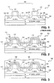
- Figure 1 schematically illustrates a cross-sectional side view of a portion of an integrated circuit substrate including devices formed thereon and therein in accordance with an embodiment of the invention.
- Figure 2 shows the structure of Figure 1 following the introduction of a portion of an aggregate layer or film including a nitrogen-containing dielectric layer and a barrier layer in accordance with an embodiment of the invention.
- Figure 3 shows the structure of Figure 2 following the introduction and planarization of a dielectric film containing phosphorus in accordance with one embodiment of the invention.
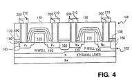
- Figure 4 shows the structure of Figure 3 after the introduction of interconnect structures over the planarized dielectric film.
- An aggregate suitable as a dielectric or passivation layer of an integrated circuit structure is described, as is an embodiment of a method of implementing the aggregate and an apparatus including the aggregate.
- a method including, over a circuit substrate, forming an aggregate comprising a barrier layer between a first dielectric layer comprising nitrogen and a second dielectric layer comprising phosphorus; and, after forming the aggregate, thermally treating the circuit substrate.
- a barrier layer or film that is a dielectric material such as borosilicate glass (BSG) or undoped silicate glass (USG) separating a silicon nitride layer or film from a borophosphosilicate glass (BPSG) layer or film.
- BSG borosilicate glass
- USG undoped silicate glass
- the barrier layer or film reduces or minimizes the nitrogen consumption generally seen between the BPSG layer or film and the silicon nitride layer or film, particularly during thermal reflow.
- an aggregate includes multiple layers or films introduced or formed on a circuit substrate.
- an aggregate as described herein includes or may be referenced as a "layer" as, for example, a PMD layer or intermetal layer is described.
- FIG. 1 schematically shows a cross-sectional side view of a portion of an integrated circuit substrate having devices formed thereon and therein.
- structure 100 includes substrate 102 that is for example a semiconductor substrate including N-type transistor device 105 and P-type transistor device 115.
- Transistor devices 105 and 115 are separated from one other and formed in active device regions defined by shallow trench isolation (STI) structures 150.
- N-type transistor device 105 includes gate electrode 110 formed over the surface of substrate 102 (typically over a gate dielectric) and junction or diffusion regions 130 formed in substrate 102.
- Transistor device 115 includes gate electrode 120 formed over the surface of substrate 102 and junction or diffusion regions 140 formed in substrate 102.
- a PMD layer or film is introduced over the surface of the structure to isolate the individual transistor devices and the interconnect structures that form the electrical connections to the devices.
- the PMD layer should have adequate gap fill to fill gaps, such as gap 160 between the transistor devices.
- Figure 2 shows the structure of Figure 1 after the introduction of a thin film of a nitrogen-containing dielectric material, such as silicon nitride (Si 3 N 4 ), over surface 108 of substrate 102.
- a nitrogen-containing dielectric material such as silicon nitride (Si 3 N 4 )
- nitrogen-containing layer or film 170 is conformably introduced over surface 108 of substrate 102 and over gate electrodes 110 and 120, respectively.
- Nitrogen-containing layer or film 170 serves both as a dielectric or passivation layer as well as an etch stop for forming openings through a subsequently introduced dielectric material as will become clear in the following paragraphs.
- Silicon nitride is generally considered to have a dielectric constant that is too high to make it suitable as a complete PMD layer.
- silicon nitride is introduced such as by chemical vapor deposition (CVD), as a thin film on the order of, for example, about 20 to 200 angstroms to serve a purpose as an etch stop.
- CVD chemical vapor deposition
- Figure 2 also shows the structure of Figure 1 following the conformal introduction of barrier layer or film 180 over nitrogen-containing layer or film 170.
- Barrier layer or film 180 is selected, in one embodiment, as a material that would tend not to consume the nitrogen in nitrogen-containing layer or film 170 during subsequent thermal processing or annealing.
- barrier layer or film 180 is selected to be a material that has properties (e.g., reflow properties) enabling the achievement of suitable gap fill criteria with state of the art device densities.
- Suitable materials for barrier layer or film 180 include, but are not limited to, dielectric materials that do not contain phosphorous. It is believed during reflow or thermal processing that phosphorus consumes nitrogen. By adding a barrier layer or film that is free of phosphorous, the nitrogen consumption during subsequent thermal processing may be controlled.
- Representative materials for barrier layer or film 180 include, but are not limited to, borosilicate glass (BSG) and undoped silicate glass (USG).
- BSG and USG may be introduced as thin films on the order of, in one example, less than 1000 ⁇ m (where the subsequently applied layer or film is BPSG).
- RTP rapid thermal processing
- Figure 3 shows the structure of Figure 2 following the introduction of phosphorous-containing layer or film 190 over the structure.
- phosphorous-containing layer or film 190 is a dielectric material selected for its gap-fill properties, particularly, as here, where the material forms a portion of a PMD layer. The gettering properties of the phosphorous are also desirous.
- One suitable material for phosphorous-containing layer or film 190 is borophosphosilicate glass (BPSG).
- borophosphosilicate glass borophosphosilicate glass
- phosphorous-containing layer or film 190 is conformably deposited to a thickness on the order of, for example, greater than 2000 angstroms for state of the art integrated circuit structures.
- a typical introduction technique is CVD.
- structure 100 may be subjected to thermal processing or annealing following introduction of the PMD layer.
- Annealing or thermal processing temperatures greater than 700°C, such as 830°C in the presence of steam or nitrogen gas in an RTP process for BPSG is suitable.
- barrier layer or film 180 it is also believed, effectively slows the path of phosphorus to nitrogen in nitrogen-containing layer or film 170. By slowing the path, less nitrogen is consumed. In this regard, the insulating properties of nitrogen-containing layer or film 170 will not be diminished due to nitrogen consumption.
- Figures 1-3 show a PMD layer or film that is an aggregate of nitrogen-containing layer or film 170, barrier layer or film 180, and phosphorous-containing layer or film 190. It is to be appreciated that the layers of the aggregate may remain as individual layers or, particularly given the subsequent thermal processing to which the materials may be exposed, combined in an additive or reactive fashion.
- Figure 4 shows the structure of Figure 3 following the planarization of phosphorous-containing layer or film 190 and the formation and filling of vias or openings to diffusion or junction regions of individual transistor devices 105 and 115, respectively.
- the planarization of phosphorous-containing layer or film 190 of BPSG is accomplished through a polish (e.g., a chemical-mechanical polish) as known in the art.
- Vias or openings are formed through phosphorous-containing layer or film 190, barrier layer or film 180 and nitrogen-containing layer or film 170 through etching, with for example, an etch chemistry as known in the art.
- the selection of material for barrier layer or film 180 may be such that a single etch chemistry may be used to form an opening through both phosphorous-containing layer or film 190 and barrier layer or film 180.
- a dry etch may be used.
- the openings or vias may be filled with a conductive material.
- a conductive material One common approach is to introduce a titanium adhesion layer along the sidewalls of the opening or via, followed by a titanium nitride barrier layer also along the sidewalls. The remainder of the opening or via is then filled with tungsten.
- Interconnects 210 of for example, aluminum or copper material (including alloys of aluminum or copper) are then introduced and patterned on surface 195 of PMD layer over the conductive vias or openings. The introduction and patterning of interconnects 210 may be accomplished as known in the art.
- an aggregate suitable as a PMD layer is described.
- the aggregate is described in terms of a PMD layer where a phosphorous-containing dielectric material (e.g., BPSG) is often used in conjunction with a nitrogen-containing material (e.g., Si 3 N 4 ).
- a phosphorous-containing dielectric material e.g., BPSG
- a nitrogen-containing material e.g., Si 3 N 4
- the presence of the barrier layer or film tends to reduce nitrogen consumption generally seen during thermal processing between directly-disposed phosphorous- and nitrogen-containing materials.
- an aggregate such as described may be used in a variety of situations where nitrogen consumption in the presence of phosphorous is a concern.
- Such other applications include, but are not limited to, intermetal dielectric layers or films.
Landscapes
- Internal Circuitry In Semiconductor Integrated Circuit Devices (AREA)
- Formation Of Insulating Films (AREA)
Applications Claiming Priority (2)
| Application Number | Priority Date | Filing Date | Title |
|---|---|---|---|
| US09/789,455 US6514882B2 (en) | 2001-02-19 | 2001-02-19 | Aggregate dielectric layer to reduce nitride consumption |
| US789455 | 2001-02-19 |
Publications (2)
| Publication Number | Publication Date |
|---|---|
| EP1237182A2 true EP1237182A2 (fr) | 2002-09-04 |
| EP1237182A3 EP1237182A3 (fr) | 2002-10-02 |
Family
ID=25147695
Family Applications (1)
| Application Number | Title | Priority Date | Filing Date |
|---|---|---|---|
| EP02250813A Withdrawn EP1237182A3 (fr) | 2001-02-19 | 2002-02-06 | Succession de couches diélectriques pour réduire la consommation de nitrure |
Country Status (6)
| Country | Link |
|---|---|
| US (1) | US6514882B2 (fr) |
| EP (1) | EP1237182A3 (fr) |
| KR (1) | KR20020067990A (fr) |
| CN (1) | CN1372303A (fr) |
| SG (1) | SG97230A1 (fr) |
| TW (1) | TW557540B (fr) |
Families Citing this family (7)
| Publication number | Priority date | Publication date | Assignee | Title |
|---|---|---|---|---|
| US6967143B2 (en) * | 2003-04-30 | 2005-11-22 | Freescale Semiconductor, Inc. | Semiconductor fabrication process with asymmetrical conductive spacers |
| KR100503951B1 (ko) * | 2003-04-30 | 2005-07-26 | 주식회사 하이닉스반도체 | 반도체 소자의 제조 방법 |
| US20060157776A1 (en) * | 2005-01-20 | 2006-07-20 | Cheng-Hung Chang | System and method for contact module processing |
| US20070210421A1 (en) * | 2006-03-13 | 2007-09-13 | Texas Instruments Inc. | Semiconductor device fabricated using a carbon-containing film as a contact etch stop layer |
| US7884030B1 (en) | 2006-04-21 | 2011-02-08 | Advanced Micro Devices, Inc. and Spansion LLC | Gap-filling with uniform properties |
| US8435898B2 (en) * | 2007-04-05 | 2013-05-07 | Freescale Semiconductor, Inc. | First inter-layer dielectric stack for non-volatile memory |
| CN103219235B (zh) * | 2013-04-03 | 2016-10-05 | 无锡华润上华科技有限公司 | 一种改善高压器件晶体管漏电的方法 |
Family Cites Families (9)
| Publication number | Priority date | Publication date | Assignee | Title |
|---|---|---|---|---|
| US4091407A (en) | 1976-11-01 | 1978-05-23 | Rca Corporation | Combination glass/low temperature deposited Siw Nx Hy O.sub.z |
| JPS57199224A (en) | 1981-06-02 | 1982-12-07 | Nec Corp | Semiconductor device |
| US4952524A (en) * | 1989-05-05 | 1990-08-28 | At&T Bell Laboratories | Semiconductor device manufacture including trench formation |
| US5166088A (en) | 1990-07-03 | 1992-11-24 | Sharp Kabushiki Kaisha | Method of manufacturing semiconductor device contact vias in layers comprising silicon nitride and glass |
| JP2672181B2 (ja) * | 1990-07-04 | 1997-11-05 | シャープ株式会社 | 半導体装置の製造方法 |
| JPH07183250A (ja) | 1993-12-24 | 1995-07-21 | Sharp Corp | コンタクト形成方法 |
| JP3105788B2 (ja) * | 1996-07-15 | 2000-11-06 | 日本電気株式会社 | 半導体装置の製造方法 |
| US6063656A (en) | 1997-04-18 | 2000-05-16 | Micron Technology, Inc. | Cell capacitors, memory cells, memory arrays, and method of fabrication |
| KR20000013539A (ko) * | 1998-08-10 | 2000-03-06 | 윤종용 | 열산화를 이용한 게이트 유전막의 형성 방법 |
-
2001
- 2001-02-19 US US09/789,455 patent/US6514882B2/en not_active Expired - Fee Related
-
2002
- 2002-02-06 TW TW091102128A patent/TW557540B/zh not_active IP Right Cessation
- 2002-02-06 EP EP02250813A patent/EP1237182A3/fr not_active Withdrawn
- 2002-02-06 SG SG200200736A patent/SG97230A1/en unknown
- 2002-02-10 CN CN02104751A patent/CN1372303A/zh active Pending
- 2002-02-19 KR KR1020020008703A patent/KR20020067990A/ko not_active Ceased
Also Published As
| Publication number | Publication date |
|---|---|
| CN1372303A (zh) | 2002-10-02 |
| KR20020067990A (ko) | 2002-08-24 |
| TW557540B (en) | 2003-10-11 |
| US20020115302A1 (en) | 2002-08-22 |
| SG97230A1 (en) | 2003-07-18 |
| US6514882B2 (en) | 2003-02-04 |
| EP1237182A3 (fr) | 2002-10-02 |
Similar Documents
| Publication | Publication Date | Title |
|---|---|---|
| KR100564188B1 (ko) | 반도체집적회로장치및그제조방법 | |
| US7088003B2 (en) | Structures and methods for integration of ultralow-k dielectrics with improved reliability | |
| US6348407B1 (en) | Method to improve adhesion of organic dielectrics in dual damascene interconnects | |
| US7816280B2 (en) | Semiconductor device, semiconductor wafer, and methods of producing the same device and wafer | |
| KR100940395B1 (ko) | 반도체 집적 회로 장치 | |
| EP1349207A2 (fr) | Dispositif semiconducteur avec interconnexions en cuivre | |
| US6541861B2 (en) | Semiconductor device manufacturing method including forming step of SOI structure and semiconductor device having SOI structure | |
| US20100096699A1 (en) | Prevention of plasma induced damage arising from etching of crack stop trenches in multi-layered low-k semiconductor devices | |
| JP2010056156A (ja) | 半導体装置およびその製造方法 | |
| US6650017B1 (en) | Electrical wiring of semiconductor device enabling increase in electromigration (EM) lifetime | |
| US6489254B1 (en) | Method of forming pre-metal dielectric film on a semiconductor substrate including first layer of undoped oxide of high ozone:TEOS volume ratio and second layer of low ozone doped BPSG | |
| US6911394B2 (en) | Semiconductor devices and methods of manufacturing such semiconductor devices | |
| US6514882B2 (en) | Aggregate dielectric layer to reduce nitride consumption | |
| US20050140012A1 (en) | Method for forming copper wiring of semiconductor device | |
| KR100783868B1 (ko) | 반도체장치의 제조방법 및 반도체장치 | |
| JPH07297276A (ja) | 半導体集積回路の形成方法 | |
| US6218289B1 (en) | Method for contact anneal in a doped dielectric layer without dopant diffusion problem | |
| KR100596277B1 (ko) | 반도체 소자 및 그의 절연막 형성 방법 | |
| EP1008175A1 (fr) | Couche intermediaire dielectrique coiffee pour polissage chimico-mecanique | |
| KR101029105B1 (ko) | 반도체 소자의 금속배선 및 그 형성방법 | |
| KR20020011475A (ko) | 저유전율 절연막이 포함된 다마신공정법 | |
| KR20050056650A (ko) | 반도체 소자의 층간 절연막 형성 방법 | |
| KR20030069375A (ko) | 실리콘 산화막의 제조 방법 |
Legal Events
| Date | Code | Title | Description |
|---|---|---|---|
| PUAI | Public reference made under article 153(3) epc to a published international application that has entered the european phase |
Free format text: ORIGINAL CODE: 0009012 |
|
| PUAL | Search report despatched |
Free format text: ORIGINAL CODE: 0009013 |
|
| AK | Designated contracting states |
Kind code of ref document: A2 Designated state(s): AT BE CH CY DE DK ES FI FR GB GR IE IT LI LU MC NL PT SE TR |
|
| AX | Request for extension of the european patent |
Free format text: AL;LT;LV;MK;RO;SI |
|
| AK | Designated contracting states |
Kind code of ref document: A3 Designated state(s): AT BE CH CY DE DK ES FI FR GB GR IE IT LI LU MC NL PT SE TR |
|
| AX | Request for extension of the european patent |
Free format text: AL;LT;LV;MK;RO;SI |
|
| RIN1 | Information on inventor provided before grant (corrected) |
Inventor name: MUKAI, KEVIN M. Inventor name: CHANDRAN, SHANKAR |
|
| 17P | Request for examination filed |
Effective date: 20030206 |
|
| 17Q | First examination report despatched |
Effective date: 20030317 |
|
| AKX | Designation fees paid |
Designated state(s): DE FR GB IT NL |
|
| STAA | Information on the status of an ep patent application or granted ep patent |
Free format text: STATUS: THE APPLICATION IS DEEMED TO BE WITHDRAWN |
|
| 18D | Application deemed to be withdrawn |
Effective date: 20030728 |