EP1230668B1 - Plasma processing apparatus for producing uniform process rates - Google Patents
Plasma processing apparatus for producing uniform process rates Download PDFInfo
- Publication number
- EP1230668B1 EP1230668B1 EP00993006A EP00993006A EP1230668B1 EP 1230668 B1 EP1230668 B1 EP 1230668B1 EP 00993006 A EP00993006 A EP 00993006A EP 00993006 A EP00993006 A EP 00993006A EP 1230668 B1 EP1230668 B1 EP 1230668B1
- Authority
- EP
- European Patent Office
- Prior art keywords
- layer
- antenna
- plasma
- turn
- process chamber
- Prior art date
- Legal status (The legal status is an assumption and is not a legal conclusion. Google has not performed a legal analysis and makes no representation as to the accuracy of the status listed.)
- Expired - Lifetime
Links
Images


Classifications
-
- H—ELECTRICITY
- H05—ELECTRIC TECHNIQUES NOT OTHERWISE PROVIDED FOR
- H05H—PLASMA TECHNIQUE; PRODUCTION OF ACCELERATED ELECTRICALLY-CHARGED PARTICLES OR OF NEUTRONS; PRODUCTION OR ACCELERATION OF NEUTRAL MOLECULAR OR ATOMIC BEAMS
- H05H1/00—Generating plasma; Handling plasma
- H05H1/24—Generating plasma
- H05H1/46—Generating plasma using applied electromagnetic fields, e.g. high frequency or microwave energy
-
- H—ELECTRICITY
- H01—ELECTRIC ELEMENTS
- H01J—ELECTRIC DISCHARGE TUBES OR DISCHARGE LAMPS
- H01J37/00—Discharge tubes with provision for introducing objects or material to be exposed to the discharge, e.g. for the purpose of examination or processing thereof
- H01J37/32—Gas-filled discharge tubes
- H01J37/32431—Constructional details of the reactor
- H01J37/32458—Vessel
- H01J37/32467—Material
-
- H—ELECTRICITY
- H01—ELECTRIC ELEMENTS
- H01J—ELECTRIC DISCHARGE TUBES OR DISCHARGE LAMPS
- H01J37/00—Discharge tubes with provision for introducing objects or material to be exposed to the discharge, e.g. for the purpose of examination or processing thereof
- H01J37/32—Gas-filled discharge tubes
- H01J37/32009—Arrangements for generation of plasma specially adapted for examination or treatment of objects, e.g. plasma sources
- H01J37/32082—Radio frequency generated discharge
- H01J37/321—Radio frequency generated discharge the radio frequency energy being inductively coupled to the plasma
Definitions
- the present invention relates to apparatus and methods for processing substrates such as semiconductor substrates for use in IC fabrication or glass panels for use in flat panel display applications. More particularly, the present invention relates to improved plasma processing systems that are capable of processing substrates with a high degree of processing uniformity across the substrate surface.
- Plasma processing systems have been around for some time. Over the years, plasma processing systems utilizing inductively coupled plasma sources, electron cyclotron resonance (ECR) sources, capacitive sources, and the like, have been introduced and employed to various degrees to process semiconductor substrates and glass panels.
- ECR electron cyclotron resonance
- etching steps are typically employed.
- materials are deposited onto a substrate surface (such as the surface of a glass panel or a wafer),
- a substrate surface such as the surface of a glass panel or a wafer
- deposited layers such as various forms of silicon, silicon dioxide, silicon nitride, metals and the like may be formed on the surface of the substrate.
- etching may be employed to selectively remove materials from predefined areas on the substrate surface. For example, etched features such as vias, contacts, or trenches may be formed in the layers of the substrate.
- FIG. 1 illustrates a prior art inductive plasma processing reactor 100 that is used for plasma processing.
- a typical inductive plasma processing reactor includes a chamber 102 with an antenna or inductive coil 104 disposed above a dielectric window 106.
- antenna 104 is operatively coupled to a first RF power source 108.
- a gas port 110 is provided within chamber 102 that is arranged for releasing gaseous source materials, e.g., the etchant source gases, into the RF-induced plasma region between dielectric window 106 and a substrate 112.
- Substrate 112 is introduced into chamber 102 and disposed on a chuck 114, which generally acts as an electrode and is operatively coupled to a second RF power source 116.
- a process gas is input into chamber 102 through gas port 110. Power is then supplied to inductive coil 104 using first RF power source 108. The supplied RF energy couples through the dielectric window 106 and a large electric field is induced inside chamber 102. More specifically, in response to the electric field, a circulating current is induced in chamber 102. The electric field accelerates the small number of electrons present inside the chamber causing them to collide with the gas molecules of the process gas. These collisions result in ionization and initiation of a discharge or plasma 118. As is well known in the art, the neutral gas molecules of the process gas when subjected to these strong electric fields lose electrons, and leave behind positively charged ions. As a result, positively charged ions, negatively charged electrons and neutral gas molecules (and/or atoms) are contained inside the plasma 118. As soon as the creation rate of free electrons exceeds their loss rate, the plasma ignites.
- neutral gas molecules inside the plasma tend to be directed towards the surface of the substrate.
- one of the mechanism contributing to the presence of the neutrals gas molecules at the substrate may be diffusion (i.e., the random movement of molecules inside the chamber).
- a layer of neutral species e.g., neutral gas molecules
- ions tend to accelerate towards the substrate where they, in combination with neutral species, activate the etching reaction.
- etch performance across the substrate e.g., a non-uniform etch rate. That is, one area of the substrate gets etched differently than another area. As a result, it is extremely difficult to control the parameters associated with the integrated circuit, i.e., critical dimensions, aspect ratios, and the like. Additionally, a non-uniform etch rate may lead to device failure in the semiconductor circuit, which typically translates into higher costs for the manufacturer. Moreover, there also exist other issues of concern such as the overall etch rate, etch profile, micro-loading, selectivity, and the like.
- these non-uniform etch rates may be the result of variations in the plasma density across the surface of the substrate, i.e., a plasma that has regions with greater or lesser amounts of reactive species (e.g., positively charged ions). While not wishing to be bound by theory, it is believed that the variations in plasma density are created by asymmetries that are found in the power transmission characteristics of the power coupling, e.g., antenna, the dielectric window, and/or plasma. If the power coupling is asymmetric, it stands to reason that the circulating current of the induced electric field will be asymmetric, and therefore the ionization and initiation of the plasma will be asymmetric. As a result, variations in the plasma density will be encountered.
- some antenna arrangements induce a current that is strong in the center of the coil, and weak at the outer diameter of the coil.
- the plasma tends to congregate towards the center of the process chamber (as shown in Fig. 1 by plasma 118).
- the standard technique for overcoming an asymmetric power coupling has been to compensate or balance out the asymmetries. For example, using a pair of planar antennas to increase the current density at weak current areas, joining radial members to a spiral antenna to form more circular loops at different radii, varying the thickness of the dielectric window to decrease the current density at strong current areas.
- these balancing techniques tend not to provide an azimuthally symmetric power coupling. That is, they still tend to have azithmuthal variations that lead to variations in the plasma, which makes it difficult to obtain etch uniformity.
- Capacitive coupling is created by a voltage drop between the antenna and the plasma.
- the voltage drop typically forms a sheath voltage at or near the coupling window.
- the sheath voltage tends to act like the bottom electrode (powered). That is, the ions in the plasma tend to be accelerated across the sheath, and therefore accelerate towards the negatively charged coupling window. As a result, the accelerating ions tend to bombard the surface of the coupling window.
- bombarding ions will have substantially the same effect on the coupling window as they do on the substrate, i.e., they will either etch or deposit material on the coupling window surface. This may produce undesirable and/or unpredictable results. For example, deposited material may accumulate on the coupling window and become the source of harmful particulate, especially when material flakes off onto the substrate surface. Removing material from the coupling window will have a similar effect. Eventually, the increase or decrease in thickness will cause process variation, for example, in the power transmission properties of the power coupling (e.g., antenna, dielectric window, plasma). As mentioned, process variation may lead to non-uniform processing, which lead to device failure in the semiconductor circuit.
- the power coupling e.g., antenna, dielectric window, plasma
- the invention relates, in one embodiment to a plasma processing apparatus according to claim 1 for processing a substrate with a plasma.
- the apparatus includes a first RF power source having a first RF, frequency.
- the apparatus further includes a process chamber.
- the apparatus additionally includes a substantially circular antenna operatively coupled to the first RF power source and disposed above a plane defined by the substrate when the substrate is disposed within the process chamber for processing.
- the substantially circular antenna being configured to induce an electric field inside the process chamber with a first RF energy generated by the first RF power source.
- the substantially circular antenna including at least a first pair of concentric loops in a first plane and a second pair of concentric loops in a second plane.
- the first pair of concentric loops and the second pair of concentric loops being substantially identical and symmetrically aligned with one another.
- the substantially circular antenna forming an azimuthally symmetric plasma inside the process chamber.
- the apparatus also includes a coupling window disposed between the antenna and the process chamber.
- the coupling window being configured to allow the passage of the first RF energy from the antenna to the interior of the process chamber.
- the coupling window having a first layer formed from a dielectric material, and a second layer.
- the second layer being configured to act as an electrostatic shied that reduces the potential difference on its surface and arranged to be electrically isolated to substantially suppress the capacitive coupling formed in use between the substantially circular antenna and the plasma.
- the substantially circular antenna and the coupling window working together to produce a substantially uniform process rate across the surface of the substrate.
- the invention relates, in another embodiment to a substantially circular antenna according to claim 15 for processing a substrate inside a process chamber.
- the antenna being operatively coupled to a first RF power source and disposed above a plane defined by the substrate when the substrate is disposed within the process chamber for processing.
- the antenna includes a first pair of concentric loops in a first plane and a second pair of concentric loops in a second plane.
- the second pair of concentric loops being operatively coupled to the first pair of concentric loops.
- the second pair of concentric loops being substantially identical and asymmetrically aligned with the first of concentric loops.
- the first pair of concentric loops being disposed above the second pair of concentric loops.
- the substantially circular antenna forming in use an azimuthally symmetric electric field inside the process chamber with a first RF energy generated by the first RF power source, wherein the azimuthally symmetric electric field forms a substantially azimuthally symmetric plasma, which produces a substantially uniform process rate across the surface of the substrate.
- the invention relates, in another embodiment to a coupling window according to claim 17 for processing a substrate with a plasma inside a process chamber.
- the coupling window being disposed between an antenna and the process chamber, said antenna being configured for generating RF energy.
- the coupling window being configured to allow the passage of a first RF energy from the antenna to the interior of the process chamber.
- the process forming capacitive coupling between the antenna and the plasma.
- the coupling window including a first layer being formed from a dielectric material, and a second layer being formed from a conductive material that is substantially resistant to the plasma present within the process chamber during processing.
- the second layer being bonded to the first layer, and the second layer forming part of the inner peripheral surface of the process chamber.
- the second layer also being configured to substantially suppress the capacitive coupling formed between the antenna and the plasma during processing.
- etch uniformity refers to the uniformity of the entire etch process across the substrate surface including etch rate, microloading, mask selectivity, underlayer selectivity, critical dimension control, and profile characteristics like sidewall angle and roughness. If the etch is highly uniform, for example, it is expected that the etch rates at different points on the substrate tend to be substantially equal. In this case, it is less likely that one area of the substrate will be unduly over-etched while other areas remain inadequately etched.
- the present invention provides a plasma processing system for processing substrates that is capable of producing a uniform etch.
- the plasma processing system includes an RF power source and a process chamber.
- the plasma processing system further includes a substantially circular antenna operatively coupled to the RF power source and disposed above a plane defined by a substrate when the substrate is disposed within the process chamber for processing.
- the substantially circular antenna is configured to induce an electric field inside the process chamber with RF energy generated by the RF power source.
- the substantially circular antenna has at least a first pair of concentric loops in a first plane and a second pair of concentric loops in a second plane.
- the first pair of concentric loops and the second pair of concentric loops are substantially identical and symmetrically maligned with one another along a common axis.
- the plasma processing system further includes a coupling window disposed between the antenna and the process chamber.
- the coupling window is configured to allow the passage of RF energy from the antenna to the interior of the process chamber.
- the coupling window has a first layer and a second layer. The second layer is configured to reduce the voltage drop formed between the window and the plasma by absorbing at least a portion of the voltage that passes through the coupling window.
- the substantially circular antenna and said coupling window are arranged to work together to form an azimuthally symmetric plasma inside the process chamber that produces a substantially uniform process rate across the surface of the substrate.
- process uniformity across the substrate surface is achieved by providing an improved antenna arrangement configured for producing a uniform plasma.
- power is supplied to an antenna to induce an electric field and, consequently, a circulating electric current inside a process chamber.
- the electric field accelerates the electrons in the process chamber causing them to collide with the gas molecules of the process gas, which as a result ionizes and initiates the plasma.
- the improved antenna arrangement is configured to reduce these plasma variations by inducing an azimuthally symmetric electric field, and therefore produce a more uniform process rate.
- the improved antenna is configured to produce a circulating current that is azimuthally symmetric. While not wishing to be bound by theory, it is believed that transmission line characteristics of the power coupling create azimuthal variations in the circulating current in response to the induced electric field. These transmission line characteristics tend to produce standing waves that form fluctuating areas of high and low voltage along the length of the antenna, which as a result form fluctuating areas of high and low current densities in the induced electric field, i.e., when the voltage is high, the current is low and when the voltage is low, the current is high. As is well known to those skilled in the art, power deposition into the plasma depends on the current density. For example, where the current density is high the plasma density tends to be high and where the current density is low the plasma density tends to be low. Accordingly, an azimuthally asymmetric plasma is typically produced when the current density has fluctuating areas of high and low current.
- the wavelength of the RF energy when the wavelength of the RF energy is smaller than the length of the antenna more nodes will appear in the standing wave pattern.
- the improved antenna overcomes this disadvantage by being configured to behave as a lumped circuit element in the power delivery system rather than a transmission line. That is, the improved antenna is configured to have an apparent length that is smaller than the wavelength of the RF energy at the operating frequency. As a result, the amount of nodes is reduced and therefore, the azimuthal variations of the induced current are substantially eliminated and the transmission line analogy no longer holds.
- the improved antenna arrangement is a multi-turn antenna that acts like a single turn antenna.
- the multi-turn antenna is a substantially single conductive element that includes a plurality of loops, which are closely wound and stacked together.
- the overall size (e.g., outer diameter) of the antenna may be made smaller without impacting the strength of the induced circulating current.
- the overall length of the antenna can be made smaller, which as a result reduces the transmission line characteristics of the antenna.
- the loops are disposed proximate to each other, the radial variation typically found between turns may also be reduced.
- the improved antenna arrangement advantageously induces a circulating current that is azimuthally symmetric. Accordingly, the azimuthally symmetric circulating current tends to form an azimuthally symmetric plasma, which as a result, tends to produce uniform plasma processing at the surface of the substrate.
- Another aspect of the multi-turn stacked antenna arrangement is the self-shielding characteristics, i.e. the plasma is shielded from the antenna terminal voltage by the turns adjacent to the window. This leads to a significant reduction in capacitive coupling and subsequent window erosion, both of which, will be discussed in greater detail below
- an improved coupling window is configured to reduce the capacitive coupling that occurs between the antenna and the plasma.
- Most power coupling arrangements e.g., antenna, coupling window, and plasma
- Capacitive coupling is created by a voltage drop that occurs between the antenna and the plasma. This voltage drop typically creates a sheath voltage proximate to the coupling window.
- the sheath voltage may lead to additional variations in the plasma, for example, the sheath voltage may push the plasma away from the window causing a reduction in the inductive coupling coefficient.
- the sheath voltage may even produce significant particle contamination due to the bombardment of the ions against the coupling window. Moreover, any power used up by ion bombardment of the window is typically unavailable for plasma generation, which correspondingly causes a lower plasma density for a given power.
- the improved coupling window is configured to include a dielectric layer and a shielding layer that are disposed together.
- the shielding layer which is the layer disposed inside the process chamber, is configured to act as a electrostatic shield that directs the voltage away from the surface of the coupling window.
- the shielding layer essentially suppresses the capacitive coupling to the plasma.
- the shielding layer is electrically isolated and formed from a conducting or semi-conducting material. Therefore, the voltage drop that would normally occur between the antenna and the plasma now occurs between the antenna and the shielding layer. Accordingly, the sheath voltage near the surface of the coupling window is substantially reduced, which as a result increases the inductive coupling coefficient and reduces the power loss due to the unproductive ion bombardment of the coupling window.
- an ungrounded electrostatic shield will produce a uniform electrostatic field, shielding only the variations of the electrostatic fields over the area of the shield. This last feature may be used to facilitate striking of the plasma. Additionally, because the shielding layer is exposed to the interior of the process chamber, it is preferably formed from a material that can resist the thermal, chemical and physical effects of plasma processing.
- Fig. 2 illustrates, in accordance with one embodiment of the present invention, a plasma processing system 200, including a process chamber 202 within which a plasma 204 is both ignited and sustained for processing a substrate 206.
- Substrate 206 represents the work-piece to be processed, which may represent, for example, a semiconductor substrate to be etched, deposited, or otherwise processed or a glass panel to be processed into a flat panel display.
- process chamber 202 is preferably arranged to be substantially cylindrical in shape, and have substantially vertical chamber walls 208.
- the present invention is not limited to the above and that various configurations of the process chamber may be used.
- Plasma processing system 200 further includes an antenna arrangement 210 and a coupling window arrangement 212, which are configured to couple power to plasma 204.
- Antenna arrangement 210 is coupled to a first RF power supply 214 that is configured to supply antenna arrangement 210 with RF energy having a frequency in the range of about 0.4 MHz to about 50 MHz.
- Coupling window 212 is configured to allow the passage of the first RF energy from antenna arrangement 210 to the interior of said process chamber.
- coupling window 212 is disposed between substrate 206 and antenna arrangement 210.
- antenna arrangement 210 should be sufficiently close to the coupling window to facilitate the formation of plasma 204. That is, the closer the antenna arrangement is to the coupling window, the greater the intensity of the current produced within the chamber. Further still, antenna arrangement 210 is preferably arranged to be co-axial with both process chamber 202, and substrate 206. It should be understood that a symmetric placement of the antenna arrangement may enhance the plasma uniformity across the substrate surface, however, it may not be required for all processes. Antenna arrangement 210 and coupling window 212 will be described in more detail below.
- a gas injector 215 is typically provided within chamber 202.
- Gas injector 215 is preferably disposed around the inner periphery of chamber 202 and is arranged for releasing gaseous source materials, e.g., the etchant source gases, into the RF-induced plasma region between coupling window 212 and substrate 206.
- gaseous source materials may also be released from ports built into the walls of the chamber itself or through a shower head arranged in the dielectric window. It should be understood that a symmetric distribution of gas may enhance the plasma uniformity across the substrate surface, although, it may not be required for all processes.
- substrate 206 is introduced into chamber 202 and disposed on a chuck 216, which is configured to hold the substrate during processing.
- Chuck 216 may represent, for example, an ESC (electrostatic) chuck, which secures substrate 206 to the chuck's surface by electrostatic force.
- chuck 216 acts as a bottom electrode and is preferably biased by a second RF power source 218.
- chuck 216 is preferably arranged to be substantially cylindrical in shape and axially aligned with process chamber 202 such that the process chamber and the chuck are cylindrically symmetric.
- Chuck 216 may also be configured to move between a first position (not shown) for loading and unloading substrate 206 and a second position (not shown) for processing the substrate.
- an exhaust port 220 is disposed between chamber walls 208 and chuck 216.
- the actual placement of the exhaust port may vary according to the specific design of each plasma processing system. In cases where a high degree of uniformity is critical, however, a cylindrically symmetric exhaust port can be quite beneficial.
- exhaust port 220 is configured for exhausting by-product gases formed during processing.
- exhaust port 220 is coupled to a turbomolecular pump (not shown), typically located outside of chamber 202. As is well known to those spilled in the art, the turbomolecular pump maintains the appropriate pressure inside chamber 202.
- etch tolerance and resulting semiconductor-based device performance
- a temperature management system that may be used in the examplary plasma processing system for achieving temperature control is described in greater detail in a co-pending WO 0137316 entitled, "TEMPERATURE CONTROL SYSTEM FOR PLASMA PROCESSING APPARATUS".
- the material utilized for the plasma processing chamber e.g., the interior surfaces such as the chamber wall.
- the gas chemistries used to process the substrates are described in greater detail in a co-pending WO 0137314 entitled, "MATERIALS AND GAS CHEMISTRIES FOR PLASMA PROCESSING SYSTEMS".
- a process gas is input into chamber 202 through gas injector 215. Power is then supplied to antenna arrangement 210 using first RF power source 214, and a large electric field is induced inside chamber 202 through coupling window 212. The electric field accelerates the small number of electrons present inside the chamber causing them to collide with the gas molecules of the process gas. These collisions result in ionization and initiation of a discharge or plasma 204. As is well known to those skilled in the art, the neutral gas molecules of the process gas when subjected to these strong electric fields lose electrons, and leave behind positively charged ions. As a result, positively charged ions, negatively charged electrons and neutral gas molecules are contained inside plasma 204.
- neutral gas molecules inside the plasma tend to be directed towards the surface of the substrate.
- one of the mechanism contributing to the presence of the neutrals gas molecules at the substrate may be diffusion (i.e., the random movement of molecules inside the chamber).
- a layer of neutral species e.g., neutral gas molecules
- ions tend to accelerate towards the substrate where they, in combination with neutral species, activate substrate processing, i.e., etching, deposition and/or the like.
- plasma 204 predominantly stays in the upper region of the chamber (e.g., active region), however, portions of the plasma may tend to fill the entire chamber.
- the plasma generally goes where it can be sustained, which is almost everywhere in the chamber.
- the plasma may fill the areas below the substrate such as the bellows of the pumping arrangement (e.g., non-active region). If the plasma reaches these areas, etch, deposition and/or corrosion of the areas may ensue, which may lead to particle contamination inside the process chamber, i.e., by etching the area or flaking of deposited material.
- a plasma confinment arrangement may be used to confine the plasma.
- a plasma confinement arrangement that may be used in the examplary plasma processing system for confining a plasma is described in greater detail in a co-pending WO 0137311 entitled, "METHOD AND APPARATUS FOR CONTROLLING THE VOLUME OF PLASMA".
- the plasma processing apparatus is provided with a multi-turn antenna arrangement such that an azimuthally symmetric electric field is induced inside the process chamber of the plasma processing apparatus.
- Figs. 3 & 4 illustrate a multi-turn antenna arrangement 400, in accordance to one embodiment of the present invention.
- the multi-turn antenna arrangement 400 includes a multi-turn antenna 402 operatively coupled to a RF power source 404 which, for example, respectively correspond to the antenna 210 and the RF power source 214 illustrated in Fig. 2 .
- multi-turn antenna 402 is configured to have a length that is smaller than the wavelength of the transmitted energy. By decreasing the length of the antenna, fewer nodes are created in the standing wave pattern, and as a result the high voltage and low voltage areas in the azimuthal direction of the antenna are substantially reduced.
- the multi-turn antenna is preferably configured to have multiple turns that are closely disposed together so the electromagnetic field that is produced appears to be from a singe turn antenna. More specifically, by placing the turns closer together the current producing capacity of the antenna is increased. For example, if the antenna is formed of four turns that are proximal to one another then the current through the plasma tends to be about four times as strong as in the antenna. Correspondingly, this concentrated current carries over to a concentrated plasma that is more uniform. As a result, the diameter of the antenna, with respect to the diameter of the process chamber, can be made smaller, which in turn decreases the length of the antenna. The actual size of the antenna will be described in greater detail below.
- Multi-turn antenna 402 is substantially circular and includes at least a first pair of concentric loops 406 in a first plane and a second pair of concentric loops 410 in a second plane.
- the first pair of concentric loops 406 and the second pair of concentric loops 410 are substantially identical and symmetrically aligned with one another along an antenna axis 414.
- a substantially circular antenna will produce a substantially circular electric field, which as result will produce a substantially circular plasma. Accordingly, because the process chamber and the substrate are circular it stands to reason that the substantially circular plasma tends to create more uniform processing at the surface of the substrate.
- first pair of concentric loops 406 are preferably stacked above the second pair of concentric loops 410.
- Single-plane antennas typically produce an increased amount of capacitive coupling because the terminal voltage and all of the voltage nodes are in direct proximity with the window.
- the high terminal voltage is advantageously shielded by the second pair of concentric loops. More specifically, the voltage drop (e.g., capacitive coupling) that would typically occur between the first concentric loop and the plasma is substantially reduced because the second pair of concentric loops provides a conductive path for the voltage drop and therefore the voltage drop will not interact with the plasma.
- first pair of concentric loops 406 preferably include a first turn 416 and a fourth turn 418
- second pair of concentric loops 410 preferably include a second turn 420 and a third turn 422.
- first turn 416 is substantially identical to and disposed above second turn 420
- fourth turn 418 is substantially identical to and disposed above third turn 422.
- First turn 416 is operatively coupled to second turn 420, second turn 420 is operatively coupled to third turn 422, and third turn 422 is operative coupled to fourth turn 418, with each of the turns being arranged so that the current flow is in the same direction around antenna axis 414.
- the multi-turn antenna is formed from a single conductive element. However, it should be noted that this is not a limitation and that the multi-turn antenna may be formed from separate parts that are structurally and electrically coupled together.
- multi-turn antenna 402 includes an input lead 424 and an output lead 426. The input lead 424 is operatively coupled to first turn 416, and the output lead 426 is operatively coupled to fourth turn 418. Accordingly, RF current is made to flow through multi-turn antenna 402 by applying an RF voltage between the input lead 424 and the output lead 426.
- fourth turn 418 has a larger diameter than first turn 416
- third turn 422 has a larger diameter than second turn 420.
- the outer turns e.g., third and fourth turns
- the inner turns e.g., first and second turns
- the fourth turn 418 is preferably arranged to be proximate to the first turn 416
- the third turn 418 is preferably arranged to be proximate to the second turn 420.
- the multi-turn antenna looks and acts like a single turn antenna (e.g., substantially no space between turns). Accordingly, the high or low current areas in the radial direction are substantially reduced.
- the space between the outer and inner turns is limited by a distance that eliminates arcing.
- the space is filled with a dielectric material to allow the inner and outer turns to be disposed as close as possible to one another, while substantially eliminating arcing between the inner and outer turns.
- Teflon or ceramic materials having a space between 0.2 to 1 cm, work well.
- the multi-turn antenna is generally formed from copper.
- the multi-turn antenna is formed from copper coated with silver.
- the multi-turn antenna is not limited by copper or copper coated with silver and that any suitable conductive metal may be used.
- the cross section of the antenna loop is rectangular to facilitate a repeatable location of each loop with respect to the window and each other loop. However, it should be noted that this is not a limitation and that other cross sectional shapes and sizes may be used.
- the antenna loop may be formed from a hollow conductor to facilitate temperature control (i.e., flowing a fluid therethrough).
- the outer diameter it is generally preferable (but not absolutely necessary) to size the antenna to be smaller than the cross-section of the process chamber in order to keep the plasma concentrated in the region above the substrate and to prevent undue plasma diffusion to the chamber walls, which disadvantageously requires more power to operate the plasma processing system and increases wall erosion.
- the size of the plasma to be generated generally corresponds to the size of the antenna used, and therefore, the multi-turn antenna should have an outer diameter that is substantially similar to the diameter of the substrate in order to produce a uniform etch rate.
- the size of the substrates are typically between 15.2 cm (6 inches) to 30.4 cm (12 inches), and therefore in one embodiment, the multi-turn antenna has ⁇ an outer diameter between 15.2 cm (6 inches) to 30.4 cm (12 inches).
- the multi-turn antenna may be configured to be smaller than the substrate. That is, the higher concentration of current tends to produce a plasma that is large enough to process the substrate. It should be understood however that the use of smaller antennas may not be required for all processes, i.e., an antenna may be configured to be larger than the substrate. However, if a high degree of uniformity is critical, the use of smaller antennas can be quite beneficial.
- the diameter of the antenna may be configured to be between 15.2 cm (6 inches) to 38.1 cm (15 inches), and preferably between 17.8 cm (7 inches) to 28 cm (11 inches), in order to process a 30.4 cm (12 inch) substrate.
- the actual size of the antenna may vary according to the specific size of the substrate (e. g., the antenna size may be scaled as needed when smaller or larger substrates are involved) and the specific design of each plasma processing system.
- a lower RF frequency (e. g., less than 13 MHz) tends to decrease the effects of the transmission line characteristics of the power coupling by reducing standing wave effects. That is, a lower frequency tends to make any inherent azimuthally asymmetric coupling characteristic of an antenna less pronounced. Furthermore, at a lower RF frequency, the capacitive coupling between the antenna and the plasma is also less pronounced, and therefore ion bombardment of the coupling window is reduced. Therefore, the frequency of the RF power source is generally configured to be less than or equal to 13 MHz, preferably between 0.4 MHz and 13 MHz, and more preferably, at about 4 MHz. It should be understood that the use of lower frequencies may not be required for all processes. However, if a high degree of uniformity is critical, the use of low frequencies can be quite beneficial.
- the advantages of the first aspect of the invention are numerous. Different embodiments or implementations may have one or more of the following advantages.
- One advantage of the invention is that an azimuthally symmetric plasma is produced inside the process chamber. As a result, increased process uniformity is achieved, which increases substrate throughput, reduces device failure, and increases the overall productivity of the substrates being processed.
- Another advantage of the invention is that the inventive antenna arrangement is self shielding, and therefore the capacitive coupling between the antenna and the plasma is reduced.
- the ion bombardment of the coupling window is reduced, and therefore the life of the coupling window is increased, and particle contamination associated with ion bombardment is reduced.
- a plasma processing apparatus is provided with a multi-layered coupling window arrangement to substantially reduce capacitive coupling between the antenna and the plasma.
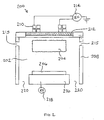
- Fig. 5 illustrates a multi-layered coupling window arrangement 500, in accordance with one embodiment of the present invention.
- the multi-layered coupling window arrangement 500 may respectively correspond to the coupling window 212 illustrated in Fig. 2 .
- Multi-layered coupling window 500 includes at least a first layer 504 and a second layer 506.
- first layer 504 is bonded to second layer 506.
- the two layers are thermally bonded together.
- a this is not a limitation and that other bonding processes may be used.
- second layer 506 preferably forms part of the inner peripheral surface of the process chamber.
- the second layer is configured to act as an electrostatic shield that reduces the potential difference on its surface.
- the second layer is arranged to be electrically isolated and preferably formed from a conducting or semi-conducting material that can facilitate the passage of inductive RF energy from the antenna to the plasma.
- the second layer is preferably formed from a material that is substantially resistant to a plasma.
- the second layer is formed from Silicon Carbide (SiC).
- SiC Silicon Carbide
- SiC Silicon Carbide
- SiC Silicon Carbide
- SiC Silicon Carbide
- the resistivity of the second layer is an important parameter for ensuring that the layer act as an electrostatic shield, while not impacting the inductive electric field.
- the particular resistivity range to be used in the invention depends on the exact dimensions of the antenna with which the coupling window is being used, the operating frequency of the power coupling and the thickness of the second layer.
- a resistivity from about 100ohm-cm to about 10kohm-cm works well.
- the resistivity can be configured to be greater than 10 6 ohm-cm to make the second layer (e.g., SiC) act more like a dielectric layer.
- a capacitive voltage divider is generally formed, for example, an upper part, which is formed by the dielectric first layer having a constant capacitance, and a lower part, which is formed by the conductive second layer and the chamber walls before ignition and the conductive second layer and the plasma after ignition.
- the lower part Before ignition the lower part has a small capacitance, and therefore there is a large voltage aiding ignition (e.g., in order to initiate the discharge, a capacitive electric field is typically necessary). After ignition the lower part has a large capacitance such that the voltage is substantially reduced, and therefore it does not lead to significant capacitive power coupling.
- the first layer is preferably formed from a dielectric material that can facilitate the passage of inductive RF energy from the antenna to the plasma. Further, the first layer is configured to be strong enough to structurally hold vacuum and robust enough to be easily handled during periodic cleaning of the chamber. Additionally, the first layer is generally formed from a dielectric material that has superior thermal properties to enable temperature control of the window.
- dielectric materials formed from Silicon Nitride (SiN) or Aluminum Nitride (AlN) work well. However, it should be understood that this is not a limitation and that other materials may be used. For example, alumina and quartz may also work well.
- the overall thickness of the multi-layer coupling window 500 is configured to be thin enough to effectively transmit the antenna RF energy to the plasma, while being sufficient to withstand the pressures and heat that are generated during processing.
- the thickness of the multi-layer coupling window is between 1.3 cm (0.5 inches) and 2.5 cm (1 inch). More preferably, the thickness of the multi-layer coupling window is about 2 cm (0.8 inches).
- the first layer 504 should have a thickness greater than the second layer 506.
- the thickness of the first layer is between 1.3 cm (0.5 inches) and 2.5 cm (1 inches). More preferably, the thickness of the first layer is about 1.5 cm (0.6 inches).
- the thickness of the second layer is preferably between 0.25 cm (0.1 inch) and 1.3 cm (0.5 inches). More preferably, the thickness of the second layer is about 0.5 cm (0.2 inches). It should be understood that the actual thickness of layers may vary according the specific material chosen for each layer.
- the second layer is configured to cover the entire first layer to protect the first layer from plasma exposure, and to ensure that pure materials (e.g., SiC) face the plasma region that is in contact with the substrate.
- pure materials e.g., SiC
- the second layer may be configured to cover only those portions of the first layer that face the plasma near the antenna.
- the size of the coupling window be equal to the size of the plasma processing chamber. In general, however, a small coupling window may reduce cost, particular when expensive materials such as SiC are employed.
- the shape of the window coupling is configured to coincide with the shape of the antenna arrangement, and therefore, the coupling window is configured to be substantially circular.
- the outer dimensions of the coupling window may be configured to extend a small distance beyond the outer dimensions of the antenna, in order to reduce any coupling to electrically conductive elements which may encircle the antenna.
- the outer dimensions of the coupling window is arranged to extend about 1 inch past the outer dimensions of the antenna.
- the coupling window may have a shape that is substantially the same as the antenna, i.e., hoop shaped.
- a lower dielectric constant e.g., less than about 10 tends to decrease the effects of the transmission line characteristics of the power coupling by reducing standing wave effects. More specifically, a lower dielectric constant tends to make the wavelength of the transmitted energy longer, which makes the antenna look shorter and therefore fewer nodes are created in the standing wave pattern. Accordingly, a lower dielectric constant tends to make any inherent azimuthally asymmetric coupling characteristic of an antenna less pronounced.
- the overall dielectric constant of the coupling window is preferably configured to be less than or equal to 10. It should be understood that the use of lower dielectric constants may not be required for all processes. In fact, a compromise between the desire for highly azimuthal symmetry and the simplicity of structural and thermal design is typically needed. However, if a high degree of uniformity is critical, the use of low dielectric constants can be quite beneficial. -
- the invention provides a coupling window that substantially reduces the capacitive coupling between the antenna and the plasma.
- variations in the plasma are substantially reduced.
- the inductive coupling coefficient is typically maintained, the ion bombardment of the coupling window is generally reduced, and more power is available for plasma generation, i.e., a higher plasma density for a given power.
- particle contamination associated with ion bombardment is generally reduced, and as a result, process variations associated with a varying thickness window (i.e., deposits or removed material) are decreased.
- the present invention utilizes pure materials, i.e., SiC, which tend to reduce process variations.
- a magnetic arrangement can be arranged with the multi-turn antenna to control the radial variation of the static magnetic field within the process chamber in the region proximate the coupling window and the multi-turn antenna.
- An example of such an magnetic arrangement may be found in co-pending WO 4137315 entitled, "IMPROVED PLASMA PROCESSING SYSTEMS AND METHODS THEREFOR".
Landscapes
- Physics & Mathematics (AREA)
- Engineering & Computer Science (AREA)
- Plasma & Fusion (AREA)
- Chemical & Material Sciences (AREA)
- Analytical Chemistry (AREA)
- Electromagnetism (AREA)
- Spectroscopy & Molecular Physics (AREA)
- Drying Of Semiconductors (AREA)
- Plasma Technology (AREA)
- Chemical Vapour Deposition (AREA)
Applications Claiming Priority (3)
| Application Number | Priority Date | Filing Date | Title |
|---|---|---|---|
| US440418 | 1995-05-12 | ||
| US09/440,418 US6320320B1 (en) | 1999-11-15 | 1999-11-15 | Method and apparatus for producing uniform process rates |
| PCT/US2000/042174 WO2001045134A2 (en) | 1999-11-15 | 2000-11-14 | Method and apparatus for producing uniform process rates |
Publications (2)
| Publication Number | Publication Date |
|---|---|
| EP1230668A2 EP1230668A2 (en) | 2002-08-14 |
| EP1230668B1 true EP1230668B1 (en) | 2012-11-07 |
Family
ID=23748690
Family Applications (1)
| Application Number | Title | Priority Date | Filing Date |
|---|---|---|---|
| EP00993006A Expired - Lifetime EP1230668B1 (en) | 1999-11-15 | 2000-11-14 | Plasma processing apparatus for producing uniform process rates |
Country Status (8)
| Country | Link |
|---|---|
| US (2) | US6320320B1 (ko) |
| EP (1) | EP1230668B1 (ko) |
| JP (2) | JP4758046B2 (ko) |
| KR (1) | KR100826488B1 (ko) |
| CN (1) | CN1227710C (ko) |
| AU (1) | AU4902801A (ko) |
| TW (1) | TW507253B (ko) |
| WO (1) | WO2001045134A2 (ko) |
Families Citing this family (255)
| Publication number | Priority date | Publication date | Assignee | Title |
|---|---|---|---|---|
| US6273022B1 (en) * | 1998-03-14 | 2001-08-14 | Applied Materials, Inc. | Distributed inductively-coupled plasma source |
| US6518705B2 (en) | 1999-11-15 | 2003-02-11 | Lam Research Corporation | Method and apparatus for producing uniform process rates |
| US6320320B1 (en) * | 1999-11-15 | 2001-11-20 | Lam Research Corporation | Method and apparatus for producing uniform process rates |
| US6744213B2 (en) * | 1999-11-15 | 2004-06-01 | Lam Research Corporation | Antenna for producing uniform process rates |
| EP1230664B1 (en) * | 1999-11-15 | 2008-05-07 | Lam Research Corporation | Processing systems |
| US6685798B1 (en) * | 2000-07-06 | 2004-02-03 | Applied Materials, Inc | Plasma reactor having a symmetrical parallel conductor coil antenna |
| US6694915B1 (en) * | 2000-07-06 | 2004-02-24 | Applied Materials, Inc | Plasma reactor having a symmetrical parallel conductor coil antenna |
| US7218739B2 (en) * | 2001-03-09 | 2007-05-15 | Microsoft Corporation | Multiple user authentication for online console-based gaming |
| US20020128061A1 (en) * | 2001-03-09 | 2002-09-12 | Blanco Victor Keith | Method and apparatus for restricting access to content in a gaming system |
| US20020128067A1 (en) * | 2001-03-09 | 2002-09-12 | Victor Keith Blanco | Method and apparatus for creating and playing soundtracks in a gaming system |
| US20020128068A1 (en) | 2001-03-09 | 2002-09-12 | Randall Whitten Jon Marcus | Method and apparatus for managing data in a gaming system |
| US20020137565A1 (en) * | 2001-03-09 | 2002-09-26 | Blanco Victor K. | Uniform media portal for a gaming system |
| US6527912B2 (en) * | 2001-03-30 | 2003-03-04 | Lam Research Corporation | Stacked RF excitation coil for inductive plasma processor |
| US20020170677A1 (en) * | 2001-04-07 | 2002-11-21 | Tucker Steven D. | RF power process apparatus and methods |
| US7203835B2 (en) * | 2001-11-13 | 2007-04-10 | Microsoft Corporation | Architecture for manufacturing authenticatable gaming systems |
| US7428638B1 (en) | 2001-11-13 | 2008-09-23 | Microsoft Corporation | Architecture for manufacturing authenticatable gaming systems |
| JP3823069B2 (ja) * | 2002-06-12 | 2006-09-20 | 株式会社アルバック | 磁気中性線放電プラズマ処理装置 |
| US6842147B2 (en) * | 2002-07-22 | 2005-01-11 | Lam Research Corporation | Method and apparatus for producing uniform processing rates |
| US6876155B2 (en) * | 2002-12-31 | 2005-04-05 | Lam Research Corporation | Plasma processor apparatus and method, and antenna |
| KR100964398B1 (ko) * | 2003-01-03 | 2010-06-17 | 삼성전자주식회사 | 유도결합형 안테나 및 이를 채용한 플라즈마 처리장치 |
| US6973554B2 (en) | 2003-04-23 | 2005-12-06 | Microsoft Corporation | Systems and methods for multiprocessor scalable write barrier |
| SG136148A1 (en) * | 2004-03-30 | 2007-10-29 | Adaptive Plasma Tech Corp | Plasma source coil and plasma chamber using the same |
| KR100530596B1 (ko) * | 2004-03-30 | 2005-11-23 | 어댑티브프라즈마테크놀로지 주식회사 | 웨이퍼 상에 높은 공정 균일도를 얻기 위한 플라즈마 소스코일을 채용하는 플라즈마 장비 |
| US8131955B2 (en) | 2004-04-15 | 2012-03-06 | Microsoft Corporation | Ephemeral garbage collection using a tracking mechanism on a card table to determine marked bundles |
| US7686926B2 (en) * | 2004-05-26 | 2010-03-30 | Applied Materials, Inc. | Multi-step process for forming a metal barrier in a sputter reactor |
| US7527713B2 (en) * | 2004-05-26 | 2009-05-05 | Applied Materials, Inc. | Variable quadruple electromagnet array in plasma processing |
| JP2006237479A (ja) * | 2005-02-28 | 2006-09-07 | Mitsubishi Heavy Ind Ltd | プラズマ処理装置 |
| US8956500B2 (en) * | 2007-04-24 | 2015-02-17 | Applied Materials, Inc. | Methods to eliminate “M-shape” etch rate profile in inductively coupled plasma reactor |
| JP2010050188A (ja) * | 2008-08-20 | 2010-03-04 | Panasonic Corp | プラズマドーピング装置 |
| US8319436B2 (en) * | 2009-02-02 | 2012-11-27 | Advanced Energy Industries, Inc. | Passive power distribution for multiple electrode inductive plasma source |
| JP5592098B2 (ja) | 2009-10-27 | 2014-09-17 | 東京エレクトロン株式会社 | プラズマ処理装置及びプラズマ処理方法 |
| US9313872B2 (en) | 2009-10-27 | 2016-04-12 | Tokyo Electron Limited | Plasma processing apparatus and plasma processing method |
| KR101757921B1 (ko) | 2009-10-27 | 2017-07-14 | 도쿄엘렉트론가부시키가이샤 | 플라즈마 처리 장치 및 플라즈마 처리 방법 |
| JP5554047B2 (ja) * | 2009-10-27 | 2014-07-23 | 東京エレクトロン株式会社 | プラズマ処理装置 |
| KR101757922B1 (ko) | 2009-10-27 | 2017-07-14 | 도쿄엘렉트론가부시키가이샤 | 플라즈마 처리 장치 |
| US8884178B2 (en) * | 2010-10-20 | 2014-11-11 | Lam Research Corporation | Methods and apparatus for igniting and sustaining plasma |
| US8659229B2 (en) * | 2011-05-16 | 2014-02-25 | Varian Semiconductor Equipment Associates, Inc. | Plasma attenuation for uniformity control |
| US20130023129A1 (en) | 2011-07-20 | 2013-01-24 | Asm America, Inc. | Pressure transmitter for a semiconductor processing environment |
| US9282624B2 (en) | 2011-09-16 | 2016-03-08 | Semes Co., Ltd. | Antenna structure and plasma generating device |
| US20140060738A1 (en) * | 2012-08-31 | 2014-03-06 | Semes Co., Ltd. | Apparatus for treating substrate |
| US10714315B2 (en) | 2012-10-12 | 2020-07-14 | Asm Ip Holdings B.V. | Semiconductor reaction chamber showerhead |
| US20160376700A1 (en) | 2013-02-01 | 2016-12-29 | Asm Ip Holding B.V. | System for treatment of deposition reactor |
| US11015245B2 (en) | 2014-03-19 | 2021-05-25 | Asm Ip Holding B.V. | Gas-phase reactor and system having exhaust plenum and components thereof |
| US10941490B2 (en) | 2014-10-07 | 2021-03-09 | Asm Ip Holding B.V. | Multiple temperature range susceptor, assembly, reactor and system including the susceptor, and methods of using the same |
| US10276355B2 (en) | 2015-03-12 | 2019-04-30 | Asm Ip Holding B.V. | Multi-zone reactor, system including the reactor, and method of using the same |
| US10458018B2 (en) | 2015-06-26 | 2019-10-29 | Asm Ip Holding B.V. | Structures including metal carbide material, devices including the structures, and methods of forming same |
| US10211308B2 (en) | 2015-10-21 | 2019-02-19 | Asm Ip Holding B.V. | NbMC layers |
| US11139308B2 (en) | 2015-12-29 | 2021-10-05 | Asm Ip Holding B.V. | Atomic layer deposition of III-V compounds to form V-NAND devices |
| US10529554B2 (en) | 2016-02-19 | 2020-01-07 | Asm Ip Holding B.V. | Method for forming silicon nitride film selectively on sidewalls or flat surfaces of trenches |
| US10367080B2 (en) | 2016-05-02 | 2019-07-30 | Asm Ip Holding B.V. | Method of forming a germanium oxynitride film |
| US11453943B2 (en) | 2016-05-25 | 2022-09-27 | Asm Ip Holding B.V. | Method for forming carbon-containing silicon/metal oxide or nitride film by ALD using silicon precursor and hydrocarbon precursor |
| US10612137B2 (en) | 2016-07-08 | 2020-04-07 | Asm Ip Holdings B.V. | Organic reactants for atomic layer deposition |
| US9859151B1 (en) | 2016-07-08 | 2018-01-02 | Asm Ip Holding B.V. | Selective film deposition method to form air gaps |
| KR102532607B1 (ko) | 2016-07-28 | 2023-05-15 | 에이에스엠 아이피 홀딩 비.브이. | 기판 가공 장치 및 그 동작 방법 |
| US9887082B1 (en) | 2016-07-28 | 2018-02-06 | Asm Ip Holding B.V. | Method and apparatus for filling a gap |
| US9812320B1 (en) | 2016-07-28 | 2017-11-07 | Asm Ip Holding B.V. | Method and apparatus for filling a gap |
| US11532757B2 (en) | 2016-10-27 | 2022-12-20 | Asm Ip Holding B.V. | Deposition of charge trapping layers |
| US10714350B2 (en) | 2016-11-01 | 2020-07-14 | ASM IP Holdings, B.V. | Methods for forming a transition metal niobium nitride film on a substrate by atomic layer deposition and related semiconductor device structures |
| KR102546317B1 (ko) | 2016-11-15 | 2023-06-21 | 에이에스엠 아이피 홀딩 비.브이. | 기체 공급 유닛 및 이를 포함하는 기판 처리 장치 |
| KR20180068582A (ko) | 2016-12-14 | 2018-06-22 | 에이에스엠 아이피 홀딩 비.브이. | 기판 처리 장치 |
| US11447861B2 (en) | 2016-12-15 | 2022-09-20 | Asm Ip Holding B.V. | Sequential infiltration synthesis apparatus and a method of forming a patterned structure |
| US11581186B2 (en) | 2016-12-15 | 2023-02-14 | Asm Ip Holding B.V. | Sequential infiltration synthesis apparatus |
| KR20180070971A (ko) | 2016-12-19 | 2018-06-27 | 에이에스엠 아이피 홀딩 비.브이. | 기판 처리 장치 |
| US10269558B2 (en) | 2016-12-22 | 2019-04-23 | Asm Ip Holding B.V. | Method of forming a structure on a substrate |
| US11390950B2 (en) | 2017-01-10 | 2022-07-19 | Asm Ip Holding B.V. | Reactor system and method to reduce residue buildup during a film deposition process |
| US10468261B2 (en) | 2017-02-15 | 2019-11-05 | Asm Ip Holding B.V. | Methods for forming a metallic film on a substrate by cyclical deposition and related semiconductor device structures |
| US10529563B2 (en) | 2017-03-29 | 2020-01-07 | Asm Ip Holdings B.V. | Method for forming doped metal oxide films on a substrate by cyclical deposition and related semiconductor device structures |
| US10770286B2 (en) | 2017-05-08 | 2020-09-08 | Asm Ip Holdings B.V. | Methods for selectively forming a silicon nitride film on a substrate and related semiconductor device structures |
| US11306395B2 (en) | 2017-06-28 | 2022-04-19 | Asm Ip Holding B.V. | Methods for depositing a transition metal nitride film on a substrate by atomic layer deposition and related deposition apparatus |
| US11615943B2 (en) | 2017-07-07 | 2023-03-28 | Advanced Energy Industries, Inc. | Inter-period control for passive power distribution of multiple electrode inductive plasma source |
| US11651939B2 (en) | 2017-07-07 | 2023-05-16 | Advanced Energy Industries, Inc. | Inter-period control system for plasma power delivery system and method of operating same |
| KR20190009245A (ko) | 2017-07-18 | 2019-01-28 | 에이에스엠 아이피 홀딩 비.브이. | 반도체 소자 구조물 형성 방법 및 관련된 반도체 소자 구조물 |
| US10541333B2 (en) | 2017-07-19 | 2020-01-21 | Asm Ip Holding B.V. | Method for depositing a group IV semiconductor and related semiconductor device structures |
| US11374112B2 (en) | 2017-07-19 | 2022-06-28 | Asm Ip Holding B.V. | Method for depositing a group IV semiconductor and related semiconductor device structures |
| US11018002B2 (en) | 2017-07-19 | 2021-05-25 | Asm Ip Holding B.V. | Method for selectively depositing a Group IV semiconductor and related semiconductor device structures |
| US10590535B2 (en) | 2017-07-26 | 2020-03-17 | Asm Ip Holdings B.V. | Chemical treatment, deposition and/or infiltration apparatus and method for using the same |
| US10692741B2 (en) | 2017-08-08 | 2020-06-23 | Asm Ip Holdings B.V. | Radiation shield |
| US10770336B2 (en) | 2017-08-08 | 2020-09-08 | Asm Ip Holding B.V. | Substrate lift mechanism and reactor including same |
| US11769682B2 (en) | 2017-08-09 | 2023-09-26 | Asm Ip Holding B.V. | Storage apparatus for storing cassettes for substrates and processing apparatus equipped therewith |
| US11139191B2 (en) | 2017-08-09 | 2021-10-05 | Asm Ip Holding B.V. | Storage apparatus for storing cassettes for substrates and processing apparatus equipped therewith |
| US11830730B2 (en) | 2017-08-29 | 2023-11-28 | Asm Ip Holding B.V. | Layer forming method and apparatus |
| KR102491945B1 (ko) | 2017-08-30 | 2023-01-26 | 에이에스엠 아이피 홀딩 비.브이. | 기판 처리 장치 |
| US11295980B2 (en) | 2017-08-30 | 2022-04-05 | Asm Ip Holding B.V. | Methods for depositing a molybdenum metal film over a dielectric surface of a substrate by a cyclical deposition process and related semiconductor device structures |
| US11056344B2 (en) | 2017-08-30 | 2021-07-06 | Asm Ip Holding B.V. | Layer forming method |
| US10658205B2 (en) | 2017-09-28 | 2020-05-19 | Asm Ip Holdings B.V. | Chemical dispensing apparatus and methods for dispensing a chemical to a reaction chamber |
| US10403504B2 (en) | 2017-10-05 | 2019-09-03 | Asm Ip Holding B.V. | Method for selectively depositing a metallic film on a substrate |
| CN109801824B (zh) * | 2017-11-15 | 2022-07-22 | 北京北方华创微电子装备有限公司 | 介质窗组件及反应腔室 |
| US11022879B2 (en) | 2017-11-24 | 2021-06-01 | Asm Ip Holding B.V. | Method of forming an enhanced unexposed photoresist layer |
| US11639811B2 (en) | 2017-11-27 | 2023-05-02 | Asm Ip Holding B.V. | Apparatus including a clean mini environment |
| KR102597978B1 (ko) | 2017-11-27 | 2023-11-06 | 에이에스엠 아이피 홀딩 비.브이. | 배치 퍼니스와 함께 사용하기 위한 웨이퍼 카세트를 보관하기 위한 보관 장치 |
| US10872771B2 (en) | 2018-01-16 | 2020-12-22 | Asm Ip Holding B. V. | Method for depositing a material film on a substrate within a reaction chamber by a cyclical deposition process and related device structures |
| TW202325889A (zh) | 2018-01-19 | 2023-07-01 | 荷蘭商Asm 智慧財產控股公司 | 沈積方法 |
| US11482412B2 (en) | 2018-01-19 | 2022-10-25 | Asm Ip Holding B.V. | Method for depositing a gap-fill layer by plasma-assisted deposition |
| US11081345B2 (en) | 2018-02-06 | 2021-08-03 | Asm Ip Holding B.V. | Method of post-deposition treatment for silicon oxide film |
| US10896820B2 (en) | 2018-02-14 | 2021-01-19 | Asm Ip Holding B.V. | Method for depositing a ruthenium-containing film on a substrate by a cyclical deposition process |
| WO2019158960A1 (en) | 2018-02-14 | 2019-08-22 | Asm Ip Holding B.V. | A method for depositing a ruthenium-containing film on a substrate by a cyclical deposition process |
| KR102636427B1 (ko) | 2018-02-20 | 2024-02-13 | 에이에스엠 아이피 홀딩 비.브이. | 기판 처리 방법 및 장치 |
| US10975470B2 (en) | 2018-02-23 | 2021-04-13 | Asm Ip Holding B.V. | Apparatus for detecting or monitoring for a chemical precursor in a high temperature environment |
| US11473195B2 (en) | 2018-03-01 | 2022-10-18 | Asm Ip Holding B.V. | Semiconductor processing apparatus and a method for processing a substrate |
| US11629406B2 (en) | 2018-03-09 | 2023-04-18 | Asm Ip Holding B.V. | Semiconductor processing apparatus comprising one or more pyrometers for measuring a temperature of a substrate during transfer of the substrate |
| US11114283B2 (en) | 2018-03-16 | 2021-09-07 | Asm Ip Holding B.V. | Reactor, system including the reactor, and methods of manufacturing and using same |
| KR102646467B1 (ko) | 2018-03-27 | 2024-03-11 | 에이에스엠 아이피 홀딩 비.브이. | 기판 상에 전극을 형성하는 방법 및 전극을 포함하는 반도체 소자 구조 |
| US11230766B2 (en) | 2018-03-29 | 2022-01-25 | Asm Ip Holding B.V. | Substrate processing apparatus and method |
| US11088002B2 (en) | 2018-03-29 | 2021-08-10 | Asm Ip Holding B.V. | Substrate rack and a substrate processing system and method |
| TWI811348B (zh) | 2018-05-08 | 2023-08-11 | 荷蘭商Asm 智慧財產控股公司 | 藉由循環沉積製程於基板上沉積氧化物膜之方法及相關裝置結構 |
| KR102596988B1 (ko) | 2018-05-28 | 2023-10-31 | 에이에스엠 아이피 홀딩 비.브이. | 기판 처리 방법 및 그에 의해 제조된 장치 |
| US11718913B2 (en) | 2018-06-04 | 2023-08-08 | Asm Ip Holding B.V. | Gas distribution system and reactor system including same |
| US11270899B2 (en) | 2018-06-04 | 2022-03-08 | Asm Ip Holding B.V. | Wafer handling chamber with moisture reduction |
| US11286562B2 (en) | 2018-06-08 | 2022-03-29 | Asm Ip Holding B.V. | Gas-phase chemical reactor and method of using same |
| KR102568797B1 (ko) | 2018-06-21 | 2023-08-21 | 에이에스엠 아이피 홀딩 비.브이. | 기판 처리 시스템 |
| US10797133B2 (en) | 2018-06-21 | 2020-10-06 | Asm Ip Holding B.V. | Method for depositing a phosphorus doped silicon arsenide film and related semiconductor device structures |
| JP2021529254A (ja) | 2018-06-27 | 2021-10-28 | エーエスエム・アイピー・ホールディング・ベー・フェー | 金属含有材料ならびに金属含有材料を含む膜および構造体を形成するための周期的堆積方法 |
| CN112292477A (zh) | 2018-06-27 | 2021-01-29 | Asm Ip私人控股有限公司 | 用于形成含金属的材料的循环沉积方法及包含含金属的材料的膜和结构 |
| US10612136B2 (en) | 2018-06-29 | 2020-04-07 | ASM IP Holding, B.V. | Temperature-controlled flange and reactor system including same |
| US10755922B2 (en) | 2018-07-03 | 2020-08-25 | Asm Ip Holding B.V. | Method for depositing silicon-free carbon-containing film as gap-fill layer by pulse plasma-assisted deposition |
| US10388513B1 (en) | 2018-07-03 | 2019-08-20 | Asm Ip Holding B.V. | Method for depositing silicon-free carbon-containing film as gap-fill layer by pulse plasma-assisted deposition |
| US11053591B2 (en) | 2018-08-06 | 2021-07-06 | Asm Ip Holding B.V. | Multi-port gas injection system and reactor system including same |
| US11430674B2 (en) | 2018-08-22 | 2022-08-30 | Asm Ip Holding B.V. | Sensor array, apparatus for dispensing a vapor phase reactant to a reaction chamber and related methods |
| KR20200030162A (ko) | 2018-09-11 | 2020-03-20 | 에이에스엠 아이피 홀딩 비.브이. | 박막 증착 방법 |
| US11024523B2 (en) | 2018-09-11 | 2021-06-01 | Asm Ip Holding B.V. | Substrate processing apparatus and method |
| US11049751B2 (en) | 2018-09-14 | 2021-06-29 | Asm Ip Holding B.V. | Cassette supply system to store and handle cassettes and processing apparatus equipped therewith |
| CN110970344A (zh) | 2018-10-01 | 2020-04-07 | Asm Ip控股有限公司 | 衬底保持设备、包含所述设备的系统及其使用方法 |
| US11232963B2 (en) | 2018-10-03 | 2022-01-25 | Asm Ip Holding B.V. | Substrate processing apparatus and method |
| KR102592699B1 (ko) | 2018-10-08 | 2023-10-23 | 에이에스엠 아이피 홀딩 비.브이. | 기판 지지 유닛 및 이를 포함하는 박막 증착 장치와 기판 처리 장치 |
| KR102546322B1 (ko) | 2018-10-19 | 2023-06-21 | 에이에스엠 아이피 홀딩 비.브이. | 기판 처리 장치 및 기판 처리 방법 |
| KR102605121B1 (ko) | 2018-10-19 | 2023-11-23 | 에이에스엠 아이피 홀딩 비.브이. | 기판 처리 장치 및 기판 처리 방법 |
| USD948463S1 (en) | 2018-10-24 | 2022-04-12 | Asm Ip Holding B.V. | Susceptor for semiconductor substrate supporting apparatus |
| US11087997B2 (en) | 2018-10-31 | 2021-08-10 | Asm Ip Holding B.V. | Substrate processing apparatus for processing substrates |
| KR20200051105A (ko) * | 2018-11-02 | 2020-05-13 | 에이에스엠 아이피 홀딩 비.브이. | 기판 지지 유닛 및 이를 포함하는 기판 처리 장치 |
| US11572620B2 (en) | 2018-11-06 | 2023-02-07 | Asm Ip Holding B.V. | Methods for selectively depositing an amorphous silicon film on a substrate |
| US11031242B2 (en) | 2018-11-07 | 2021-06-08 | Asm Ip Holding B.V. | Methods for depositing a boron doped silicon germanium film |
| US10818758B2 (en) | 2018-11-16 | 2020-10-27 | Asm Ip Holding B.V. | Methods for forming a metal silicate film on a substrate in a reaction chamber and related semiconductor device structures |
| US10847366B2 (en) | 2018-11-16 | 2020-11-24 | Asm Ip Holding B.V. | Methods for depositing a transition metal chalcogenide film on a substrate by a cyclical deposition process |
| US11217444B2 (en) | 2018-11-30 | 2022-01-04 | Asm Ip Holding B.V. | Method for forming an ultraviolet radiation responsive metal oxide-containing film |
| KR102636428B1 (ko) | 2018-12-04 | 2024-02-13 | 에이에스엠 아이피 홀딩 비.브이. | 기판 처리 장치를 세정하는 방법 |
| US11158513B2 (en) | 2018-12-13 | 2021-10-26 | Asm Ip Holding B.V. | Methods for forming a rhenium-containing film on a substrate by a cyclical deposition process and related semiconductor device structures |
| JP2020096183A (ja) | 2018-12-14 | 2020-06-18 | エーエスエム・アイピー・ホールディング・ベー・フェー | 窒化ガリウムの選択的堆積を用いてデバイス構造体を形成する方法及びそのためのシステム |
| JP7134104B2 (ja) * | 2019-01-09 | 2022-09-09 | 東京エレクトロン株式会社 | プラズマ処理装置およびプラズマ処理装置の載置台 |
| TWI819180B (zh) | 2019-01-17 | 2023-10-21 | 荷蘭商Asm 智慧財產控股公司 | 藉由循環沈積製程於基板上形成含過渡金屬膜之方法 |
| KR20200091543A (ko) | 2019-01-22 | 2020-07-31 | 에이에스엠 아이피 홀딩 비.브이. | 기판 처리 장치 |
| CN111524788B (zh) | 2019-02-01 | 2023-11-24 | Asm Ip私人控股有限公司 | 氧化硅的拓扑选择性膜形成的方法 |
| KR102638425B1 (ko) | 2019-02-20 | 2024-02-21 | 에이에스엠 아이피 홀딩 비.브이. | 기판 표면 내에 형성된 오목부를 충진하기 위한 방법 및 장치 |
| JP2020136677A (ja) | 2019-02-20 | 2020-08-31 | エーエスエム・アイピー・ホールディング・ベー・フェー | 基材表面内に形成された凹部を充填するための周期的堆積方法および装置 |
| US11482533B2 (en) | 2019-02-20 | 2022-10-25 | Asm Ip Holding B.V. | Apparatus and methods for plug fill deposition in 3-D NAND applications |
| KR102626263B1 (ko) | 2019-02-20 | 2024-01-16 | 에이에스엠 아이피 홀딩 비.브이. | 처리 단계를 포함하는 주기적 증착 방법 및 이를 위한 장치 |
| JP2020133004A (ja) | 2019-02-22 | 2020-08-31 | エーエスエム・アイピー・ホールディング・ベー・フェー | 基材を処理するための基材処理装置および方法 |
| KR20200108243A (ko) | 2019-03-08 | 2020-09-17 | 에이에스엠 아이피 홀딩 비.브이. | SiOC 층을 포함한 구조체 및 이의 형성 방법 |
| KR20200108242A (ko) | 2019-03-08 | 2020-09-17 | 에이에스엠 아이피 홀딩 비.브이. | 실리콘 질화물 층을 선택적으로 증착하는 방법, 및 선택적으로 증착된 실리콘 질화물 층을 포함하는 구조체 |
| US11742198B2 (en) | 2019-03-08 | 2023-08-29 | Asm Ip Holding B.V. | Structure including SiOCN layer and method of forming same |
| JP2020167398A (ja) | 2019-03-28 | 2020-10-08 | エーエスエム・アイピー・ホールディング・ベー・フェー | ドアオープナーおよびドアオープナーが提供される基材処理装置 |
| KR20200116855A (ko) | 2019-04-01 | 2020-10-13 | 에이에스엠 아이피 홀딩 비.브이. | 반도체 소자를 제조하는 방법 |
| US11447864B2 (en) | 2019-04-19 | 2022-09-20 | Asm Ip Holding B.V. | Layer forming method and apparatus |
| KR20200125453A (ko) | 2019-04-24 | 2020-11-04 | 에이에스엠 아이피 홀딩 비.브이. | 기상 반응기 시스템 및 이를 사용하는 방법 |
| KR20200130121A (ko) | 2019-05-07 | 2020-11-18 | 에이에스엠 아이피 홀딩 비.브이. | 딥 튜브가 있는 화학물질 공급원 용기 |
| KR20200130118A (ko) | 2019-05-07 | 2020-11-18 | 에이에스엠 아이피 홀딩 비.브이. | 비정질 탄소 중합체 막을 개질하는 방법 |
| KR20200130652A (ko) | 2019-05-10 | 2020-11-19 | 에이에스엠 아이피 홀딩 비.브이. | 표면 상에 재료를 증착하는 방법 및 본 방법에 따라 형성된 구조 |
| JP2020188255A (ja) | 2019-05-16 | 2020-11-19 | エーエスエム アイピー ホールディング ビー.ブイ. | ウェハボートハンドリング装置、縦型バッチ炉および方法 |
| USD975665S1 (en) | 2019-05-17 | 2023-01-17 | Asm Ip Holding B.V. | Susceptor shaft |
| USD947913S1 (en) | 2019-05-17 | 2022-04-05 | Asm Ip Holding B.V. | Susceptor shaft |
| USD935572S1 (en) | 2019-05-24 | 2021-11-09 | Asm Ip Holding B.V. | Gas channel plate |
| USD922229S1 (en) | 2019-06-05 | 2021-06-15 | Asm Ip Holding B.V. | Device for controlling a temperature of a gas supply unit |
| KR20200141002A (ko) | 2019-06-06 | 2020-12-17 | 에이에스엠 아이피 홀딩 비.브이. | 배기 가스 분석을 포함한 기상 반응기 시스템을 사용하는 방법 |
| KR20200143254A (ko) | 2019-06-11 | 2020-12-23 | 에이에스엠 아이피 홀딩 비.브이. | 개질 가스를 사용하여 전자 구조를 형성하는 방법, 상기 방법을 수행하기 위한 시스템, 및 상기 방법을 사용하여 형성되는 구조 |
| USD944946S1 (en) | 2019-06-14 | 2022-03-01 | Asm Ip Holding B.V. | Shower plate |
| USD931978S1 (en) | 2019-06-27 | 2021-09-28 | Asm Ip Holding B.V. | Showerhead vacuum transport |
| KR20210005515A (ko) | 2019-07-03 | 2021-01-14 | 에이에스엠 아이피 홀딩 비.브이. | 기판 처리 장치용 온도 제어 조립체 및 이를 사용하는 방법 |
| JP2021015791A (ja) | 2019-07-09 | 2021-02-12 | エーエスエム アイピー ホールディング ビー.ブイ. | 同軸導波管を用いたプラズマ装置、基板処理方法 |
| CN112216646A (zh) | 2019-07-10 | 2021-01-12 | Asm Ip私人控股有限公司 | 基板支撑组件及包括其的基板处理装置 |
| KR20210010307A (ko) | 2019-07-16 | 2021-01-27 | 에이에스엠 아이피 홀딩 비.브이. | 기판 처리 장치 |
| KR20210010820A (ko) | 2019-07-17 | 2021-01-28 | 에이에스엠 아이피 홀딩 비.브이. | 실리콘 게르마늄 구조를 형성하는 방법 |
| KR20210010816A (ko) | 2019-07-17 | 2021-01-28 | 에이에스엠 아이피 홀딩 비.브이. | 라디칼 보조 점화 플라즈마 시스템 및 방법 |
| US11643724B2 (en) | 2019-07-18 | 2023-05-09 | Asm Ip Holding B.V. | Method of forming structures using a neutral beam |
| CN112242296A (zh) | 2019-07-19 | 2021-01-19 | Asm Ip私人控股有限公司 | 形成拓扑受控的无定形碳聚合物膜的方法 |
| TW202113936A (zh) | 2019-07-29 | 2021-04-01 | 荷蘭商Asm Ip私人控股有限公司 | 用於利用n型摻雜物及/或替代摻雜物選擇性沉積以達成高摻雜物併入之方法 |
| CN112309900A (zh) | 2019-07-30 | 2021-02-02 | Asm Ip私人控股有限公司 | 基板处理设备 |
| CN112309899A (zh) | 2019-07-30 | 2021-02-02 | Asm Ip私人控股有限公司 | 基板处理设备 |
| US11587814B2 (en) | 2019-07-31 | 2023-02-21 | Asm Ip Holding B.V. | Vertical batch furnace assembly |
| US11227782B2 (en) | 2019-07-31 | 2022-01-18 | Asm Ip Holding B.V. | Vertical batch furnace assembly |
| US11587815B2 (en) | 2019-07-31 | 2023-02-21 | Asm Ip Holding B.V. | Vertical batch furnace assembly |
| CN112323048B (zh) | 2019-08-05 | 2024-02-09 | Asm Ip私人控股有限公司 | 用于化学源容器的液位传感器 |
| USD965044S1 (en) | 2019-08-19 | 2022-09-27 | Asm Ip Holding B.V. | Susceptor shaft |
| USD965524S1 (en) | 2019-08-19 | 2022-10-04 | Asm Ip Holding B.V. | Susceptor support |
| JP2021031769A (ja) | 2019-08-21 | 2021-03-01 | エーエスエム アイピー ホールディング ビー.ブイ. | 成膜原料混合ガス生成装置及び成膜装置 |
| USD940837S1 (en) | 2019-08-22 | 2022-01-11 | Asm Ip Holding B.V. | Electrode |
| USD949319S1 (en) | 2019-08-22 | 2022-04-19 | Asm Ip Holding B.V. | Exhaust duct |
| USD930782S1 (en) | 2019-08-22 | 2021-09-14 | Asm Ip Holding B.V. | Gas distributor |
| KR20210024423A (ko) | 2019-08-22 | 2021-03-05 | 에이에스엠 아이피 홀딩 비.브이. | 홀을 구비한 구조체를 형성하기 위한 방법 |
| USD979506S1 (en) | 2019-08-22 | 2023-02-28 | Asm Ip Holding B.V. | Insulator |
| KR20210024420A (ko) | 2019-08-23 | 2021-03-05 | 에이에스엠 아이피 홀딩 비.브이. | 비스(디에틸아미노)실란을 사용하여 peald에 의해 개선된 품질을 갖는 실리콘 산화물 막을 증착하기 위한 방법 |
| US11286558B2 (en) | 2019-08-23 | 2022-03-29 | Asm Ip Holding B.V. | Methods for depositing a molybdenum nitride film on a surface of a substrate by a cyclical deposition process and related semiconductor device structures including a molybdenum nitride film |
| KR20210029090A (ko) | 2019-09-04 | 2021-03-15 | 에이에스엠 아이피 홀딩 비.브이. | 희생 캡핑 층을 이용한 선택적 증착 방법 |
| KR20210029663A (ko) | 2019-09-05 | 2021-03-16 | 에이에스엠 아이피 홀딩 비.브이. | 기판 처리 장치 |
| US11562901B2 (en) | 2019-09-25 | 2023-01-24 | Asm Ip Holding B.V. | Substrate processing method |
| CN112593212B (zh) | 2019-10-02 | 2023-12-22 | Asm Ip私人控股有限公司 | 通过循环等离子体增强沉积工艺形成拓扑选择性氧化硅膜的方法 |
| TW202129060A (zh) | 2019-10-08 | 2021-08-01 | 荷蘭商Asm Ip控股公司 | 基板處理裝置、及基板處理方法 |
| TW202115273A (zh) | 2019-10-10 | 2021-04-16 | 荷蘭商Asm Ip私人控股有限公司 | 形成光阻底層之方法及包括光阻底層之結構 |
| KR20210045930A (ko) | 2019-10-16 | 2021-04-27 | 에이에스엠 아이피 홀딩 비.브이. | 실리콘 산화물의 토폴로지-선택적 막의 형성 방법 |
| US11637014B2 (en) | 2019-10-17 | 2023-04-25 | Asm Ip Holding B.V. | Methods for selective deposition of doped semiconductor material |
| KR20210047808A (ko) | 2019-10-21 | 2021-04-30 | 에이에스엠 아이피 홀딩 비.브이. | 막을 선택적으로 에칭하기 위한 장치 및 방법 |
| US11646205B2 (en) | 2019-10-29 | 2023-05-09 | Asm Ip Holding B.V. | Methods of selectively forming n-type doped material on a surface, systems for selectively forming n-type doped material, and structures formed using same |
| KR20210054983A (ko) | 2019-11-05 | 2021-05-14 | 에이에스엠 아이피 홀딩 비.브이. | 도핑된 반도체 층을 갖는 구조체 및 이를 형성하기 위한 방법 및 시스템 |
| US11501968B2 (en) | 2019-11-15 | 2022-11-15 | Asm Ip Holding B.V. | Method for providing a semiconductor device with silicon filled gaps |
| KR20210062561A (ko) | 2019-11-20 | 2021-05-31 | 에이에스엠 아이피 홀딩 비.브이. | 기판의 표면 상에 탄소 함유 물질을 증착하는 방법, 상기 방법을 사용하여 형성된 구조물, 및 상기 구조물을 형성하기 위한 시스템 |
| US11450529B2 (en) | 2019-11-26 | 2022-09-20 | Asm Ip Holding B.V. | Methods for selectively forming a target film on a substrate comprising a first dielectric surface and a second metallic surface |
| CN112951697A (zh) | 2019-11-26 | 2021-06-11 | Asm Ip私人控股有限公司 | 基板处理设备 |
| CN112885692A (zh) | 2019-11-29 | 2021-06-01 | Asm Ip私人控股有限公司 | 基板处理设备 |
| CN112885693A (zh) | 2019-11-29 | 2021-06-01 | Asm Ip私人控股有限公司 | 基板处理设备 |
| JP2021090042A (ja) | 2019-12-02 | 2021-06-10 | エーエスエム アイピー ホールディング ビー.ブイ. | 基板処理装置、基板処理方法 |
| KR20210070898A (ko) | 2019-12-04 | 2021-06-15 | 에이에스엠 아이피 홀딩 비.브이. | 기판 처리 장치 |
| JP2021097227A (ja) | 2019-12-17 | 2021-06-24 | エーエスエム・アイピー・ホールディング・ベー・フェー | 窒化バナジウム層および窒化バナジウム層を含む構造体を形成する方法 |
| US11527403B2 (en) | 2019-12-19 | 2022-12-13 | Asm Ip Holding B.V. | Methods for filling a gap feature on a substrate surface and related semiconductor structures |
| JP2021109175A (ja) | 2020-01-06 | 2021-08-02 | エーエスエム・アイピー・ホールディング・ベー・フェー | ガス供給アセンブリ、その構成要素、およびこれを含む反応器システム |
| KR20210095050A (ko) | 2020-01-20 | 2021-07-30 | 에이에스엠 아이피 홀딩 비.브이. | 박막 형성 방법 및 박막 표면 개질 방법 |
| TW202130846A (zh) | 2020-02-03 | 2021-08-16 | 荷蘭商Asm Ip私人控股有限公司 | 形成包括釩或銦層的結構之方法 |
| TW202146882A (zh) | 2020-02-04 | 2021-12-16 | 荷蘭商Asm Ip私人控股有限公司 | 驗證一物品之方法、用於驗證一物品之設備、及用於驗證一反應室之系統 |
| US11776846B2 (en) | 2020-02-07 | 2023-10-03 | Asm Ip Holding B.V. | Methods for depositing gap filling fluids and related systems and devices |
| US11781243B2 (en) | 2020-02-17 | 2023-10-10 | Asm Ip Holding B.V. | Method for depositing low temperature phosphorous-doped silicon |
| TW202203344A (zh) | 2020-02-28 | 2022-01-16 | 荷蘭商Asm Ip控股公司 | 專用於零件清潔的系統 |
| KR20210116240A (ko) | 2020-03-11 | 2021-09-27 | 에이에스엠 아이피 홀딩 비.브이. | 조절성 접합부를 갖는 기판 핸들링 장치 |
| US11876356B2 (en) | 2020-03-11 | 2024-01-16 | Asm Ip Holding B.V. | Lockout tagout assembly and system and method of using same |
| CN113394086A (zh) | 2020-03-12 | 2021-09-14 | Asm Ip私人控股有限公司 | 用于制造具有目标拓扑轮廓的层结构的方法 |
| KR20210124042A (ko) | 2020-04-02 | 2021-10-14 | 에이에스엠 아이피 홀딩 비.브이. | 박막 형성 방법 |
| TW202146689A (zh) | 2020-04-03 | 2021-12-16 | 荷蘭商Asm Ip控股公司 | 阻障層形成方法及半導體裝置的製造方法 |
| TW202145344A (zh) | 2020-04-08 | 2021-12-01 | 荷蘭商Asm Ip私人控股有限公司 | 用於選擇性蝕刻氧化矽膜之設備及方法 |
| US11821078B2 (en) | 2020-04-15 | 2023-11-21 | Asm Ip Holding B.V. | Method for forming precoat film and method for forming silicon-containing film |
| KR20210132600A (ko) | 2020-04-24 | 2021-11-04 | 에이에스엠 아이피 홀딩 비.브이. | 바나듐, 질소 및 추가 원소를 포함한 층을 증착하기 위한 방법 및 시스템 |
| CN113555279A (zh) | 2020-04-24 | 2021-10-26 | Asm Ip私人控股有限公司 | 形成含氮化钒的层的方法及包含其的结构 |
| TW202146831A (zh) | 2020-04-24 | 2021-12-16 | 荷蘭商Asm Ip私人控股有限公司 | 垂直批式熔爐總成、及用於冷卻垂直批式熔爐之方法 |
| KR20210134226A (ko) | 2020-04-29 | 2021-11-09 | 에이에스엠 아이피 홀딩 비.브이. | 고체 소스 전구체 용기 |
| KR20210134869A (ko) | 2020-05-01 | 2021-11-11 | 에이에스엠 아이피 홀딩 비.브이. | Foup 핸들러를 이용한 foup의 빠른 교환 |
| KR20210141379A (ko) | 2020-05-13 | 2021-11-23 | 에이에스엠 아이피 홀딩 비.브이. | 반응기 시스템용 레이저 정렬 고정구 |
| TW202147383A (zh) | 2020-05-19 | 2021-12-16 | 荷蘭商Asm Ip私人控股有限公司 | 基材處理設備 |
| KR20210145078A (ko) | 2020-05-21 | 2021-12-01 | 에이에스엠 아이피 홀딩 비.브이. | 다수의 탄소 층을 포함한 구조체 및 이를 형성하고 사용하는 방법 |
| KR20210145080A (ko) | 2020-05-22 | 2021-12-01 | 에이에스엠 아이피 홀딩 비.브이. | 과산화수소를 사용하여 박막을 증착하기 위한 장치 |
| TW202201602A (zh) | 2020-05-29 | 2022-01-01 | 荷蘭商Asm Ip私人控股有限公司 | 基板處理方法 |
| TW202218133A (zh) | 2020-06-24 | 2022-05-01 | 荷蘭商Asm Ip私人控股有限公司 | 形成含矽層之方法 |
| TW202217953A (zh) | 2020-06-30 | 2022-05-01 | 荷蘭商Asm Ip私人控股有限公司 | 基板處理方法 |
| KR20220010438A (ko) | 2020-07-17 | 2022-01-25 | 에이에스엠 아이피 홀딩 비.브이. | 포토리소그래피에 사용하기 위한 구조체 및 방법 |
| TW202204662A (zh) | 2020-07-20 | 2022-02-01 | 荷蘭商Asm Ip私人控股有限公司 | 用於沉積鉬層之方法及系統 |
| TW202212623A (zh) | 2020-08-26 | 2022-04-01 | 荷蘭商Asm Ip私人控股有限公司 | 形成金屬氧化矽層及金屬氮氧化矽層的方法、半導體結構、及系統 |
| USD990534S1 (en) | 2020-09-11 | 2023-06-27 | Asm Ip Holding B.V. | Weighted lift pin |
| USD1012873S1 (en) | 2020-09-24 | 2024-01-30 | Asm Ip Holding B.V. | Electrode for semiconductor processing apparatus |
| TW202229613A (zh) | 2020-10-14 | 2022-08-01 | 荷蘭商Asm Ip私人控股有限公司 | 於階梯式結構上沉積材料的方法 |
| TW202217037A (zh) | 2020-10-22 | 2022-05-01 | 荷蘭商Asm Ip私人控股有限公司 | 沉積釩金屬的方法、結構、裝置及沉積總成 |
| TW202223136A (zh) | 2020-10-28 | 2022-06-16 | 荷蘭商Asm Ip私人控股有限公司 | 用於在基板上形成層之方法、及半導體處理系統 |
| KR20220076343A (ko) | 2020-11-30 | 2022-06-08 | 에이에스엠 아이피 홀딩 비.브이. | 기판 처리 장치의 반응 챔버 내에 배열되도록 구성된 인젝터 |
| US11946137B2 (en) | 2020-12-16 | 2024-04-02 | Asm Ip Holding B.V. | Runout and wobble measurement fixtures |
| TW202231903A (zh) | 2020-12-22 | 2022-08-16 | 荷蘭商Asm Ip私人控股有限公司 | 過渡金屬沉積方法、過渡金屬層、用於沉積過渡金屬於基板上的沉積總成 |
| KR20220094272A (ko) * | 2020-12-28 | 2022-07-06 | 세메스 주식회사 | 기판 처리 장치 |
| USD1023959S1 (en) | 2021-05-11 | 2024-04-23 | Asm Ip Holding B.V. | Electrode for substrate processing apparatus |
| USD980813S1 (en) | 2021-05-11 | 2023-03-14 | Asm Ip Holding B.V. | Gas flow control plate for substrate processing apparatus |
| USD980814S1 (en) | 2021-05-11 | 2023-03-14 | Asm Ip Holding B.V. | Gas distributor for substrate processing apparatus |
| USD981973S1 (en) | 2021-05-11 | 2023-03-28 | Asm Ip Holding B.V. | Reactor wall for substrate processing apparatus |
| USD990441S1 (en) | 2021-09-07 | 2023-06-27 | Asm Ip Holding B.V. | Gas flow control plate |
| US20240038557A1 (en) * | 2022-07-28 | 2024-02-01 | Applied Materials, Inc. | Methods and apparatus for processing a substrate |
Family Cites Families (34)
| Publication number | Priority date | Publication date | Assignee | Title |
|---|---|---|---|---|
| US4990229A (en) | 1989-06-13 | 1991-02-05 | Plasma & Materials Technologies, Inc. | High density plasma deposition and etching apparatus |
| US5429070A (en) | 1989-06-13 | 1995-07-04 | Plasma & Materials Technologies, Inc. | High density plasma deposition and etching apparatus |
| US5091049A (en) | 1989-06-13 | 1992-02-25 | Plasma & Materials Technologies, Inc. | High density plasma deposition and etching apparatus |
| US5421891A (en) | 1989-06-13 | 1995-06-06 | Plasma & Materials Technologies, Inc. | High density plasma deposition and etching apparatus |
| US5122251A (en) | 1989-06-13 | 1992-06-16 | Plasma & Materials Technologies, Inc. | High density plasma deposition and etching apparatus |
| US4948458A (en) | 1989-08-14 | 1990-08-14 | Lam Research Corporation | Method and apparatus for producing magnetically-coupled planar plasma |
| US6165311A (en) * | 1991-06-27 | 2000-12-26 | Applied Materials, Inc. | Inductively coupled RF plasma reactor having an overhead solenoidal antenna |
| US5226967A (en) | 1992-05-14 | 1993-07-13 | Lam Research Corporation | Plasma apparatus including dielectric window for inducing a uniform electric field in a plasma chamber |
| US5401350A (en) | 1993-03-08 | 1995-03-28 | Lsi Logic Corporation | Coil configurations for improved uniformity in inductively coupled plasma systems |
| US5430355A (en) * | 1993-07-30 | 1995-07-04 | Texas Instruments Incorporated | RF induction plasma source for plasma processing |
| US5587038A (en) | 1994-06-16 | 1996-12-24 | Princeton University | Apparatus and process for producing high density axially extending plasmas |
| US5540800A (en) | 1994-06-23 | 1996-07-30 | Applied Materials, Inc. | Inductively coupled high density plasma reactor for plasma assisted materials processing |
| JP3140934B2 (ja) * | 1994-08-23 | 2001-03-05 | 東京エレクトロン株式会社 | プラズマ装置 |
| US5643394A (en) * | 1994-09-16 | 1997-07-01 | Applied Materials, Inc. | Gas injection slit nozzle for a plasma process reactor |
| JP3153743B2 (ja) | 1995-08-31 | 2001-04-09 | 東京エレクトロン株式会社 | プラズマ処理装置 |
| JPH0982495A (ja) | 1995-09-18 | 1997-03-28 | Toshiba Corp | プラズマ生成装置およびプラズマ生成方法 |
| US6054013A (en) | 1996-02-02 | 2000-04-25 | Applied Materials, Inc. | Parallel plate electrode plasma reactor having an inductive antenna and adjustable radial distribution of plasma ion density |
| KR100469134B1 (ko) * | 1996-03-18 | 2005-09-02 | 비오이 하이디스 테크놀로지 주식회사 | 유도형플라즈마화학기상증착방법및그를이용하여생성된비정질실리콘박막트랜지스터 |
| US5669975A (en) | 1996-03-27 | 1997-09-23 | Sony Corporation | Plasma producing method and apparatus including an inductively-coupled plasma source |
| CA2207154A1 (en) | 1996-06-10 | 1997-12-10 | Lam Research Corporation | Inductively coupled source for deriving substantially uniform plasma flux |
| JP2845199B2 (ja) * | 1996-06-14 | 1999-01-13 | 日本電気株式会社 | ドライエッチング装置およびドライエッチング方法 |
| US6308654B1 (en) * | 1996-10-18 | 2001-10-30 | Applied Materials, Inc. | Inductively coupled parallel-plate plasma reactor with a conical dome |
| JP3940465B2 (ja) * | 1997-05-14 | 2007-07-04 | 株式会社アルバック | 反応性イオンエッチング装置 |
| US6103070A (en) * | 1997-05-14 | 2000-08-15 | Applied Materials, Inc. | Powered shield source for high density plasma |
| US5910221A (en) * | 1997-06-18 | 1999-06-08 | Applied Materials, Inc. | Bonded silicon carbide parts in a plasma reactor |
| US6028395A (en) | 1997-09-16 | 2000-02-22 | Lam Research Corporation | Vacuum plasma processor having coil with added conducting segments to its peripheral part |
| JPH11135438A (ja) * | 1997-10-28 | 1999-05-21 | Nippon Asm Kk | 半導体プラズマ処理装置 |
| US6028285A (en) * | 1997-11-19 | 2000-02-22 | Board Of Regents, The University Of Texas System | High density plasma source for semiconductor processing |
| US6164241A (en) * | 1998-06-30 | 2000-12-26 | Lam Research Corporation | Multiple coil antenna for inductively-coupled plasma generation systems |
| US6229264B1 (en) * | 1999-03-31 | 2001-05-08 | Lam Research Corporation | Plasma processor with coil having variable rf coupling |
| US6320320B1 (en) | 1999-11-15 | 2001-11-20 | Lam Research Corporation | Method and apparatus for producing uniform process rates |
| US6341574B1 (en) | 1999-11-15 | 2002-01-29 | Lam Research Corporation | Plasma processing systems |
| US6302966B1 (en) | 1999-11-15 | 2001-10-16 | Lam Research Corporation | Temperature control system for plasma processing apparatus |
| US6322661B1 (en) | 1999-11-15 | 2001-11-27 | Lam Research Corporation | Method and apparatus for controlling the volume of a plasma |
-
1999
- 1999-11-15 US US09/440,418 patent/US6320320B1/en not_active Expired - Lifetime
-
2000
- 2000-11-14 CN CNB008184070A patent/CN1227710C/zh not_active Expired - Lifetime
- 2000-11-14 WO PCT/US2000/042174 patent/WO2001045134A2/en active Application Filing
- 2000-11-14 AU AU49028/01A patent/AU4902801A/en not_active Abandoned
- 2000-11-14 JP JP2001545337A patent/JP4758046B2/ja not_active Expired - Lifetime
- 2000-11-14 KR KR1020027006166A patent/KR100826488B1/ko active IP Right Grant
- 2000-11-14 EP EP00993006A patent/EP1230668B1/en not_active Expired - Lifetime
- 2000-11-15 TW TW089124185A patent/TW507253B/zh not_active IP Right Cessation
-
2001
- 2001-10-12 US US09/977,569 patent/US6653791B1/en not_active Expired - Lifetime
-
2011
- 2011-04-21 JP JP2011095143A patent/JP5309179B2/ja not_active Expired - Lifetime
Also Published As
| Publication number | Publication date |
|---|---|
| CN1423827A (zh) | 2003-06-11 |
| TW507253B (en) | 2002-10-21 |
| AU4902801A (en) | 2001-06-25 |
| JP4758046B2 (ja) | 2011-08-24 |
| WO2001045134A2 (en) | 2001-06-21 |
| JP5309179B2 (ja) | 2013-10-09 |
| WO2001045134A9 (en) | 2002-11-14 |
| JP2011175977A (ja) | 2011-09-08 |
| KR100826488B1 (ko) | 2008-05-02 |
| CN1227710C (zh) | 2005-11-16 |
| JP2003517197A (ja) | 2003-05-20 |
| US6653791B1 (en) | 2003-11-25 |
| KR20020068346A (ko) | 2002-08-27 |
| EP1230668A2 (en) | 2002-08-14 |
| US6320320B1 (en) | 2001-11-20 |
| WO2001045134A3 (en) | 2002-02-07 |
Similar Documents
| Publication | Publication Date | Title |
|---|---|---|
| EP1230668B1 (en) | Plasma processing apparatus for producing uniform process rates | |
| US6873112B2 (en) | Method for producing a semiconductor device | |
| US6518705B2 (en) | Method and apparatus for producing uniform process rates | |
| US5429070A (en) | High density plasma deposition and etching apparatus | |
| KR100394484B1 (ko) | 플라즈마 처리 방법 및 장치 | |
| US6679981B1 (en) | Inductive plasma loop enhancing magnetron sputtering | |
| US5421891A (en) | High density plasma deposition and etching apparatus | |
| US10354841B2 (en) | Plasma generation and control using a DC ring | |
| US20140130926A1 (en) | Annular baffle | |
| TW202131371A (zh) | 蝕刻裝置及方法 | |
| US6432730B2 (en) | Plasma processing method and apparatus | |
| IL159935A (en) | Method and apparatus for producing uniform process rates | |
| KR102619012B1 (ko) | 다중 플라즈마 채널을 갖는 플라즈마 챔버 |
Legal Events
| Date | Code | Title | Description |
|---|---|---|---|
| PUAI | Public reference made under article 153(3) epc to a published international application that has entered the european phase |
Free format text: ORIGINAL CODE: 0009012 |
|
| 17P | Request for examination filed |
Effective date: 20020510 |
|
| AK | Designated contracting states |
Kind code of ref document: A2 Designated state(s): AT BE CH CY DE DK ES FI FR GB GR IE IT LI LU MC NL PT SE TR |
|
| AX | Request for extension of the european patent |
Free format text: AL;LT;LV;MK;RO;SI |
|
| RTI1 | Title (correction) |
Free format text: PLASMA PROCESSING APPARATUS FOR PRODUCING UNIFORM PROCESS RATES |
|
| GRAP | Despatch of communication of intention to grant a patent |
Free format text: ORIGINAL CODE: EPIDOSNIGR1 |
|
| GRAS | Grant fee paid |
Free format text: ORIGINAL CODE: EPIDOSNIGR3 |
|
| GRAA | (expected) grant |
Free format text: ORIGINAL CODE: 0009210 |
|
| AK | Designated contracting states |
Kind code of ref document: B1 Designated state(s): AT BE CH CY DE DK ES FI FR GB GR IE IT LI LU MC NL PT SE TR |
|
| REG | Reference to a national code |
Ref country code: GB Ref legal event code: FG4D |
|
| REG | Reference to a national code |
Ref country code: AT Ref legal event code: REF Ref document number: 583294 Country of ref document: AT Kind code of ref document: T Effective date: 20121115 Ref country code: CH Ref legal event code: EP |
|
| REG | Reference to a national code |
Ref country code: IE Ref legal event code: FG4D |
|
| REG | Reference to a national code |
Ref country code: DE Ref legal event code: R096 Ref document number: 60047625 Country of ref document: DE Effective date: 20130103 |
|
| REG | Reference to a national code |
Ref country code: AT Ref legal event code: MK05 Ref document number: 583294 Country of ref document: AT Kind code of ref document: T Effective date: 20121107 |
|
| REG | Reference to a national code |
Ref country code: NL Ref legal event code: VDEP Effective date: 20121107 |
|
| PG25 | Lapsed in a contracting state [announced via postgrant information from national office to epo] |
Ref country code: ES Free format text: LAPSE BECAUSE OF FAILURE TO SUBMIT A TRANSLATION OF THE DESCRIPTION OR TO PAY THE FEE WITHIN THE PRESCRIBED TIME-LIMIT Effective date: 20130218 Ref country code: NL Free format text: LAPSE BECAUSE OF FAILURE TO SUBMIT A TRANSLATION OF THE DESCRIPTION OR TO PAY THE FEE WITHIN THE PRESCRIBED TIME-LIMIT Effective date: 20121107 Ref country code: SE Free format text: LAPSE BECAUSE OF FAILURE TO SUBMIT A TRANSLATION OF THE DESCRIPTION OR TO PAY THE FEE WITHIN THE PRESCRIBED TIME-LIMIT Effective date: 20121107 Ref country code: FI Free format text: LAPSE BECAUSE OF FAILURE TO SUBMIT A TRANSLATION OF THE DESCRIPTION OR TO PAY THE FEE WITHIN THE PRESCRIBED TIME-LIMIT Effective date: 20121107 |
|
| PG25 | Lapsed in a contracting state [announced via postgrant information from national office to epo] |
Ref country code: BE Free format text: LAPSE BECAUSE OF FAILURE TO SUBMIT A TRANSLATION OF THE DESCRIPTION OR TO PAY THE FEE WITHIN THE PRESCRIBED TIME-LIMIT Effective date: 20121107 Ref country code: CY Free format text: LAPSE BECAUSE OF FAILURE TO SUBMIT A TRANSLATION OF THE DESCRIPTION OR TO PAY THE FEE WITHIN THE PRESCRIBED TIME-LIMIT Effective date: 20121107 Ref country code: PT Free format text: LAPSE BECAUSE OF FAILURE TO SUBMIT A TRANSLATION OF THE DESCRIPTION OR TO PAY THE FEE WITHIN THE PRESCRIBED TIME-LIMIT Effective date: 20130307 Ref country code: GR Free format text: LAPSE BECAUSE OF FAILURE TO SUBMIT A TRANSLATION OF THE DESCRIPTION OR TO PAY THE FEE WITHIN THE PRESCRIBED TIME-LIMIT Effective date: 20130208 |
|
| PG25 | Lapsed in a contracting state [announced via postgrant information from national office to epo] |
Ref country code: AT Free format text: LAPSE BECAUSE OF FAILURE TO SUBMIT A TRANSLATION OF THE DESCRIPTION OR TO PAY THE FEE WITHIN THE PRESCRIBED TIME-LIMIT Effective date: 20121107 |
|
| REG | Reference to a national code |
Ref country code: CH Ref legal event code: PL |
|
| PG25 | Lapsed in a contracting state [announced via postgrant information from national office to epo] |
Ref country code: LI Free format text: LAPSE BECAUSE OF NON-PAYMENT OF DUE FEES Effective date: 20121130 Ref country code: CH Free format text: LAPSE BECAUSE OF NON-PAYMENT OF DUE FEES Effective date: 20121130 Ref country code: DK Free format text: LAPSE BECAUSE OF FAILURE TO SUBMIT A TRANSLATION OF THE DESCRIPTION OR TO PAY THE FEE WITHIN THE PRESCRIBED TIME-LIMIT Effective date: 20121107 |
|
| REG | Reference to a national code |
Ref country code: IE Ref legal event code: MM4A |
|
| PG25 | Lapsed in a contracting state [announced via postgrant information from national office to epo] |
Ref country code: IT Free format text: LAPSE BECAUSE OF FAILURE TO SUBMIT A TRANSLATION OF THE DESCRIPTION OR TO PAY THE FEE WITHIN THE PRESCRIBED TIME-LIMIT Effective date: 20121107 |
|
| PLBE | No opposition filed within time limit |
Free format text: ORIGINAL CODE: 0009261 |
|
| STAA | Information on the status of an ep patent application or granted ep patent |
Free format text: STATUS: NO OPPOSITION FILED WITHIN TIME LIMIT |
|
| REG | Reference to a national code |
Ref country code: FR Ref legal event code: ST Effective date: 20130731 |
|
| 26N | No opposition filed |
Effective date: 20130808 |
|
| GBPC | Gb: european patent ceased through non-payment of renewal fee |
Effective date: 20130207 |
|
| PG25 | Lapsed in a contracting state [announced via postgrant information from national office to epo] |
Ref country code: IE Free format text: LAPSE BECAUSE OF NON-PAYMENT OF DUE FEES Effective date: 20121114 |
|
| PG25 | Lapsed in a contracting state [announced via postgrant information from national office to epo] |
Ref country code: FR Free format text: LAPSE BECAUSE OF NON-PAYMENT OF DUE FEES Effective date: 20130107 |
|
| REG | Reference to a national code |
Ref country code: DE Ref legal event code: R097 Ref document number: 60047625 Country of ref document: DE Effective date: 20130808 |
|
| PG25 | Lapsed in a contracting state [announced via postgrant information from national office to epo] |
Ref country code: GB Free format text: LAPSE BECAUSE OF NON-PAYMENT OF DUE FEES Effective date: 20130207 |
|
| PG25 | Lapsed in a contracting state [announced via postgrant information from national office to epo] |
Ref country code: MC Free format text: LAPSE BECAUSE OF NON-PAYMENT OF DUE FEES Effective date: 20121130 Ref country code: TR Free format text: LAPSE BECAUSE OF FAILURE TO SUBMIT A TRANSLATION OF THE DESCRIPTION OR TO PAY THE FEE WITHIN THE PRESCRIBED TIME-LIMIT Effective date: 20121107 |
|
| PG25 | Lapsed in a contracting state [announced via postgrant information from national office to epo] |
Ref country code: LU Free format text: LAPSE BECAUSE OF NON-PAYMENT OF DUE FEES Effective date: 20121114 |
|
| PGFP | Annual fee paid to national office [announced via postgrant information from national office to epo] |
Ref country code: DE Payment date: 20191127 Year of fee payment: 20 |
|
| REG | Reference to a national code |
Ref country code: DE Ref legal event code: R071 Ref document number: 60047625 Country of ref document: DE |