EP1225538A1 - Kontaktloser datenträger - Google Patents
Kontaktloser datenträger Download PDFInfo
- Publication number
- EP1225538A1 EP1225538A1 EP01926129A EP01926129A EP1225538A1 EP 1225538 A1 EP1225538 A1 EP 1225538A1 EP 01926129 A EP01926129 A EP 01926129A EP 01926129 A EP01926129 A EP 01926129A EP 1225538 A1 EP1225538 A1 EP 1225538A1
- Authority
- EP
- European Patent Office
- Prior art keywords
- data carrier
- antenna coil
- patterns
- pattern
- chip
- Prior art date
- Legal status (The legal status is an assumption and is not a legal conclusion. Google has not performed a legal analysis and makes no representation as to the accuracy of the status listed.)
- Granted
Links
Images


Classifications
-
- G—PHYSICS
- G06—COMPUTING; CALCULATING OR COUNTING
- G06K—GRAPHICAL DATA READING; PRESENTATION OF DATA; RECORD CARRIERS; HANDLING RECORD CARRIERS
- G06K19/00—Record carriers for use with machines and with at least a part designed to carry digital markings
- G06K19/06—Record carriers for use with machines and with at least a part designed to carry digital markings characterised by the kind of the digital marking, e.g. shape, nature, code
- G06K19/067—Record carriers with conductive marks, printed circuits or semiconductor circuit elements, e.g. credit or identity cards also with resonating or responding marks without active components
- G06K19/07—Record carriers with conductive marks, printed circuits or semiconductor circuit elements, e.g. credit or identity cards also with resonating or responding marks without active components with integrated circuit chips
- G06K19/077—Constructional details, e.g. mounting of circuits in the carrier
- G06K19/07749—Constructional details, e.g. mounting of circuits in the carrier the record carrier being capable of non-contact communication, e.g. constructional details of the antenna of a non-contact smart card
- G06K19/07773—Antenna details
- G06K19/07777—Antenna details the antenna being of the inductive type
- G06K19/07779—Antenna details the antenna being of the inductive type the inductive antenna being a coil
-
- G—PHYSICS
- G06—COMPUTING; CALCULATING OR COUNTING
- G06K—GRAPHICAL DATA READING; PRESENTATION OF DATA; RECORD CARRIERS; HANDLING RECORD CARRIERS
- G06K19/00—Record carriers for use with machines and with at least a part designed to carry digital markings
- G06K19/06—Record carriers for use with machines and with at least a part designed to carry digital markings characterised by the kind of the digital marking, e.g. shape, nature, code
- G06K19/067—Record carriers with conductive marks, printed circuits or semiconductor circuit elements, e.g. credit or identity cards also with resonating or responding marks without active components
- G06K19/07—Record carriers with conductive marks, printed circuits or semiconductor circuit elements, e.g. credit or identity cards also with resonating or responding marks without active components with integrated circuit chips
- G06K19/077—Constructional details, e.g. mounting of circuits in the carrier
- G06K19/07749—Constructional details, e.g. mounting of circuits in the carrier the record carrier being capable of non-contact communication, e.g. constructional details of the antenna of a non-contact smart card
- G06K19/07773—Antenna details
- G06K19/07777—Antenna details the antenna being of the inductive type
- G06K19/07779—Antenna details the antenna being of the inductive type the inductive antenna being a coil
- G06K19/07783—Antenna details the antenna being of the inductive type the inductive antenna being a coil the coil being planar
-
- G—PHYSICS
- G06—COMPUTING; CALCULATING OR COUNTING
- G06K—GRAPHICAL DATA READING; PRESENTATION OF DATA; RECORD CARRIERS; HANDLING RECORD CARRIERS
- G06K19/00—Record carriers for use with machines and with at least a part designed to carry digital markings
- G06K19/06—Record carriers for use with machines and with at least a part designed to carry digital markings characterised by the kind of the digital marking, e.g. shape, nature, code
- G06K19/067—Record carriers with conductive marks, printed circuits or semiconductor circuit elements, e.g. credit or identity cards also with resonating or responding marks without active components
- G06K19/07—Record carriers with conductive marks, printed circuits or semiconductor circuit elements, e.g. credit or identity cards also with resonating or responding marks without active components with integrated circuit chips
- G06K19/077—Constructional details, e.g. mounting of circuits in the carrier
- G06K19/07749—Constructional details, e.g. mounting of circuits in the carrier the record carrier being capable of non-contact communication, e.g. constructional details of the antenna of a non-contact smart card
- G06K19/07773—Antenna details
- G06K19/07777—Antenna details the antenna being of the inductive type
- G06K19/07784—Antenna details the antenna being of the inductive type the inductive antenna consisting of a plurality of coils stacked on top of one another
Definitions
- the present invention relates to an art of non-contact data carrier.
- the present invention relates to a data carrier device with a data carrier chip or data carrier module taking the form of on-chip coil.
- This sort of non-contact data carrier has memory in which various data can be stored, by which the control of non-contact data carrier can be made by means of non-contact communication with an external reader/writer. Therefore, the non-contact data carrier has been applied for various uses such as automatic sorting of packages with data carrier, control of goods in stock, prevention of theft of goods and others and production- and distribution control.
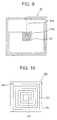
- FIG. 9 A conventional example of non-contact data carrier device with on-chip coil is shown in Fig. 9.
- the following method for supplying electric power from a booster antenna 51 to a data carrier chip taking the form of an on-chip coil 52 (the area surrounded by a frame shown by the dotted line) is employed: a booster antenna 51 is formed with a densely formed coil portion 51D and the data carrier chip taking the form of on-chip coil 52 is put on the densely formed coil portion 51D.
- the on-chip coil is mounted on the densely formed coil portion 51D in such a manner that the shape of on-chip coil accords with the shape of densely formed coil portion, to fabricate a data carrier.
- the most internal end of densely formed coil portion 51D is connected with the most external end of the first coil a through connection 51J. Therefore, it is needed to connect the most internal end of densely formed coil portion 51D with the connection 51J through a through hole or caulking precisely formed at the center of densely formed coil portion 51D.
- booster antenna 51 is not connected directly with on-chip coil 52, since booster antenna 51 and on-chip coil 52 are correspond to the first coil and the second coil, respectively.
- the on-chip coil has the small size with sides of about 3 to 5mm, while the densely formed coil portion corresponding to the on-chip coil has also the small size. Accordingly, there is a problem that to form through hole at the center of the densely formed coil portion is the highly precise work, so that the yield of products is decreased because of the difficulty in the location of through hole.
- a data carrier device comprising the structure of antenna in which there is a no problem in the location of a through hole in the above-mentioned non-contact data carrier.
- a first non-contact data carrier device is a non-contact data carrier device comprising an upper layer pattern having an antenna coil part made of wire pattern laid spirally and capacitor patterns and a lower layer pattern having, in a same way, an antenna coil part made of wire pattern laid spirally and capacitor patterns, wherein the respective antenna coil parts have almost the same external forms, and wherein the upper and lower layer patterns are disposed on a surface and a back of a dielectric layer, respectively, in such a manner that at least the external forms of the respective antenna coil parts accord with each other so that a resonance circuit is formed, characterized in that a part of each antenna coil part includes a portion which has the shape according with the external form of coil of a data carrier chip with on-chip coil and has a densely formed wire pattern, and that the data carrier chip is mounted on one of the portions of densely formed wire pattern in such a manner that the coil of data carrier chip partially conforms to the external form of the densely formed wire pattern. Since a part of each antenna coil part includes a portion which has the shape according with
- a second non-contact data carrier device is a non-contact data carrier device comprising an upper layer pattern having an antenna coil part made of wire pattern laid spirally and capacitor patterns and a lower layer pattern having, in a same way, an antenna coil part made of wire pattern laid spirally and capacitor patterns, wherein the respective antenna coil parts have almost the same external forms, and wherein the upper and lower layer patterns are disposed on a surface and a back of a dielectric layer, respectively, in such a manner that at least the external forms of the respective antenna coil parts accord with each other so that a resonance circuit is formed, characterized in that a part of each antenna coil part includes a portion which has the shape according with the external form of coil of a data carrier module with on-chip coil and has a densely formed wire pattern, and that the data carrier module is mounted on one of the portions of densely formed wire pattern in such a manner that the coil of data carrier module partially conforms to the external form of coil of the densely formed wire pattern. Since a data carrier device of the present invention is formed as mentioned here
- a third non-contact data carrier device is a non-contact data carrier device comprising an upper layer pattern having an antenna coil part made of wire pattern laid spirally and capacitor patterns and a lower layer pattern having, in a same way, an antenna coil part made of wire pattern laid spirally and capacitor patterns, wherein a part of each antenna coil part of the respective layer patterns includes a portion which has the shape according with the external form of coil of a data carrier chip with on-chip coil and has a densely formed wire pattern, and wherein the respective parts of antenna coil are formed into forms such that at least both the antenna coil parts are engaged with each other in the manner that one antenna coil is engaged with another antenna coil outward or inside another coil pattern except the respective capacitor patterns and the respective densely formed wire patterns, wherein the forms of capacitor patterns and the forms of densely formed wire patterns of both the layer patterns are almost the same, and wherein the upper and lower layer patterns are disposed on a surface and a back of a dielectric layer, respectively, in such a manner that the upper and lower layer patterns correspond to each other
- a fourth non-contact data carrier device is a non-contact data carrier device comprising an upper layer pattern having an antenna coil part made of wire pattern laid spirally and capacitor patterns and a lower layer pattern having, in a same way, an antenna coil part made of wire pattern laid spirally and capacitor patterns, wherein a part of each antenna coil part of the respective layer patterns includes a portion which has the shape according with the external form of coil included in, a data carrier chip with on-chip coil and has a densely formed wire pattern, wherein the respective parts of antenna coil are formed into forms such that at least both the antenna coil parts are engaged with each other in the manner that one antenna coil is engaged with another antenna coil outward or inside another coil pattern except the respective capacitor patterns and the respective densely formed wire patterns, wherein the forms of capacitor patterns and the forms of densely formed wire patterns of both the layer patterns are almost the same, and wherein the upper and lower layer patterns are disposed on a surface and a back of a dielectric layer, respectively, in such a manner that the upper and lower layer patterns corresponds to
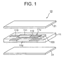
- Fig. 1 is an exploded perspective view of the first mode of the present invention.
- a non-contact data carrier device is usually comprised of antenna sheet 11 having an antenna coil parts and capacitor patterns, and upper and lower protective sheets 21, 31 for protecting the antenna sheet.
- Antenna sheet 11 is made of insulating substrate wherein an upper layer pattern 11u and a lower layer pattern 11d having antenna coil parts 111 and capacitor patterns 112, 113, respectively, are formed on both sides of the antenna sheet to form a LC resonance circuit.
- Data carrier chip or data carrier module 100 taking the form of on-chip coil is mounted on specified position in antenna coil part 111.
- Various kinds of information are stored into a memory of the data carrier chip or data carrier module.
- Material of a substrate of antenna sheet 11 is selected according to the object of use of data carrier, wherein a sheet of hard poly vinyl chloride, a sheet of polyester (PET), a sheet of polyimide, a sheet of glass epoxy resin and others, which have usually insulation property and act also as dielectric layers, are used as the materials of antenna sheet.
- the thickness of antenna sheet is 20 to 150 ⁇ m, preferably of 25 to 100 ⁇ m.
- Material composed of the substrate and foil of aluminum, Cu or iron with thickness of 5 to 50 ⁇ m laminated on both sides of the substrate is used wherein the foil of aluminum, Cu or iron is etched into the desired form to form the antenna coil part and a capacitor pattern.
- the same material as material of a substrate of antenna sheet 11 can be applied for protective sheets 21, 31, however low-priced material as paper can be also used.
- a data carrier device is used in the production or the process of distribution. Therefore, ornamental element is not much needed for the protective sheets except a case where the data carrier device is used with being carried as commuter pass. Since a data carrier device of small dimensions is desired except a case where the data carrier device is used for the special object, the data carrier device is produced in the size of unit less than 50mm ⁇ 50mm under ordinary circumstances.
- Fig. 2 is a view showing one example of an upper layer pattern and a lower layer pattern formed on an antenna sheet.
- upper layer pattern 11u and lower layer pattern 11d are put on both sides of the substrate of antenna sheet so that at least the external forms of the respective layer patterns accord with each other seeing in the vertical direction.
- Fig. 2 shows a state where upper layer pattern 11u and lower layer pattern 11d are juxtaposed on right and left sides with being separated from a state where at least the external forms of the respective layer patterns accord with each other seeing in the vertical direction.
- Upper layer pattern 11u and lower layer pattern 11d have antenna coil part 111 and capacitor patterns 112, 113, respectively.
- the capacitor patterns are comprised of capacitor pattern 112 arranged inside antenna coil part 111 and another capacitor pattern 113 arranged outside antenna coil part 111.
- the external form of antenna coil parts 111 of the upper and lower patterns are the same or nearly the same, wherein the winding directions of wound lines of the upper and lower layer patterns are opposite to each other in such a manner that if the winding direction of wound line of the upper layer pattern is clockwise, the winding direction of wound line of the lower layer pattern is counterclockwise.
- winding directions of both the wound lines should be set in such directions that the magnetic flux of the upper layer pattern and the magnetic flux of the lower layer flux does not cancel with each other since the directions of electric currents are opposite to each other in the upper and lower antenna coil parts 111.
- Winding directions of both the wound lines are opposite like this.
- the respective linear patterns in antenna coil parts can be arranged substantially at the same positions seeing in the vertical directions.
- both the layer patterns are put on both sides of the antenna sheet in such a manner that the external forms of antenna coil parts as well as the wire patterns of antenna coil parts in both the layer patterns accord with each other seeing in the vertical direction, because magnetic flux density produced by both the wire patterns of antenna coil parts can be made still higher thereby.
- Portions of antenna coil parts 111 are provided with portions 111p of densely formed antenna lines with the form according with the external forms of on-chip coil of data carrier chip or data carrier module mounted on the antenna coil part.
- portions 111p of densely formed antenna lines with the form according with the external forms of on-chip coil of data carrier chip or data carrier module mounted on the antenna coil part means that the form of portions 111p of densely formed antenna lines accords with at least two or three sides more than a half of sides of the external forms of on-chip coil.
- a rectangle drawn by dotted line designated "F" is the external form of data carrier chip or data carrier module, wherein this external form is expressed slightly larger than the external form of coil itself of chip.
- the object of "providing with portions 111p of densely formed antenna lines in portions of antenna coil parts 111" is to increase magnetic flux density in the portions of densely formed antenna lines corresponding to the position of coil of IC chip wherein an end portion of antenna coil part 111 is formed with a portion in which a part of wire pattern is densely formed so as to converge into the shape of " ⁇ " as shown in Fig. 2.
- Data carrier chip comprised of IC chip and on-chip coil forms a first resonance circuit, while antenna coil part 111 and capacitor pattern 112 forms a second resonance circuit. Resonance is produced in the second resonance circuit according to signal transmitted from external reader/writer and the signal is sent to the IC chip through the first resonance circuit. Further, resonance is produced in the second resonance circuit according to signal transmitted from on-chip coil and the signal is sent to the external reader/writer by the produced resonance.
- sending of signal to the external reader/writer is carried out in the same manner as in data carrier chip.
- Capacity coupling of the antenna coil part and capacitor patterns connected with internal terminal and external terminal of the antenna coil part forms a resonance circuit. Accordingly, the step for connecting between the upper layer pattern and the lower layer pattern through a through hole is unnecessary. Therefore, a data carrier device can be produced with high yield and low cost.
- antenna coil (particularly the form of an area for mounting chip) makes possible to provide a wider pad for connecting the upper layer pattern with the lower layer pattern.
- a use of one capacitor pattern as pad for connection makes the technique of connection such as the forming of a fine through hole unnecessary.
- the form of whole the antenna coil is not limited to a long shape as shown in Fig. 2.
- Antenna coil may be formed into rectangle or circle.
- an area for mounting a chip of "portion of dense antenna lines" is not restricted to that with the shape projecting toward the outside of antenna coil.
- An area for mounting a chip may be formed into that with the shape entering the inside of antenna coil.
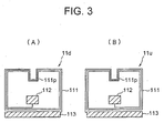
- Fig. 3 is a view showing an example in which an area for mounting a chip is formed into that with the shape entering the inside of antenna coil, wherein lower layer pattern 11d shown in Fig. 3(A) and upper layer pattern 11u shown in Fig. 3(B) are juxtaposed on left and right sides in the same manner as in Fig. 2.
- a data carrier device of the present invention has the advantage of the work for forming a through hole at the center of fine circuit of chip being unnecessary.
- the external form of whole the antenna coils is not restricted to that in which the external form of the upper layer pattern almost accords with the external form of lower layer pattern seeing in the vertical direction.
- One antenna coil may be engaged with another coil pattern outward or inside another coil pattern.
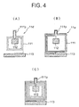
- Fig. 4 is a view for showing the form of antenna of the second mode of the present invention, wherein the figure shows an example in which antenna coil patterns of the upper and lower layers are engaged with each other.
- a case shown in the figure is an example in which the upper layer pattern 11u shown in Fig. 4(B) is engaged with the lower layer pattern 11d outside the lower layer pattern 11d shown in Fig. 4(A).
- Fig. 4(c) shows a state where the upper and lower layer patterns are put on both sides of the antenna sheet.
- capacitor patterns 112, 113 and areas 111p for mounting a chip in upper layer and lower layer are formed to overlap each other through the antenna sheet in the same manner as a case shown in Fig. 2.
- the first mode of the present invention is advantageous.
- FIG. 10 shows a conceptual view of data carrier chip taking the form of on-chip coil.
- a data carrier chip 100 comprises an antenna coil 102 formed into the rectangular coil on a substrate of conventional semiconductor device 101 so as to give the function of communication to IC chip, wherein the antenna coil 102 is provided with a pad 103 for connecting the antenna coil with IC chips at both terminals of the antenna coil.
- a case of data carrier module is in the same manner as in the data carrier chip. However, there is a difference in a point that IC chip and antenna coil produced separately are connected with each other so as to form module, wherein the IC chip and the antenna coil are not formed on the same semiconductor substrate. However, other effect is the same.
- a data carrier chip with on-chip coil itself has the function of communication.
- the object of mounting of data carrier chip on a booster antenna as in a non-contact data carrier device of the present invention is to increase the function of communication of chip with very small area antenna.
- the first and the third non-contact data carrier devices are non-contact data carrier modules with data carrier chip, and the second and the fourth data carrier devices are non-contact data carrier devices with data carrier module.
- Antenna line of data carrier chip or data carrier module is integrated with high density, wherein width of line and density of lines of antenna coil 102 do not correspond to the "portion 111p of densely formed wire pattern" of a non-contact data carrier device 10.
- providing the external form of the portion of antenna coil part and the external form of coil of the data carrier chip substantially the same contributes to increase the efficiency of magnetic connection between the chip and the portion of densely wire pattern.
- the form of portion of antenna coil of data carrier chip or data carrier module 100 is not restricted to rectangle.
- the form of antenna may be formed into circle or other form, wherein it is needed to set the external form of "the portion of densely formed wire pattern" to semicircle or other shape.
- Fig. 5 is a view showing another example of upper layer pattern and lower layer pattern formed on an antenna sheet, wherein upper layer pattern 11u and lower layer pattern 11d are juxtaposed on right and left sides in the same manner as in Fig. 2.
- the upper layer pattern and the lower layer pattern shown in Fig. 5 have antenna coil parts 111 and capacitor patterns 112, 113, respectively, in the same manner as in Fig. 2.
- the mode shown in Fig. 5 differs from the mode shown in Fig.2 in the point that the lower layer pattern 11d has capacitor pattern 112 provided inside antenna coil part 111 of the lower layer pattern 11d with nicks 112c in such a manner that the adjustment of wavelength (tuning) is possible.
- nicks 112c are provided in capacitor pattern 112 in order to facilitate the cutting out a part of capacitor pattern 112 and to use the nicks as a kind of scale of unit amount of adjustment.
- the adjustment of capacitor capacity is made in order to obtain a good state of communication by finely adjusting resonance frequency.
- Nicks 112c may be provided in any of the upper layer pattern and the lower layer pattern. However, it is advantageous to provide nicks on the side of face where the cut takes place. If any of capacitor patterns 112, 113 are cut, capacitor capacity can be reduced.
- any one of two of capacitor patterns provided inside or outside the antenna coil part are formed into the form in which the adjustment of wavelength is possible in such a manner, a change in micro wavelength produced by a change in conditions of production can be adjusted.
- the mode shown in Fig. 5 is characterized in that circular alignment marks 116 are provided for "the portion of dense antenna lines" on which data carrier chip or data carrier module is mounted.
- data carrier chip is mounted on the portion of dense antenna lines, for example, by means of mounting equipment such as flip chip bonder, wherein the chip is held to mounting equipment with locating the chip to the mounting equipment, image processing made by photographing the alignment mark 116 makes possible to mount the chip accurately at the fixed position.
- Antenna sheet can be also used under the state where capacitor pattern of upper layer and capacitor pattern of lower layers are connected with each other.
- outward condenser patterns of upper layer and lower layer are connected through a through-hole going through areas of the upper layer and lower layer corresponding to the outward capacitor pattern, for example positions 117 shown in Fig. 5 by evaporation and others.
- capacitor patterns of upper layer and lower layer are short-circuited so that the capacitor patterns lose the function of capacitor.
- Fig. 6 is a view showing further another example of upper layer pattern 11u and lower layer pattern 11d, wherein the upper layer pattern 11u and lower layer pattern 11d are juxtaposed on right and left sides in the same manner as in Fig. 2.
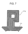
- the mode shown in Fig. 6 has antenna coil parts 111 and capacitor patterns 112, 113 in the same manner as in Fig. 2. However, the mode shown in Fig. 6 differs from the mode shown in Fig. 2 in the point that portion 11p for mounting a chip is formed into quadrangle with four sides as shown in Fig. 7 which is a partially enlarged view.
- Fig. 8 is a view showing an example in which portion for mounting a chip is provided inside antenna coil part and the portion for mounting a chip is formed into a quadrangle with four sides, wherein lower layer pattern 11d shown in Fig. 8(A) and upper layer pattern 11u shown in Fig. 8(B) are shown with being juxtaposed on upside and downside.
- the non-contact data carrier device comprises resonance circuit formed of antenna coils and capacitors, which sends and receives radio wave with a given frequency.
- bands of frequencies of 125kHz (medium wave), 13.56MHz, and 2.45Ghz(micro wave) can be used, wherein it is said that in case of 125kHz, the distance of communication is about 2cm and in case of 13.56MHz, the distance of communication is about 20cm.
- data carrier of with the area of 50mm ⁇ 50mm formed of conventional chip for antenna the distance of communication of 59 to 60cm can be obtained.
- An non-contact data carrier device was made experimentally using a substrate composed of polyethylene terephthalate having a thickness of 25 ⁇ m (Manufactured by TORAY Industries Inc.)and copper foils having a thickness of 30 ⁇ m laminated on both sides of polyethylene terephthalate.
- II iron
- the width of line of wire pattern of antenna coil formed by etching was 80 ⁇ m.
- Data carrier chip taking the form of on-chip coil with the size of 3mm ⁇ 3mm was mounted on a part formed into the shape of " ⁇ " of the antenna coil with precisely locating the position of data carrier chip to the position of the part formed into the shape of " ⁇ ".
- the chip was secured to the antenna coil by heating the chip while the chip being pressed to the antenna coil through adhesives to harden the adhesives.
- PET films having a thickness of 20 ⁇ m were laminated on both sides of substrate as the upper and lower protective sheets 21, 31, so that a non-contact data carrier device shown in Fig. 1 was formed.
- Reader/writer could receive/send radio wave with frequency of 13.56MHz from/to the formed non-contact data carrier device through the distance of communication of about 3cm even in case of weak output.
- a non-contact data carrier device of the present invention has an antenna coil having the above-mentioned form of antenna, the technique of connection such as forming a through-hole in fine part can be made unnecessary by changing the mounting part of chip from the form of wound line to the shape of " ⁇ " thereof.
- capacitor patterns provided at both terminals of antenna coil makes unnecessary to connect the upper and lower layer patterns by means of the technique of connection such as through-hole. Accordingly, the production of antenna with high yield and with low-cost production of antenna is made possible.
Landscapes
- Engineering & Computer Science (AREA)
- Computer Hardware Design (AREA)
- Microelectronics & Electronic Packaging (AREA)
- Physics & Mathematics (AREA)
- General Physics & Mathematics (AREA)
- Theoretical Computer Science (AREA)
- Computer Networks & Wireless Communication (AREA)
- Near-Field Transmission Systems (AREA)
- Credit Cards Or The Like (AREA)
- Inspection Of Paper Currency And Valuable Securities (AREA)
- Communication Cables (AREA)
- Details Of Aerials (AREA)
Applications Claiming Priority (3)
| Application Number | Priority Date | Filing Date | Title |
|---|---|---|---|
| JP2000140672 | 2000-05-12 | ||
| JP2000140672 | 2000-05-12 | ||
| PCT/JP2001/003815 WO2001085469A1 (fr) | 2000-05-12 | 2001-05-07 | Support de donnees sans contact |
Publications (3)
| Publication Number | Publication Date |
|---|---|
| EP1225538A1 true EP1225538A1 (de) | 2002-07-24 |
| EP1225538A4 EP1225538A4 (de) | 2003-09-10 |
| EP1225538B1 EP1225538B1 (de) | 2006-09-13 |
Family
ID=18647924
Family Applications (1)
| Application Number | Title | Priority Date | Filing Date |
|---|---|---|---|
| EP01926129A Expired - Lifetime EP1225538B1 (de) | 2000-05-12 | 2001-05-07 | Kontaktloser datenträger |
Country Status (6)
| Country | Link |
|---|---|
| US (1) | US6600219B2 (de) |
| EP (1) | EP1225538B1 (de) |
| JP (1) | JP4688396B2 (de) |
| AT (1) | ATE339740T1 (de) |
| DE (1) | DE60123004T2 (de) |
| WO (1) | WO2001085469A1 (de) |
Cited By (14)
| Publication number | Priority date | Publication date | Assignee | Title |
|---|---|---|---|---|
| WO2002097723A1 (en) * | 2001-05-31 | 2002-12-05 | Rafsec Oy | A smart label and a smart label web |
| WO2008012416A2 (fr) * | 2006-07-25 | 2008-01-31 | Oberthur Technologies | Entite electronique a microcircuit |
| FR2910152A1 (fr) * | 2006-12-19 | 2008-06-20 | Oberthur Card Syst Sa | Antenne avec pont sans via pour entite electronique portable |
| WO2014206579A1 (en) * | 2013-06-29 | 2014-12-31 | Féinics Amatech Teoranta | Booster antenna configurations and methods |
| US9033250B2 (en) | 2010-08-12 | 2015-05-19 | Féinics Amatech Teoranta | Dual interface smart cards, and methods of manufacturing |
| US9195932B2 (en) | 2010-08-12 | 2015-11-24 | Féinics Amatech Teoranta | Booster antenna configurations and methods |
| WO2015128188A3 (en) * | 2014-02-27 | 2015-12-23 | Féinics Amatech Teoranta | Rfid transponder chip modules |
| US9489613B2 (en) | 2011-08-08 | 2016-11-08 | Féinics Amatech Teoranta | RFID transponder chip modules with a band of the antenna extending inward |
| US9622359B2 (en) | 2011-08-08 | 2017-04-11 | Féinics Amatech Teoranta | RFID transponder chip modules |
| US9634391B2 (en) | 2011-08-08 | 2017-04-25 | Féinics Amatech Teoranta | RFID transponder chip modules |
| US10762413B2 (en) | 2012-08-30 | 2020-09-01 | Féinics Amatech Teoranta | Booster antenna configurations and methods |
| US10839282B2 (en) | 2014-03-08 | 2020-11-17 | Féinics Amatech Teoranta | RFID transponder chip modules, elements thereof, and methods |
| USD942538S1 (en) | 2020-07-30 | 2022-02-01 | Federal Card Services, LLC | Asymmetrical arrangement of contact pads and connection bridges of a transponder chip module |
| USD943024S1 (en) | 2020-07-30 | 2022-02-08 | Federal Card Services, LLC | Asymmetrical arrangement of contact pads and connection bridges of a transponder chip module |
Families Citing this family (20)
| Publication number | Priority date | Publication date | Assignee | Title |
|---|---|---|---|---|
| JP4058300B2 (ja) * | 2002-06-21 | 2008-03-05 | 株式会社日立製作所 | 携帯情報装置 |
| KR20040038134A (ko) * | 2002-10-31 | 2004-05-08 | 주식회사 쓰리비 시스템 | 안정된 비접촉 통신수단을 제공하는 콤비형 스마트 카드 |
| EP2164030A1 (de) * | 2004-01-29 | 2010-03-17 | YKK Corporation | Mit Identifikationsmedium ausgestatteter Artikel, Wahr-Falsch-Entscheidung an einem solchen Artikel und Güterverteilungssteuerverfahren |
| DE102006028827A1 (de) * | 2006-06-21 | 2008-01-10 | Dynamic Systems Gmbh | Transponder mit elektronischem Speicherchip und magnetischer Ringantenne |
| US8322624B2 (en) * | 2007-04-10 | 2012-12-04 | Feinics Amatech Teoranta | Smart card with switchable matching antenna |
| JP5118462B2 (ja) * | 2007-12-12 | 2013-01-16 | 日本発條株式会社 | コイルアンテナおよび非接触情報媒体 |
| EP2256672B1 (de) * | 2008-02-22 | 2016-04-13 | Toppan Printing Co., Ltd. | Transponder und buchform |
| WO2010087429A1 (ja) * | 2009-01-30 | 2010-08-05 | 株式会社村田製作所 | アンテナ及び無線icデバイス |
| JP5240293B2 (ja) * | 2009-04-02 | 2013-07-17 | 株式会社村田製作所 | 回路基板 |
| US9633304B2 (en) | 2010-08-12 | 2017-04-25 | Féinics Amatech Teoranta | Booster antenna configurations and methods |
| EP2525304A1 (de) * | 2011-05-17 | 2012-11-21 | Gemalto SA | Funkfrequenz-Transpondervorrichtung mit optimiertem passivem Resonanzkreis |
| US10867235B2 (en) * | 2011-08-08 | 2020-12-15 | Féinics Amatech Teoranta | Metallized smartcard constructions and methods |
| JP5365677B2 (ja) * | 2011-10-03 | 2013-12-11 | 大日本印刷株式会社 | 非接触式データキャリア装置 |
| EP2839536A1 (de) * | 2012-04-19 | 2015-02-25 | Smartrac IP B.V. | Integrierte schleifenstruktur für rfid |
| FR3001070B1 (fr) * | 2013-01-17 | 2016-05-06 | Inside Secure | Systeme d'antenne pour microcircuit sans contact |
| TWI560937B (en) * | 2013-11-22 | 2016-12-01 | Wistron Neweb Corp | Near field communication antenna |
| USD776070S1 (en) * | 2014-03-18 | 2017-01-10 | Sony Corporation | Non-contact type data carrier |
| US11514288B2 (en) * | 2014-08-10 | 2022-11-29 | Amatech Group Limited | Contactless metal card constructions |
| KR101659216B1 (ko) * | 2015-03-09 | 2016-09-22 | 삼성전기주식회사 | 코일 전자부품 및 그 제조방법 |
| JP2022133597A (ja) * | 2021-03-02 | 2022-09-14 | Tdk株式会社 | アンテナ装置及びこれを備えるアンテナモジュール |
Citations (3)
| Publication number | Priority date | Publication date | Assignee | Title |
|---|---|---|---|---|
| WO1997012263A2 (de) * | 1995-09-29 | 1997-04-03 | Siemens Aktiengesellschaft | Transponder und verfahren zur herstellung eines transponders |
| DE19811578A1 (de) * | 1998-03-17 | 1999-10-14 | Siemens Ag | Mehrlagige Leiterplatte sowie Verfahren zu deren Herstellung |
| FR2781588A1 (fr) * | 1998-07-21 | 2000-01-28 | Solaic Sa | Carte sans contact et procede de realisation d'une telle carte |
Family Cites Families (12)
| Publication number | Priority date | Publication date | Assignee | Title |
|---|---|---|---|---|
| JPS6359595A (ja) | 1986-08-30 | 1988-03-15 | 株式会社東芝 | 携帯可能媒体における実装方法 |
| JP3427663B2 (ja) * | 1996-06-18 | 2003-07-22 | 凸版印刷株式会社 | 非接触icカード |
| WO1998029261A1 (fr) * | 1996-12-26 | 1998-07-09 | Hitachi, Ltd. | Dispositif a semiconducteur et son procede de production |
| JP3900593B2 (ja) | 1997-05-27 | 2007-04-04 | 凸版印刷株式会社 | Icカードおよびicモジュール |
| JPH1131206A (ja) | 1997-07-10 | 1999-02-02 | Andeikusu:Kk | 共振ラベルおよびその製造方法 |
| FR2769109B1 (fr) * | 1997-09-26 | 1999-11-19 | Gemplus Sca | Dispositif electronique a puce jetable et procede de fabrication |
| TW424312B (en) * | 1998-03-17 | 2001-03-01 | Sanyo Electric Co | Module for IC cards, method for making a module for IC cards, hybrid integrated circuit module and method for making same |
| CA2343397C (en) * | 1998-09-11 | 2003-03-11 | Motorola, Inc. | Radio frequency identification tag apparatus and related method |
| US6404643B1 (en) * | 1998-10-15 | 2002-06-11 | Amerasia International Technology, Inc. | Article having an embedded electronic device, and method of making same |
| US6288905B1 (en) * | 1999-04-15 | 2001-09-11 | Amerasia International Technology Inc. | Contact module, as for a smart card, and method for making same |
| JP2000067197A (ja) * | 1999-07-16 | 2000-03-03 | Sony Corp | Icカ―ド |
| DE19950524A1 (de) * | 1999-10-20 | 2001-04-26 | Philips Corp Intellectual Pty | Chipkarte |
-
2001
- 2001-05-07 DE DE60123004T patent/DE60123004T2/de not_active Expired - Lifetime
- 2001-05-07 WO PCT/JP2001/003815 patent/WO2001085469A1/ja active IP Right Grant
- 2001-05-07 AT AT01926129T patent/ATE339740T1/de active
- 2001-05-07 US US10/030,450 patent/US6600219B2/en not_active Expired - Fee Related
- 2001-05-07 JP JP2001582101A patent/JP4688396B2/ja not_active Expired - Fee Related
- 2001-05-07 EP EP01926129A patent/EP1225538B1/de not_active Expired - Lifetime
Patent Citations (3)
| Publication number | Priority date | Publication date | Assignee | Title |
|---|---|---|---|---|
| WO1997012263A2 (de) * | 1995-09-29 | 1997-04-03 | Siemens Aktiengesellschaft | Transponder und verfahren zur herstellung eines transponders |
| DE19811578A1 (de) * | 1998-03-17 | 1999-10-14 | Siemens Ag | Mehrlagige Leiterplatte sowie Verfahren zu deren Herstellung |
| FR2781588A1 (fr) * | 1998-07-21 | 2000-01-28 | Solaic Sa | Carte sans contact et procede de realisation d'une telle carte |
Non-Patent Citations (1)
| Title |
|---|
| See also references of WO0185469A1 * |
Cited By (19)
| Publication number | Priority date | Publication date | Assignee | Title |
|---|---|---|---|---|
| WO2002097723A1 (en) * | 2001-05-31 | 2002-12-05 | Rafsec Oy | A smart label and a smart label web |
| WO2008012416A2 (fr) * | 2006-07-25 | 2008-01-31 | Oberthur Technologies | Entite electronique a microcircuit |
| FR2904453A1 (fr) * | 2006-07-25 | 2008-02-01 | Oberthur Card Syst Sa | Antenne electronique a microcircuit. |
| WO2008012416A3 (fr) * | 2006-07-25 | 2008-04-03 | Oberthur Card Syst Sa | Entite electronique a microcircuit |
| FR2910152A1 (fr) * | 2006-12-19 | 2008-06-20 | Oberthur Card Syst Sa | Antenne avec pont sans via pour entite electronique portable |
| WO2008090288A2 (fr) * | 2006-12-19 | 2008-07-31 | Oberthur Technologies | Antenne avec pont sans via pour entité électronique portable |
| WO2008090288A3 (fr) * | 2006-12-19 | 2008-10-16 | Oberthur Technologies | Antenne avec pont sans via pour entité électronique portable |
| US9033250B2 (en) | 2010-08-12 | 2015-05-19 | Féinics Amatech Teoranta | Dual interface smart cards, and methods of manufacturing |
| US9195932B2 (en) | 2010-08-12 | 2015-11-24 | Féinics Amatech Teoranta | Booster antenna configurations and methods |
| US9449269B2 (en) | 2010-08-12 | 2016-09-20 | Féinics Amatech Teoranta | Methods and apparatus for embedding wire in substrates for secure documents |
| US9489613B2 (en) | 2011-08-08 | 2016-11-08 | Féinics Amatech Teoranta | RFID transponder chip modules with a band of the antenna extending inward |
| US9622359B2 (en) | 2011-08-08 | 2017-04-11 | Féinics Amatech Teoranta | RFID transponder chip modules |
| US9634391B2 (en) | 2011-08-08 | 2017-04-25 | Féinics Amatech Teoranta | RFID transponder chip modules |
| US10762413B2 (en) | 2012-08-30 | 2020-09-01 | Féinics Amatech Teoranta | Booster antenna configurations and methods |
| WO2014206579A1 (en) * | 2013-06-29 | 2014-12-31 | Féinics Amatech Teoranta | Booster antenna configurations and methods |
| WO2015128188A3 (en) * | 2014-02-27 | 2015-12-23 | Féinics Amatech Teoranta | Rfid transponder chip modules |
| US10839282B2 (en) | 2014-03-08 | 2020-11-17 | Féinics Amatech Teoranta | RFID transponder chip modules, elements thereof, and methods |
| USD942538S1 (en) | 2020-07-30 | 2022-02-01 | Federal Card Services, LLC | Asymmetrical arrangement of contact pads and connection bridges of a transponder chip module |
| USD943024S1 (en) | 2020-07-30 | 2022-02-08 | Federal Card Services, LLC | Asymmetrical arrangement of contact pads and connection bridges of a transponder chip module |
Also Published As
| Publication number | Publication date |
|---|---|
| US6600219B2 (en) | 2003-07-29 |
| DE60123004D1 (de) | 2006-10-26 |
| EP1225538A4 (de) | 2003-09-10 |
| WO2001085469A1 (fr) | 2001-11-15 |
| DE60123004T2 (de) | 2006-12-21 |
| JP4688396B2 (ja) | 2011-05-25 |
| ATE339740T1 (de) | 2006-10-15 |
| US20020121685A1 (en) | 2002-09-05 |
| EP1225538B1 (de) | 2006-09-13 |
Similar Documents
| Publication | Publication Date | Title |
|---|---|---|
| EP1225538B1 (de) | Kontaktloser datenträger | |
| JP4641096B2 (ja) | 非接触式データキャリア装置とブースターアンテナ部用配線部材 | |
| US7078304B2 (en) | Method for producing an electrical circuit | |
| US8668151B2 (en) | Wireless IC device | |
| JP4052111B2 (ja) | 無線情報記憶媒体 | |
| EP1772927B1 (de) | Antenne und kontaktloses Etikett | |
| JP4173904B2 (ja) | 平坦な台から成る3次元アンテナアレイを有するセキュリティタグとその製作方法 | |
| EP2226893B1 (de) | IC-Funkgerät und IC-Funkgeräteteil | |
| EP1776662B1 (de) | Abstimmbare spiralantenne für sicherheitsetiketts | |
| EP1073009B1 (de) | Chipkarte | |
| AU2003243162A2 (en) | Method for producing an electrical circuit | |
| JP4205823B2 (ja) | Icカード | |
| JP2001101370A (ja) | 情報処理媒体 | |
| JP4562892B2 (ja) | 非接触式データキャリア装置とブースターアンテナ部用配線部材 | |
| JP4592872B2 (ja) | 非接触式データキャリア装置および補助アンテナ | |
| JP4184716B2 (ja) | 非接触式データキャリア装置用補助アンテナ部材を内蔵したカバンおよび非接触式データキャリア装置用補助アンテナ部材 | |
| US8720789B2 (en) | Wireless IC device | |
| JP4641095B2 (ja) | 非接触式データキャリア装置とブースターアンテナ部用配線部材 | |
| JP4743369B2 (ja) | 非接触式データキャリア装置用補助アンテナ部材、および該補助用アンテナ部材を配設した物品 | |
| JP2000259788A (ja) | 非接触icカードシステムおよび非接触icカードの外部読み書き装置 | |
| JP5023530B2 (ja) | 非接触式データキャリアおよび非接触式データキャリア用配線基材 | |
| KR20060132299A (ko) | 무선주파수 특성의 튜닝 방법 및 이를 사용하는 rfid태그 |
Legal Events
| Date | Code | Title | Description |
|---|---|---|---|
| PUAI | Public reference made under article 153(3) epc to a published international application that has entered the european phase |
Free format text: ORIGINAL CODE: 0009012 |
|
| 17P | Request for examination filed |
Effective date: 20020111 |
|
| AK | Designated contracting states |
Kind code of ref document: A1 Designated state(s): AT BE CH CY DE DK ES FI FR GB GR IE IT LI LU MC NL PT SE TR |
|
| A4 | Supplementary search report drawn up and despatched |
Effective date: 20030725 |
|
| RBV | Designated contracting states (corrected) |
Designated state(s): AT DE FR |
|
| 17Q | First examination report despatched |
Effective date: 20050204 |
|
| GRAP | Despatch of communication of intention to grant a patent |
Free format text: ORIGINAL CODE: EPIDOSNIGR1 |
|
| GRAS | Grant fee paid |
Free format text: ORIGINAL CODE: EPIDOSNIGR3 |
|
| GRAA | (expected) grant |
Free format text: ORIGINAL CODE: 0009210 |
|
| AK | Designated contracting states |
Kind code of ref document: B1 Designated state(s): AT DE FR |
|
| REF | Corresponds to: |
Ref document number: 60123004 Country of ref document: DE Date of ref document: 20061026 Kind code of ref document: P |
|
| ET | Fr: translation filed | ||
| PLBE | No opposition filed within time limit |
Free format text: ORIGINAL CODE: 0009261 |
|
| STAA | Information on the status of an ep patent application or granted ep patent |
Free format text: STATUS: NO OPPOSITION FILED WITHIN TIME LIMIT |
|
| 26N | No opposition filed |
Effective date: 20070614 |
|
| PGFP | Annual fee paid to national office [announced via postgrant information from national office to epo] |
Ref country code: AT Payment date: 20120511 Year of fee payment: 12 |
|
| PGFP | Annual fee paid to national office [announced via postgrant information from national office to epo] |
Ref country code: DE Payment date: 20130522 Year of fee payment: 13 |
|
| PGFP | Annual fee paid to national office [announced via postgrant information from national office to epo] |
Ref country code: FR Payment date: 20130603 Year of fee payment: 13 |
|
| REG | Reference to a national code |
Ref country code: DE Ref legal event code: R119 Ref document number: 60123004 Country of ref document: DE |
|
| REG | Reference to a national code |
Ref country code: AT Ref legal event code: MM01 Ref document number: 339740 Country of ref document: AT Kind code of ref document: T Effective date: 20140507 |
|
| REG | Reference to a national code |
Ref country code: DE Ref legal event code: R119 Ref document number: 60123004 Country of ref document: DE Effective date: 20141202 |
|
| PG25 | Lapsed in a contracting state [announced via postgrant information from national office to epo] |
Ref country code: AT Free format text: LAPSE BECAUSE OF NON-PAYMENT OF DUE FEES Effective date: 20140507 |
|
| REG | Reference to a national code |
Ref country code: FR Ref legal event code: ST Effective date: 20150130 |
|
| PG25 | Lapsed in a contracting state [announced via postgrant information from national office to epo] |
Ref country code: DE Free format text: LAPSE BECAUSE OF NON-PAYMENT OF DUE FEES Effective date: 20141202 |
|
| PG25 | Lapsed in a contracting state [announced via postgrant information from national office to epo] |
Ref country code: FR Free format text: LAPSE BECAUSE OF NON-PAYMENT OF DUE FEES Effective date: 20140602 |