EP1223621A2 - Verfahren zur Herstellung von eingebetteten nichtflüchtigen Halbleiterspeicherzellen - Google Patents
Verfahren zur Herstellung von eingebetteten nichtflüchtigen Halbleiterspeicherzellen Download PDFInfo
- Publication number
- EP1223621A2 EP1223621A2 EP01129956A EP01129956A EP1223621A2 EP 1223621 A2 EP1223621 A2 EP 1223621A2 EP 01129956 A EP01129956 A EP 01129956A EP 01129956 A EP01129956 A EP 01129956A EP 1223621 A2 EP1223621 A2 EP 1223621A2
- Authority
- EP
- European Patent Office
- Prior art keywords
- layer
- insulating layer
- area
- forming
- charge
- Prior art date
- Legal status (The legal status is an assumption and is not a legal conclusion. Google has not performed a legal analysis and makes no representation as to the accuracy of the status listed.)
- Granted
Links
- 239000004065 semiconductor Substances 0.000 title claims abstract description 24
- 238000004519 manufacturing process Methods 0.000 title claims abstract description 14
- 238000003860 storage Methods 0.000 claims abstract description 29
- 239000000758 substrate Substances 0.000 claims abstract description 17
- 238000000034 method Methods 0.000 claims description 22
- 238000009413 insulation Methods 0.000 claims description 6
- 238000003631 wet chemical etching Methods 0.000 claims description 4
- 238000001312 dry etching Methods 0.000 claims description 3
- GNFTZDOKVXKIBK-UHFFFAOYSA-N 3-(2-methoxyethoxy)benzohydrazide Chemical compound COCCOC1=CC=CC(C(=O)NN)=C1 GNFTZDOKVXKIBK-UHFFFAOYSA-N 0.000 claims 1
- FGUUSXIOTUKUDN-IBGZPJMESA-N C1(=CC=CC=C1)N1C2=C(NC([C@H](C1)NC=1OC(=NN=1)C1=CC=CC=C1)=O)C=CC=C2 Chemical compound C1(=CC=CC=C1)N1C2=C(NC([C@H](C1)NC=1OC(=NN=1)C1=CC=CC=C1)=O)C=CC=C2 FGUUSXIOTUKUDN-IBGZPJMESA-N 0.000 claims 1
- 210000000352 storage cell Anatomy 0.000 abstract 1
- 230000008878 coupling Effects 0.000 description 7
- 238000010168 coupling process Methods 0.000 description 7
- 238000005859 coupling reaction Methods 0.000 description 7
- 230000015572 biosynthetic process Effects 0.000 description 5
- 229910021420 polycrystalline silicon Inorganic materials 0.000 description 4
- 229920005591 polysilicon Polymers 0.000 description 4
- KRHYYFGTRYWZRS-UHFFFAOYSA-N Fluorane Chemical compound F KRHYYFGTRYWZRS-UHFFFAOYSA-N 0.000 description 3
- VYPSYNLAJGMNEJ-UHFFFAOYSA-N Silicium dioxide Chemical compound O=[Si]=O VYPSYNLAJGMNEJ-UHFFFAOYSA-N 0.000 description 3
- 230000015556 catabolic process Effects 0.000 description 3
- 238000002955 isolation Methods 0.000 description 3
- 239000000126 substance Substances 0.000 description 3
- XUIMIQQOPSSXEZ-UHFFFAOYSA-N Silicon Chemical compound [Si] XUIMIQQOPSSXEZ-UHFFFAOYSA-N 0.000 description 2
- 230000007547 defect Effects 0.000 description 2
- 239000000463 material Substances 0.000 description 2
- 229910052710 silicon Inorganic materials 0.000 description 2
- 239000010703 silicon Substances 0.000 description 2
- 229910004298 SiO 2 Inorganic materials 0.000 description 1
- BOTDANWDWHJENH-UHFFFAOYSA-N Tetraethyl orthosilicate Chemical compound CCO[Si](OCC)(OCC)OCC BOTDANWDWHJENH-UHFFFAOYSA-N 0.000 description 1
- 239000000969 carrier Substances 0.000 description 1
- 238000001311 chemical methods and process Methods 0.000 description 1
- 238000007796 conventional method Methods 0.000 description 1
- 230000001808 coupling effect Effects 0.000 description 1
- 239000013078 crystal Substances 0.000 description 1
- 238000005137 deposition process Methods 0.000 description 1
- 238000005530 etching Methods 0.000 description 1
- 230000002349 favourable effect Effects 0.000 description 1
- 238000011065 in-situ storage Methods 0.000 description 1
- 238000002347 injection Methods 0.000 description 1
- 239000007924 injection Substances 0.000 description 1
- 238000005468 ion implantation Methods 0.000 description 1
- 239000004922 lacquer Substances 0.000 description 1
- QPJSUIGXIBEQAC-UHFFFAOYSA-N n-(2,4-dichloro-5-propan-2-yloxyphenyl)acetamide Chemical compound CC(C)OC1=CC(NC(C)=O)=C(Cl)C=C1Cl QPJSUIGXIBEQAC-UHFFFAOYSA-N 0.000 description 1
- 150000004767 nitrides Chemical class 0.000 description 1
- 235000012239 silicon dioxide Nutrition 0.000 description 1
- 239000000377 silicon dioxide Substances 0.000 description 1
- 229910052814 silicon oxide Inorganic materials 0.000 description 1
Images


Classifications
-
- H—ELECTRICITY
- H10—SEMICONDUCTOR DEVICES; ELECTRIC SOLID-STATE DEVICES NOT OTHERWISE PROVIDED FOR
- H10B—ELECTRONIC MEMORY DEVICES
- H10B43/00—EEPROM devices comprising charge-trapping gate insulators
- H10B43/30—EEPROM devices comprising charge-trapping gate insulators characterised by the memory core region
-
- H—ELECTRICITY
- H10—SEMICONDUCTOR DEVICES; ELECTRIC SOLID-STATE DEVICES NOT OTHERWISE PROVIDED FOR
- H10B—ELECTRONIC MEMORY DEVICES
- H10B43/00—EEPROM devices comprising charge-trapping gate insulators
- H10B43/40—EEPROM devices comprising charge-trapping gate insulators characterised by the peripheral circuit region
-
- H—ELECTRICITY
- H10—SEMICONDUCTOR DEVICES; ELECTRIC SOLID-STATE DEVICES NOT OTHERWISE PROVIDED FOR
- H10D—INORGANIC ELECTRIC SEMICONDUCTOR DEVICES
- H10D64/00—Electrodes of devices having potential barriers
- H10D64/01—Manufacture or treatment
- H10D64/031—Manufacture or treatment of data-storage electrodes
- H10D64/037—Manufacture or treatment of data-storage electrodes comprising charge-trapping insulators
-
- Y—GENERAL TAGGING OF NEW TECHNOLOGICAL DEVELOPMENTS; GENERAL TAGGING OF CROSS-SECTIONAL TECHNOLOGIES SPANNING OVER SEVERAL SECTIONS OF THE IPC; TECHNICAL SUBJECTS COVERED BY FORMER USPC CROSS-REFERENCE ART COLLECTIONS [XRACs] AND DIGESTS
- Y10—TECHNICAL SUBJECTS COVERED BY FORMER USPC
- Y10S—TECHNICAL SUBJECTS COVERED BY FORMER USPC CROSS-REFERENCE ART COLLECTIONS [XRACs] AND DIGESTS
- Y10S438/00—Semiconductor device manufacturing: process
- Y10S438/981—Utilizing varying dielectric thickness
Definitions
- the present invention relates to a method for Manufacture of embedded non-volatile semiconductor memory cells and in particular to a manufacturing process of non-volatile memory cells in a semiconductor circuit with at least one high-voltage area and one logic area.
- non-volatile Semiconductor memory cells in semiconductor circuits which, for example, a logic part and a high voltage part have different types of transistors in the respective circuit parts or areas needed to the different, sometimes conflicting requirements to fulfill.
- transistors in one non-volatile storage area a tunnel layer, a charge storage Layer, a coupling layer and a control layer have so-called single or multi-transistor memory cells to realize.
- transistors in a logic part or logic area only from a gate oxide layer and a control layer, so that at least in Logic area the charge storage layer and the coupling layer must be replaced again.
- the invention is therefore based on the object of a method for the production of embedded non-volatile semiconductor memory cells to create a reliability with a Circuit is improved at least in a logic area.
- a first insulating layer a substrate in a high-voltage area, a storage area and a logic area, removing the first insulating layer in the storage area, forming a second one Isolation layer in the high-voltage, memory and logic area, one Forming and structuring a charge storage Layer with a third layer of insulation, removing the first to third insulating layer and the charge storage Layer in the logic area, forming a fourth Insulating layer, and forming and structuring one conductive control layer can be embedded non-volatile Semiconductor memory cells in a semiconductor circuit with a High-voltage area and a logic area designed in this way that the layers and electrical properties meet the highest demands, especially in the logic area become.
- the charge-storing device is preferably used first Structured layer and then the third insulating layer trained over the entire surface, resulting in a improved sidewall insulation for the charge storage Layer elements results and the charge holding times improved can be.
- the first insulating layer preferably consists of a 20th up to 25 nm thick oxide layer, on which an approx. 7 to 10 nm thick tunnel oxide layer is thermally formed.
- the first and the second insulating layer together result in one High voltage oxide layer for those in a high voltage range Switching elements or transistors.
- the charge storage layer consists of an electrical conductive or an electrically non-conductive layer, whereby different types of non-volatile semiconductor memory cells let it be realized.
- An ONO layer sequence is preferably used as the third insulating layer trained, the excellent coupling properties realized with easy manufacturability.
- the removal of the third insulating layer and the charge storage Layer is preferably dry etching carried out.
- wet chemical etching is performed, which in particular in the logic area to simple and cost effective way a high quality substrate surface can be exposed.
- the fourth insulation layer is made using conventional methods a gate oxide layer either thermally formed or deposited, which gives the reliability necessary for the logic part this insulating layer in terms of breakdown resistance receives.
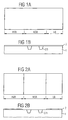
- Figures 1A and 1B show a respective top view and a Sectional view of a semiconductor circuit with a high voltage range or high-voltage range HVB, a non-volatile Memory area NSB and a logic area LB.
- non-volatile semiconductor memory cells are therefore intended in the non-volatile memory area NSB be trained, at the same time in the other high-voltage and logic areas corresponding to HVB and LB switching elements formed by high-voltage transistors and logic transistors should be. Since these switching elements as at the beginning Different and often even have already been discussed conflicting requirements will be described below a particularly advantageous processing in particular for the implementation of so-called embedded described nonvolatile semiconductor memory cells.
- the invention essentially refers to training of the first layers on a substrate, which is why Processing to form active areas and various doped wells in the substrate as well as on the formation "Upper" layer sequences are not discussed in more detail below becomes.
- a substrate 1 which for example is a silicon semiconductor substrate represents a first insulating layer 2 trained.
- the first insulating layer 2 can, for example be formed by a deposition process and preferably consists of a 20 to 25 nm thick silicon oxide layer. Alternatively, however, a thermal Training take place.
- the first insulating layer 2 in the non-volatile Storage area NSB removed locally.
- This structuring is, for example, with a lithographic, not shown Mask performed, using wet chemical or dry chemical processes a removal of first insulating layer 2 followed by lacquer stripping.
- a lithographic, not shown Mask performed, using wet chemical or dry chemical processes a removal of first insulating layer 2 followed by lacquer stripping.
- a second insulating layer 3 trained all over.
- this second insulating layer 3 in an oven process or by means of an RTP process (rapid thermal process) thermally formed, whereby preferably an approximately 7 to 10 nm thick tunnel oxide layer formed.
- This tunnel oxide layer becomes non-volatile Storage area as a tunnel layer for the respective non-volatile semiconductor memory cells used while especially in the HVB high-voltage area the first insulating layer 2 forms a high-voltage oxide layer 4, which has a thickness of approximately 25 to 35 nm. The reduced thickness essentially results from this Because of the reduced oxide growth on the first insulating layer Second
- FIGS. 4A and 4B there is now a full-surface formation and structuring a charge storage layer 5 with a third insulating layer 6, being according to one shown in Figure 4B first embodiment, the charge-storing Layer 5 over the whole area, for example as highly doped (in situ) Deposited polysilicon layer and then in vertical direction, for example above the trench insulation STI is structured.
- the third insulating layer 6 is formed over the whole area for example from an ONO layer sequence (oxide / nitride / Oxide) can exist.
- the third insulating layer 6 serves in particular in the non-volatile memory area NSB as a coupling layer and is also referred to as a coupling oxide layer.
- the side walls of the Strip-shaped charge storage layers 5 be particularly well insulated, which affects the charge holding ability of memory cells in a favorable manner.
- the ONO layer sequence for the third insulating layer 6 has a different dielectric than the coupling layer are used, in particular layers with high relative dielectric constant a reduction of Read / write voltages in the non-volatile memory area Favor NSB.
- Programming is preferably carried out here via Fowler-Nordheim tunnels or injection of hot load carriers through the second insulating layer 3 or tunnel oxide layer.
- first to third insulating layers 2, 3 and 6 and the charge storage layer 5 in the logic area LB removed.
- a dry chemical is preferably used first Etching the third insulating layer 6 and the charge storage Layer 5 performed that for example also together or simultaneously with the structuring of the charge-storing layer 5 and / or the third insulating layer 6 in the non-volatile memory part NSB according to figures 4A and 4B can be done.
- a wet-chemical etching of the logic region LB can be carried out.
- a fourth insulating layer 7 can be formed over the entire surface in a subsequent process step, which, particularly in the logic area, fully meets the high reliability requirements required in terms of breakdown resistance.
- this fourth insulating layer 7 is thermally formed as a gate oxide layer (SiO 2 ) by means of an oven process or RTP process. However, it can also be separated from the gas phase.
- a conductive control layer 8 is formed, for example an electrically conductive polysilicon layer is deposited and structured using, for example, a TEOS hard mask becomes. Alternatively, however, undoped polysilicon can also be used deposited and subsequently implanted or a metallic Layer to be deposited as a control layer 8.
- This control layer is preferred in the structuring 8 in the non-volatile memory area NSB at the same time the coupling layer or the third insulating layer 6 and the charge-storing layer 5 structured, whereby island-shaped charge-storing layer areas or non-volatile Semiconductor memory cells result. In the same way can also switch transistors in the high-voltage HVB range be formed.
- FIG. 5C shows a simplified sectional view according to one Section C-C 'of Figure 5A in a high voltage range, wherein a high-voltage transistor HVT now a stack of one Control layer 8, a fourth and third insulating layer 7 and 6, a charge storage layer 5 and a high-voltage oxide layer 4 exists.
- the charge storage Layer 5 removed in a previous step or short-circuited with the control layer 8.
- the Source areas S and drain areas D can be, for example formed at this time in the substrate 1 in a self-adjusting manner become. However, you can also go to a later or earlier one Time can be formed by various methods.
- FIG. 5D shows a sectional view according to a section D-D ' in Figure 5A, wherein a non-volatile memory transistor NST again from a control layer 8, a third and fourth Insulating layer 6 and 7, a charge storage layer 5 and a tunnel oxide layer or second insulating layer 3.
- FIG. 5E shows a simplified sectional view along a Section E-E 'according to Figure 5A in the logic area LB, wherein a switching transistor ST only a control layer 8 and an extremely high quality gate oxide layer as the fourth insulating layer 7 has.
- the invention has been described above on the basis of silicon semiconductor substrates described. However, it is not limited to this and similarly includes alternative substrate materials. In the same way, the invention is not based on the described silicon dioxide, polysilicon and ONO layers limited but includes alternatives in the same way Materials.
Landscapes
- Non-Volatile Memory (AREA)
- Semiconductor Memories (AREA)
Abstract
Description
Claims (11)
- Verfahren zur Herstellung von eingebetteten nichtflüchtigen Halbleiterspeicherzellen mit den Schritten:a) Ausbilden einer ersten Isolierschicht (2) auf einem Substrat (1) in einem Hochvoltbereich (HVB), einem Speicherbereich (NSB) und einem Logikbereich (LB);b) Entfernen der ersten Isolierschicht (2) im Speicherbereich (NSB);c) Ausbilden einer zweiten Isolierschicht (3) im Hochvoltbereich (HVB), Speicherbereich (NSB) und Logikbereich (LB);d) Ausbilden und Strukturieren einer ladungsspeichernden Schicht (5) mit einer dritten Isolierschicht (6) im Speicherbereich (NSB);e) Entfernen der ersten bis dritten Isolierschicht (2, 3, 6) sowie der ladungsspeichernden Schicht (5) im Logikbereich (LB);f) Ausbilden einer vierten Isolierschicht (7) im Hochvoltbereich (HVB), Speicherbereich (NSB) und Logikbereich (LB); undg) Ausbilden und Strukturieren einer leitenden Steuerschicht (8).
- Verfahren nach Patentanspruch 1,
dadurch gekennzeichnet, dass in Schritt d) nur die ladungsspeichernde Schicht (5) strukturiert wird und die dritte Isolierschicht (6) ganzflächig darauf ausgebildet wird. - Verfahren nach einem der Patentansprüche 1 oder 2,
dadurch gekennzeichnet, dass in Schritt a) eine 20 bis 25 nm dicke Oxidschicht abgeschieden wird. - Verfahren nach einem der Patentansprüche 1 bis 3,
dadurch gekennzeichnet, dass in Schritt c) eine ca. 7 bis 10 nm dicke Tunneloxidschicht thermisch ausgebildet wird. - Verfahren nach einem der Patentansprüche 1 bis 4,
dadurch gekennzeichnet, dass die erste und zweite Isolierschicht (2, 3) eine Hochvoltoxidschicht (4) ausbilden. - Verfahren nach einem der Patentansprüche 1 bis 5,
dadurch gekennzeichnet, dass in Schritt d) eine elektrisch leitende oder nicht leitende Schicht als ladungsspeichernde Schicht (5) ausgebildet wird. - Verfahren nach einem der Patentansprüche 1 bis 6,
dadurch gekennzeichnet, dass in Schritt d) eine ONO-Schichtenfolge als dritte Isolierschicht (6) ausgebildet wird. - Verfahren nach einem der Patentansprüche 1 bis 7,
dadurch gekennzeichnet, dass in Schritt e) ein Trockenätzen der dritten Isolierschicht (6) und der ladungsspeichernden Schicht (5) durchgeführt wird. - Verfahren nach einem der Patentansprüche 1 bis 8,
dadurch gekennzeichnet, dass in Schritt e) ein nasschemisches Ätzen der ersten und zweiten Isolierschicht (2, 3) durchgeführt wird. - Verfahren nach einem der Patentansprüche 1 bis 9,
dadurch gekennzeichnet, dass in Schritt f) eine Gateoxidschicht als vierte Isolierschicht (7) thermisch ausgebildet oder abgeschieden wird. - Verfahren nach einem der Patentansprüche 1 bis 10,
dadurch gekennzeichnet, dass das Strukturieren in Schritt g) mittels einer Hartmaske erfolgt.
Applications Claiming Priority (2)
| Application Number | Priority Date | Filing Date | Title |
|---|---|---|---|
| DE10101270 | 2001-01-12 | ||
| DE10101270A DE10101270A1 (de) | 2001-01-12 | 2001-01-12 | Verfahren zur Herstellung von eingebetteten nichtflüchtigen Halbleiterspeicherzellen |
Publications (3)
| Publication Number | Publication Date |
|---|---|
| EP1223621A2 true EP1223621A2 (de) | 2002-07-17 |
| EP1223621A3 EP1223621A3 (de) | 2005-08-17 |
| EP1223621B1 EP1223621B1 (de) | 2010-04-07 |
Family
ID=7670402
Family Applications (1)
| Application Number | Title | Priority Date | Filing Date |
|---|---|---|---|
| EP01129956A Expired - Lifetime EP1223621B1 (de) | 2001-01-12 | 2001-12-17 | Verfahren zur Herstellung von eingebetteten nichtflüchtigen Halbleiterspeicherzellen |
Country Status (4)
| Country | Link |
|---|---|
| US (1) | US6841448B2 (de) |
| EP (1) | EP1223621B1 (de) |
| CN (1) | CN1181535C (de) |
| DE (2) | DE10101270A1 (de) |
Families Citing this family (4)
| Publication number | Priority date | Publication date | Assignee | Title |
|---|---|---|---|---|
| KR100669345B1 (ko) * | 2005-10-28 | 2007-01-16 | 삼성전자주식회사 | 비휘발성 메모리 장치 및 그 형성 방법 |
| KR100833491B1 (ko) * | 2005-12-08 | 2008-05-29 | 한국전자통신연구원 | 임베디드 상변화 메모리 및 그 제조방법 |
| US7978504B2 (en) * | 2008-06-03 | 2011-07-12 | Infineon Technologies Ag | Floating gate device with graphite floating gate |
| CN103426747A (zh) * | 2012-05-14 | 2013-12-04 | 无锡华润上华科技有限公司 | 一种控制在炉管内生成的氧化层厚度的方法 |
Family Cites Families (13)
| Publication number | Priority date | Publication date | Assignee | Title |
|---|---|---|---|---|
| JPS56120166A (en) * | 1980-02-27 | 1981-09-21 | Hitachi Ltd | Semiconductor ic device and manufacture thereof |
| JP2664685B2 (ja) * | 1987-07-31 | 1997-10-15 | 株式会社東芝 | 半導体装置の製造方法 |
| CA2107602C (en) * | 1992-10-07 | 2004-01-20 | Andrew Jan Walker | Method of manufacturing an integrated circuit and integrated circuit obtained by this method |
| TW347567B (en) * | 1996-03-22 | 1998-12-11 | Philips Eloctronics N V | Semiconductor device and method of manufacturing a semiconductor device |
| US6121087A (en) * | 1996-06-18 | 2000-09-19 | Conexant Systems, Inc. | Integrated circuit device with embedded flash memory and method for manufacturing same |
| US5723355A (en) * | 1997-01-17 | 1998-03-03 | Programmable Microelectronics Corp. | Method to incorporate non-volatile memory and logic components into a single sub-0.3 micron fabrication process for embedded non-volatile memory |
| US6309975B1 (en) * | 1997-03-14 | 2001-10-30 | Micron Technology, Inc. | Methods of making implanted structures |
| US6194036B1 (en) * | 1997-10-20 | 2001-02-27 | The Regents Of The University Of California | Deposition of coatings using an atmospheric pressure plasma jet |
| US6667511B1 (en) * | 1997-12-18 | 2003-12-23 | Advanced Micro Devices, Inc. | NAND type core cell structure for a high density flash memory device having a unique select gate transistor configuration |
| US6074915A (en) * | 1998-08-17 | 2000-06-13 | Taiwan Semiconductor Manufacturing Company | Method of making embedded flash memory with salicide and sac structure |
| KR100277873B1 (ko) * | 1998-12-01 | 2001-01-15 | 김영환 | 반도체 소자의 제조 방법 |
| US6180456B1 (en) * | 1999-02-17 | 2001-01-30 | International Business Machines Corporation | Triple polysilicon embedded NVRAM cell and method thereof |
| US6117730A (en) * | 1999-10-25 | 2000-09-12 | Advanced Micro Devices, Inc. | Integrated method by using high temperature oxide for top oxide and periphery gate oxide |
-
2001
- 2001-01-12 DE DE10101270A patent/DE10101270A1/de not_active Withdrawn
- 2001-12-17 EP EP01129956A patent/EP1223621B1/de not_active Expired - Lifetime
- 2001-12-17 DE DE50115427T patent/DE50115427D1/de not_active Expired - Lifetime
-
2002
- 2002-01-11 CN CNB021077630A patent/CN1181535C/zh not_active Expired - Fee Related
- 2002-01-14 US US10/045,278 patent/US6841448B2/en not_active Expired - Lifetime
Non-Patent Citations (1)
| Title |
|---|
| None |
Also Published As
| Publication number | Publication date |
|---|---|
| EP1223621A3 (de) | 2005-08-17 |
| EP1223621B1 (de) | 2010-04-07 |
| DE10101270A1 (de) | 2002-07-25 |
| CN1369907A (zh) | 2002-09-18 |
| CN1181535C (zh) | 2004-12-22 |
| US20020094646A1 (en) | 2002-07-18 |
| DE50115427D1 (de) | 2010-05-20 |
| US6841448B2 (en) | 2005-01-11 |
Similar Documents
| Publication | Publication Date | Title |
|---|---|---|
| DE60034369T2 (de) | Mos-transistor und speicherzelle mit eingekapselter wolfram-gate, und herstellungsverfahren | |
| DE10045019B4 (de) | Verfahren zur Herstellung einer nichtflüchtigen Halbleiterspeichervorrichtung | |
| US5324675A (en) | Method of producing semiconductor devices of a MONOS type | |
| DE69524376T2 (de) | Herstellungsverfahren für einen ein eeprom und einen kondensator enthaltenden integrierten schaltungschip | |
| DE19638684C2 (de) | Halbleitervorrichtung mit einem Kontaktloch | |
| DE69528329T2 (de) | EEPROM-Speicherzelle | |
| DE10228565B4 (de) | Nicht-flüchtige Speichervorrichtung und Verfahren zur Herstellung derselben | |
| DE3334333A1 (de) | Verfahren zur herstellung eines mos-einrichtung mit selbstjustierten kontakten | |
| DE102015213529A1 (de) | Vorrichtung mit einer Floating-Gate-Elektrode und einer Schicht aus ferroelektrischem Material und Verfahren zu ihrer Herstellung | |
| DE112005000512B4 (de) | Verfahren zum Herstellen eines Halbleiterbauelements mit flachen Isolationsgräben und verringerter Ausbildung von Einkerbungen | |
| DE69226488T2 (de) | Halbleiterspeicheranordnung und Verfahren zu ihrer Herstellung | |
| DE112004001922T5 (de) | Flash-Architektur mit abgesenktem Kanal für geringere Kurzkanaleffekte | |
| DE102019104255B4 (de) | Speicherstruktur mit FeRAM-Vorrichtung und Verfahren zu deren Herstellung sowie ein integrierter Chip mit einer ersten FeRAM-Zelle und einer zweiten FeRAM-Zelle | |
| DE10235793B4 (de) | Verfahren zur Herstellung einer Halbleitervorrichtung (MOS-Transistor) | |
| DE69224730T2 (de) | Seitenwand-Abstandsstruktur für Feldeffekttransistor | |
| DE102021108764A1 (de) | Halbleitende metalloxidtransistoren mit einem strukturierten gate und verfahren zum bilden derselben | |
| DE10324433A1 (de) | Verfahren zur Herstellung eines Substratkontakts für ein SOI-Halbleiterbauteil | |
| DE19744656A1 (de) | Halbleitereinrichtung und Herstellungsverfahren derselben | |
| DE10211898A1 (de) | Halbleitervorrichtung und Verfahren zu deren Herstellung | |
| DE102016124264B4 (de) | Verfahren zur Verwendung beim Bilden einer Halbleitervorrichtung und eine mittels des Verfahrens hergestellte Vorrichtung | |
| EP0945902A1 (de) | MOS-Transistor für DRAM-Speicherzelle und Herstellverfahren dafür | |
| DE10120302B4 (de) | Verfahren zur Herstellung eines Halbleiter-Bauteils | |
| DE3880860T2 (de) | Halbleiterspeicheranordnung und Verfahren zu ihrer Herstellung. | |
| DE102004030920B4 (de) | Verfahren zum Bilden einer Grabenisolationsschicht in einem Halbleiterbauelement | |
| DE60037901T2 (de) | Herstellungsverfahren eines halbleiterspeicherbauelements mit anti-reflektierender beschichtung |
Legal Events
| Date | Code | Title | Description |
|---|---|---|---|
| PUAI | Public reference made under article 153(3) epc to a published international application that has entered the european phase |
Free format text: ORIGINAL CODE: 0009012 |
|
| AK | Designated contracting states |
Kind code of ref document: A2 Designated state(s): AT BE CH CY DE DK ES FI FR GB GR IE IT LI LU MC NL PT SE TR |
|
| AX | Request for extension of the european patent |
Free format text: AL;LT;LV;MK;RO;SI |
|
| PUAL | Search report despatched |
Free format text: ORIGINAL CODE: 0009013 |
|
| AK | Designated contracting states |
Kind code of ref document: A3 Designated state(s): AT BE CH CY DE DK ES FI FR GB GR IE IT LI LU MC NL PT SE TR |
|
| AX | Request for extension of the european patent |
Extension state: AL LT LV MK RO SI |
|
| RIC1 | Information provided on ipc code assigned before grant |
Ipc: 7H 01L 27/105 A Ipc: 7H 01L 21/8239 B Ipc: 7H 01L 21/8247 B |
|
| 17P | Request for examination filed |
Effective date: 20050729 |
|
| AKX | Designation fees paid |
Designated state(s): DE FR |
|
| 17Q | First examination report despatched |
Effective date: 20071106 |
|
| GRAP | Despatch of communication of intention to grant a patent |
Free format text: ORIGINAL CODE: EPIDOSNIGR1 |
|
| RIC1 | Information provided on ipc code assigned before grant |
Ipc: H01L 21/8239 20060101AFI20091104BHEP Ipc: H01L 21/8247 20060101ALI20091104BHEP |
|
| GRAS | Grant fee paid |
Free format text: ORIGINAL CODE: EPIDOSNIGR3 |
|
| GRAA | (expected) grant |
Free format text: ORIGINAL CODE: 0009210 |
|
| AK | Designated contracting states |
Kind code of ref document: B1 Designated state(s): DE FR |
|
| REF | Corresponds to: |
Ref document number: 50115427 Country of ref document: DE Date of ref document: 20100520 Kind code of ref document: P |
|
| RAP2 | Party data changed (patent owner data changed or rights of a patent transferred) |
Owner name: INFINEON TECHNOLOGIES AG |
|
| REG | Reference to a national code |
Ref country code: FR Ref legal event code: CA |
|
| PLBE | No opposition filed within time limit |
Free format text: ORIGINAL CODE: 0009261 |
|
| STAA | Information on the status of an ep patent application or granted ep patent |
Free format text: STATUS: NO OPPOSITION FILED WITHIN TIME LIMIT |
|
| 26N | No opposition filed |
Effective date: 20110110 |
|
| REG | Reference to a national code |
Ref country code: FR Ref legal event code: PLFP Year of fee payment: 15 |
|
| REG | Reference to a national code |
Ref country code: FR Ref legal event code: PLFP Year of fee payment: 16 |
|
| PGFP | Annual fee paid to national office [announced via postgrant information from national office to epo] |
Ref country code: FR Payment date: 20161222 Year of fee payment: 16 |
|
| REG | Reference to a national code |
Ref country code: FR Ref legal event code: ST Effective date: 20180831 |
|
| PG25 | Lapsed in a contracting state [announced via postgrant information from national office to epo] |
Ref country code: FR Free format text: LAPSE BECAUSE OF NON-PAYMENT OF DUE FEES Effective date: 20180102 |
|
| PGFP | Annual fee paid to national office [announced via postgrant information from national office to epo] |
Ref country code: DE Payment date: 20200224 Year of fee payment: 19 |
|
| REG | Reference to a national code |
Ref country code: DE Ref legal event code: R119 Ref document number: 50115427 Country of ref document: DE |
|
| PG25 | Lapsed in a contracting state [announced via postgrant information from national office to epo] |
Ref country code: DE Free format text: LAPSE BECAUSE OF NON-PAYMENT OF DUE FEES Effective date: 20210701 |