EP1205970A2 - Flip chip assembly structure for semiconductor device and method of assembling therefor - Google Patents
Flip chip assembly structure for semiconductor device and method of assembling therefor Download PDFInfo
- Publication number
- EP1205970A2 EP1205970A2 EP01115386A EP01115386A EP1205970A2 EP 1205970 A2 EP1205970 A2 EP 1205970A2 EP 01115386 A EP01115386 A EP 01115386A EP 01115386 A EP01115386 A EP 01115386A EP 1205970 A2 EP1205970 A2 EP 1205970A2
- Authority
- EP
- European Patent Office
- Prior art keywords
- bumps
- chip
- joining
- semiconductor chip
- printed circuit
- Prior art date
- Legal status (The legal status is an assumption and is not a legal conclusion. Google has not performed a legal analysis and makes no representation as to the accuracy of the status listed.)
- Withdrawn
Links
Images


Classifications
-
- H—ELECTRICITY
- H01—ELECTRIC ELEMENTS
- H01L—SEMICONDUCTOR DEVICES NOT COVERED BY CLASS H10
- H01L24/00—Arrangements for connecting or disconnecting semiconductor or solid-state bodies; Methods or apparatus related thereto
- H01L24/80—Methods for connecting semiconductor or other solid state bodies using means for bonding being attached to, or being formed on, the surface to be connected
- H01L24/81—Methods for connecting semiconductor or other solid state bodies using means for bonding being attached to, or being formed on, the surface to be connected using a bump connector
-
- H—ELECTRICITY
- H01—ELECTRIC ELEMENTS
- H01L—SEMICONDUCTOR DEVICES NOT COVERED BY CLASS H10
- H01L21/00—Processes or apparatus adapted for the manufacture or treatment of semiconductor or solid state devices or of parts thereof
- H01L21/02—Manufacture or treatment of semiconductor devices or of parts thereof
- H01L21/04—Manufacture or treatment of semiconductor devices or of parts thereof the devices having at least one potential-jump barrier or surface barrier, e.g. PN junction, depletion layer or carrier concentration layer
- H01L21/50—Assembly of semiconductor devices using processes or apparatus not provided for in a single one of the subgroups H01L21/06 - H01L21/326, e.g. sealing of a cap to a base of a container
- H01L21/52—Mounting semiconductor bodies in containers
-
- H—ELECTRICITY
- H01—ELECTRIC ELEMENTS
- H01L—SEMICONDUCTOR DEVICES NOT COVERED BY CLASS H10
- H01L21/00—Processes or apparatus adapted for the manufacture or treatment of semiconductor or solid state devices or of parts thereof
- H01L21/02—Manufacture or treatment of semiconductor devices or of parts thereof
- H01L21/04—Manufacture or treatment of semiconductor devices or of parts thereof the devices having at least one potential-jump barrier or surface barrier, e.g. PN junction, depletion layer or carrier concentration layer
- H01L21/50—Assembly of semiconductor devices using processes or apparatus not provided for in a single one of the subgroups H01L21/06 - H01L21/326, e.g. sealing of a cap to a base of a container
- H01L21/56—Encapsulations, e.g. encapsulation layers, coatings
- H01L21/563—Encapsulation of active face of flip-chip device, e.g. underfilling or underencapsulation of flip-chip, encapsulation preform on chip or mounting substrate
-
- H—ELECTRICITY
- H01—ELECTRIC ELEMENTS
- H01L—SEMICONDUCTOR DEVICES NOT COVERED BY CLASS H10
- H01L23/00—Details of semiconductor or other solid state devices
- H01L23/28—Encapsulations, e.g. encapsulating layers, coatings, e.g. for protection
- H01L23/29—Encapsulations, e.g. encapsulating layers, coatings, e.g. for protection characterised by the material, e.g. carbon
- H01L23/293—Organic, e.g. plastic
- H01L23/295—Organic, e.g. plastic containing a filler
-
- H—ELECTRICITY
- H01—ELECTRIC ELEMENTS
- H01L—SEMICONDUCTOR DEVICES NOT COVERED BY CLASS H10
- H01L24/00—Arrangements for connecting or disconnecting semiconductor or solid-state bodies; Methods or apparatus related thereto
- H01L24/01—Means for bonding being attached to, or being formed on, the surface to be connected, e.g. chip-to-package, die-attach, "first-level" interconnects; Manufacturing methods related thereto
- H01L24/10—Bump connectors ; Manufacturing methods related thereto
- H01L24/11—Manufacturing methods
-
- H—ELECTRICITY
- H01—ELECTRIC ELEMENTS
- H01L—SEMICONDUCTOR DEVICES NOT COVERED BY CLASS H10
- H01L24/00—Arrangements for connecting or disconnecting semiconductor or solid-state bodies; Methods or apparatus related thereto
- H01L24/01—Means for bonding being attached to, or being formed on, the surface to be connected, e.g. chip-to-package, die-attach, "first-level" interconnects; Manufacturing methods related thereto
- H01L24/10—Bump connectors ; Manufacturing methods related thereto
- H01L24/12—Structure, shape, material or disposition of the bump connectors prior to the connecting process
- H01L24/13—Structure, shape, material or disposition of the bump connectors prior to the connecting process of an individual bump connector
-
- H—ELECTRICITY
- H01—ELECTRIC ELEMENTS
- H01L—SEMICONDUCTOR DEVICES NOT COVERED BY CLASS H10
- H01L24/00—Arrangements for connecting or disconnecting semiconductor or solid-state bodies; Methods or apparatus related thereto
- H01L24/01—Means for bonding being attached to, or being formed on, the surface to be connected, e.g. chip-to-package, die-attach, "first-level" interconnects; Manufacturing methods related thereto
- H01L24/26—Layer connectors, e.g. plate connectors, solder or adhesive layers; Manufacturing methods related thereto
- H01L24/28—Structure, shape, material or disposition of the layer connectors prior to the connecting process
- H01L24/29—Structure, shape, material or disposition of the layer connectors prior to the connecting process of an individual layer connector
-
- H—ELECTRICITY
- H01—ELECTRIC ELEMENTS
- H01L—SEMICONDUCTOR DEVICES NOT COVERED BY CLASS H10
- H01L24/00—Arrangements for connecting or disconnecting semiconductor or solid-state bodies; Methods or apparatus related thereto
- H01L24/01—Means for bonding being attached to, or being formed on, the surface to be connected, e.g. chip-to-package, die-attach, "first-level" interconnects; Manufacturing methods related thereto
- H01L24/26—Layer connectors, e.g. plate connectors, solder or adhesive layers; Manufacturing methods related thereto
- H01L24/31—Structure, shape, material or disposition of the layer connectors after the connecting process
-
- H—ELECTRICITY
- H01—ELECTRIC ELEMENTS
- H01L—SEMICONDUCTOR DEVICES NOT COVERED BY CLASS H10
- H01L24/00—Arrangements for connecting or disconnecting semiconductor or solid-state bodies; Methods or apparatus related thereto
- H01L24/74—Apparatus for manufacturing arrangements for connecting or disconnecting semiconductor or solid-state bodies
- H01L24/75—Apparatus for connecting with bump connectors or layer connectors
-
- H—ELECTRICITY
- H01—ELECTRIC ELEMENTS
- H01L—SEMICONDUCTOR DEVICES NOT COVERED BY CLASS H10
- H01L2224/00—Indexing scheme for arrangements for connecting or disconnecting semiconductor or solid-state bodies and methods related thereto as covered by H01L24/00
- H01L2224/01—Means for bonding being attached to, or being formed on, the surface to be connected, e.g. chip-to-package, die-attach, "first-level" interconnects; Manufacturing methods related thereto
- H01L2224/02—Bonding areas; Manufacturing methods related thereto
- H01L2224/04—Structure, shape, material or disposition of the bonding areas prior to the connecting process
- H01L2224/05—Structure, shape, material or disposition of the bonding areas prior to the connecting process of an individual bonding area
- H01L2224/0554—External layer
- H01L2224/0556—Disposition
- H01L2224/05568—Disposition the whole external layer protruding from the surface
-
- H—ELECTRICITY
- H01—ELECTRIC ELEMENTS
- H01L—SEMICONDUCTOR DEVICES NOT COVERED BY CLASS H10
- H01L2224/00—Indexing scheme for arrangements for connecting or disconnecting semiconductor or solid-state bodies and methods related thereto as covered by H01L24/00
- H01L2224/01—Means for bonding being attached to, or being formed on, the surface to be connected, e.g. chip-to-package, die-attach, "first-level" interconnects; Manufacturing methods related thereto
- H01L2224/02—Bonding areas; Manufacturing methods related thereto
- H01L2224/04—Structure, shape, material or disposition of the bonding areas prior to the connecting process
- H01L2224/05—Structure, shape, material or disposition of the bonding areas prior to the connecting process of an individual bonding area
- H01L2224/0554—External layer
- H01L2224/05573—Single external layer
-
- H—ELECTRICITY
- H01—ELECTRIC ELEMENTS
- H01L—SEMICONDUCTOR DEVICES NOT COVERED BY CLASS H10
- H01L2224/00—Indexing scheme for arrangements for connecting or disconnecting semiconductor or solid-state bodies and methods related thereto as covered by H01L24/00
- H01L2224/01—Means for bonding being attached to, or being formed on, the surface to be connected, e.g. chip-to-package, die-attach, "first-level" interconnects; Manufacturing methods related thereto
- H01L2224/10—Bump connectors; Manufacturing methods related thereto
- H01L2224/11—Manufacturing methods
- H01L2224/113—Manufacturing methods by local deposition of the material of the bump connector
- H01L2224/1133—Manufacturing methods by local deposition of the material of the bump connector in solid form
- H01L2224/1134—Stud bumping, i.e. using a wire-bonding apparatus
-
- H—ELECTRICITY
- H01—ELECTRIC ELEMENTS
- H01L—SEMICONDUCTOR DEVICES NOT COVERED BY CLASS H10
- H01L2224/00—Indexing scheme for arrangements for connecting or disconnecting semiconductor or solid-state bodies and methods related thereto as covered by H01L24/00
- H01L2224/01—Means for bonding being attached to, or being formed on, the surface to be connected, e.g. chip-to-package, die-attach, "first-level" interconnects; Manufacturing methods related thereto
- H01L2224/10—Bump connectors; Manufacturing methods related thereto
- H01L2224/12—Structure, shape, material or disposition of the bump connectors prior to the connecting process
- H01L2224/13—Structure, shape, material or disposition of the bump connectors prior to the connecting process of an individual bump connector
- H01L2224/13001—Core members of the bump connector
- H01L2224/13099—Material
- H01L2224/131—Material with a principal constituent of the material being a metal or a metalloid, e.g. boron [B], silicon [Si], germanium [Ge], arsenic [As], antimony [Sb], tellurium [Te] and polonium [Po], and alloys thereof
- H01L2224/13138—Material with a principal constituent of the material being a metal or a metalloid, e.g. boron [B], silicon [Si], germanium [Ge], arsenic [As], antimony [Sb], tellurium [Te] and polonium [Po], and alloys thereof the principal constituent melting at a temperature of greater than or equal to 950°C and less than 1550°C
- H01L2224/13144—Gold [Au] as principal constituent
-
- H—ELECTRICITY
- H01—ELECTRIC ELEMENTS
- H01L—SEMICONDUCTOR DEVICES NOT COVERED BY CLASS H10
- H01L2224/00—Indexing scheme for arrangements for connecting or disconnecting semiconductor or solid-state bodies and methods related thereto as covered by H01L24/00
- H01L2224/01—Means for bonding being attached to, or being formed on, the surface to be connected, e.g. chip-to-package, die-attach, "first-level" interconnects; Manufacturing methods related thereto
- H01L2224/10—Bump connectors; Manufacturing methods related thereto
- H01L2224/15—Structure, shape, material or disposition of the bump connectors after the connecting process
- H01L2224/16—Structure, shape, material or disposition of the bump connectors after the connecting process of an individual bump connector
- H01L2224/161—Disposition
- H01L2224/16135—Disposition the bump connector connecting between different semiconductor or solid-state bodies, i.e. chip-to-chip
- H01L2224/16145—Disposition the bump connector connecting between different semiconductor or solid-state bodies, i.e. chip-to-chip the bodies being stacked
-
- H—ELECTRICITY
- H01—ELECTRIC ELEMENTS
- H01L—SEMICONDUCTOR DEVICES NOT COVERED BY CLASS H10
- H01L2224/00—Indexing scheme for arrangements for connecting or disconnecting semiconductor or solid-state bodies and methods related thereto as covered by H01L24/00
- H01L2224/01—Means for bonding being attached to, or being formed on, the surface to be connected, e.g. chip-to-package, die-attach, "first-level" interconnects; Manufacturing methods related thereto
- H01L2224/10—Bump connectors; Manufacturing methods related thereto
- H01L2224/15—Structure, shape, material or disposition of the bump connectors after the connecting process
- H01L2224/16—Structure, shape, material or disposition of the bump connectors after the connecting process of an individual bump connector
- H01L2224/161—Disposition
- H01L2224/16151—Disposition the bump connector connecting between a semiconductor or solid-state body and an item not being a semiconductor or solid-state body, e.g. chip-to-substrate, chip-to-passive
- H01L2224/16221—Disposition the bump connector connecting between a semiconductor or solid-state body and an item not being a semiconductor or solid-state body, e.g. chip-to-substrate, chip-to-passive the body and the item being stacked
- H01L2224/16225—Disposition the bump connector connecting between a semiconductor or solid-state body and an item not being a semiconductor or solid-state body, e.g. chip-to-substrate, chip-to-passive the body and the item being stacked the item being non-metallic, e.g. insulating substrate with or without metallisation
- H01L2224/16227—Disposition the bump connector connecting between a semiconductor or solid-state body and an item not being a semiconductor or solid-state body, e.g. chip-to-substrate, chip-to-passive the body and the item being stacked the item being non-metallic, e.g. insulating substrate with or without metallisation the bump connector connecting to a bond pad of the item
-
- H—ELECTRICITY
- H01—ELECTRIC ELEMENTS
- H01L—SEMICONDUCTOR DEVICES NOT COVERED BY CLASS H10
- H01L2224/00—Indexing scheme for arrangements for connecting or disconnecting semiconductor or solid-state bodies and methods related thereto as covered by H01L24/00
- H01L2224/01—Means for bonding being attached to, or being formed on, the surface to be connected, e.g. chip-to-package, die-attach, "first-level" interconnects; Manufacturing methods related thereto
- H01L2224/26—Layer connectors, e.g. plate connectors, solder or adhesive layers; Manufacturing methods related thereto
- H01L2224/28—Structure, shape, material or disposition of the layer connectors prior to the connecting process
- H01L2224/29—Structure, shape, material or disposition of the layer connectors prior to the connecting process of an individual layer connector
- H01L2224/29001—Core members of the layer connector
- H01L2224/29075—Plural core members
- H01L2224/2908—Plural core members being stacked
- H01L2224/29082—Two-layer arrangements
-
- H—ELECTRICITY
- H01—ELECTRIC ELEMENTS
- H01L—SEMICONDUCTOR DEVICES NOT COVERED BY CLASS H10
- H01L2224/00—Indexing scheme for arrangements for connecting or disconnecting semiconductor or solid-state bodies and methods related thereto as covered by H01L24/00
- H01L2224/01—Means for bonding being attached to, or being formed on, the surface to be connected, e.g. chip-to-package, die-attach, "first-level" interconnects; Manufacturing methods related thereto
- H01L2224/26—Layer connectors, e.g. plate connectors, solder or adhesive layers; Manufacturing methods related thereto
- H01L2224/28—Structure, shape, material or disposition of the layer connectors prior to the connecting process
- H01L2224/29—Structure, shape, material or disposition of the layer connectors prior to the connecting process of an individual layer connector
- H01L2224/29001—Core members of the layer connector
- H01L2224/29099—Material
- H01L2224/291—Material with a principal constituent of the material being a metal or a metalloid, e.g. boron [B], silicon [Si], germanium [Ge], arsenic [As], antimony [Sb], tellurium [Te] and polonium [Po], and alloys thereof
- H01L2224/29101—Material with a principal constituent of the material being a metal or a metalloid, e.g. boron [B], silicon [Si], germanium [Ge], arsenic [As], antimony [Sb], tellurium [Te] and polonium [Po], and alloys thereof the principal constituent melting at a temperature of less than 400°C
- H01L2224/29111—Tin [Sn] as principal constituent
-
- H—ELECTRICITY
- H01—ELECTRIC ELEMENTS
- H01L—SEMICONDUCTOR DEVICES NOT COVERED BY CLASS H10
- H01L2224/00—Indexing scheme for arrangements for connecting or disconnecting semiconductor or solid-state bodies and methods related thereto as covered by H01L24/00
- H01L2224/01—Means for bonding being attached to, or being formed on, the surface to be connected, e.g. chip-to-package, die-attach, "first-level" interconnects; Manufacturing methods related thereto
- H01L2224/26—Layer connectors, e.g. plate connectors, solder or adhesive layers; Manufacturing methods related thereto
- H01L2224/28—Structure, shape, material or disposition of the layer connectors prior to the connecting process
- H01L2224/29—Structure, shape, material or disposition of the layer connectors prior to the connecting process of an individual layer connector
- H01L2224/29001—Core members of the layer connector
- H01L2224/29099—Material
- H01L2224/29198—Material with a principal constituent of the material being a combination of two or more materials in the form of a matrix with a filler, i.e. being a hybrid material, e.g. segmented structures, foams
- H01L2224/29199—Material of the matrix
- H01L2224/2929—Material of the matrix with a principal constituent of the material being a polymer, e.g. polyester, phenolic based polymer, epoxy
-
- H—ELECTRICITY
- H01—ELECTRIC ELEMENTS
- H01L—SEMICONDUCTOR DEVICES NOT COVERED BY CLASS H10
- H01L2224/00—Indexing scheme for arrangements for connecting or disconnecting semiconductor or solid-state bodies and methods related thereto as covered by H01L24/00
- H01L2224/01—Means for bonding being attached to, or being formed on, the surface to be connected, e.g. chip-to-package, die-attach, "first-level" interconnects; Manufacturing methods related thereto
- H01L2224/26—Layer connectors, e.g. plate connectors, solder or adhesive layers; Manufacturing methods related thereto
- H01L2224/28—Structure, shape, material or disposition of the layer connectors prior to the connecting process
- H01L2224/29—Structure, shape, material or disposition of the layer connectors prior to the connecting process of an individual layer connector
- H01L2224/29001—Core members of the layer connector
- H01L2224/29099—Material
- H01L2224/29198—Material with a principal constituent of the material being a combination of two or more materials in the form of a matrix with a filler, i.e. being a hybrid material, e.g. segmented structures, foams
- H01L2224/29298—Fillers
- H01L2224/29299—Base material
- H01L2224/293—Base material with a principal constituent of the material being a metal or a metalloid, e.g. boron [B], silicon [Si], germanium [Ge], arsenic [As], antimony [Sb], tellurium [Te] and polonium [Po], and alloys thereof
-
- H—ELECTRICITY
- H01—ELECTRIC ELEMENTS
- H01L—SEMICONDUCTOR DEVICES NOT COVERED BY CLASS H10
- H01L2224/00—Indexing scheme for arrangements for connecting or disconnecting semiconductor or solid-state bodies and methods related thereto as covered by H01L24/00
- H01L2224/01—Means for bonding being attached to, or being formed on, the surface to be connected, e.g. chip-to-package, die-attach, "first-level" interconnects; Manufacturing methods related thereto
- H01L2224/26—Layer connectors, e.g. plate connectors, solder or adhesive layers; Manufacturing methods related thereto
- H01L2224/28—Structure, shape, material or disposition of the layer connectors prior to the connecting process
- H01L2224/29—Structure, shape, material or disposition of the layer connectors prior to the connecting process of an individual layer connector
- H01L2224/29001—Core members of the layer connector
- H01L2224/29099—Material
- H01L2224/29198—Material with a principal constituent of the material being a combination of two or more materials in the form of a matrix with a filler, i.e. being a hybrid material, e.g. segmented structures, foams
- H01L2224/29298—Fillers
- H01L2224/29299—Base material
- H01L2224/29386—Base material with a principal constituent of the material being a non metallic, non metalloid inorganic material
-
- H—ELECTRICITY
- H01—ELECTRIC ELEMENTS
- H01L—SEMICONDUCTOR DEVICES NOT COVERED BY CLASS H10
- H01L2224/00—Indexing scheme for arrangements for connecting or disconnecting semiconductor or solid-state bodies and methods related thereto as covered by H01L24/00
- H01L2224/01—Means for bonding being attached to, or being formed on, the surface to be connected, e.g. chip-to-package, die-attach, "first-level" interconnects; Manufacturing methods related thereto
- H01L2224/26—Layer connectors, e.g. plate connectors, solder or adhesive layers; Manufacturing methods related thereto
- H01L2224/28—Structure, shape, material or disposition of the layer connectors prior to the connecting process
- H01L2224/29—Structure, shape, material or disposition of the layer connectors prior to the connecting process of an individual layer connector
- H01L2224/29001—Core members of the layer connector
- H01L2224/29099—Material
- H01L2224/29198—Material with a principal constituent of the material being a combination of two or more materials in the form of a matrix with a filler, i.e. being a hybrid material, e.g. segmented structures, foams
- H01L2224/29298—Fillers
- H01L2224/29499—Shape or distribution of the fillers
-
- H—ELECTRICITY
- H01—ELECTRIC ELEMENTS
- H01L—SEMICONDUCTOR DEVICES NOT COVERED BY CLASS H10
- H01L2224/00—Indexing scheme for arrangements for connecting or disconnecting semiconductor or solid-state bodies and methods related thereto as covered by H01L24/00
- H01L2224/01—Means for bonding being attached to, or being formed on, the surface to be connected, e.g. chip-to-package, die-attach, "first-level" interconnects; Manufacturing methods related thereto
- H01L2224/26—Layer connectors, e.g. plate connectors, solder or adhesive layers; Manufacturing methods related thereto
- H01L2224/31—Structure, shape, material or disposition of the layer connectors after the connecting process
- H01L2224/32—Structure, shape, material or disposition of the layer connectors after the connecting process of an individual layer connector
- H01L2224/321—Disposition
- H01L2224/32135—Disposition the layer connector connecting between different semiconductor or solid-state bodies, i.e. chip-to-chip
- H01L2224/32145—Disposition the layer connector connecting between different semiconductor or solid-state bodies, i.e. chip-to-chip the bodies being stacked
-
- H—ELECTRICITY
- H01—ELECTRIC ELEMENTS
- H01L—SEMICONDUCTOR DEVICES NOT COVERED BY CLASS H10
- H01L2224/00—Indexing scheme for arrangements for connecting or disconnecting semiconductor or solid-state bodies and methods related thereto as covered by H01L24/00
- H01L2224/01—Means for bonding being attached to, or being formed on, the surface to be connected, e.g. chip-to-package, die-attach, "first-level" interconnects; Manufacturing methods related thereto
- H01L2224/26—Layer connectors, e.g. plate connectors, solder or adhesive layers; Manufacturing methods related thereto
- H01L2224/31—Structure, shape, material or disposition of the layer connectors after the connecting process
- H01L2224/32—Structure, shape, material or disposition of the layer connectors after the connecting process of an individual layer connector
- H01L2224/321—Disposition
- H01L2224/32151—Disposition the layer connector connecting between a semiconductor or solid-state body and an item not being a semiconductor or solid-state body, e.g. chip-to-substrate, chip-to-passive
- H01L2224/32221—Disposition the layer connector connecting between a semiconductor or solid-state body and an item not being a semiconductor or solid-state body, e.g. chip-to-substrate, chip-to-passive the body and the item being stacked
- H01L2224/32225—Disposition the layer connector connecting between a semiconductor or solid-state body and an item not being a semiconductor or solid-state body, e.g. chip-to-substrate, chip-to-passive the body and the item being stacked the item being non-metallic, e.g. insulating substrate with or without metallisation
-
- H—ELECTRICITY
- H01—ELECTRIC ELEMENTS
- H01L—SEMICONDUCTOR DEVICES NOT COVERED BY CLASS H10
- H01L2224/00—Indexing scheme for arrangements for connecting or disconnecting semiconductor or solid-state bodies and methods related thereto as covered by H01L24/00
- H01L2224/01—Means for bonding being attached to, or being formed on, the surface to be connected, e.g. chip-to-package, die-attach, "first-level" interconnects; Manufacturing methods related thereto
- H01L2224/26—Layer connectors, e.g. plate connectors, solder or adhesive layers; Manufacturing methods related thereto
- H01L2224/31—Structure, shape, material or disposition of the layer connectors after the connecting process
- H01L2224/32—Structure, shape, material or disposition of the layer connectors after the connecting process of an individual layer connector
- H01L2224/325—Material
-
- H—ELECTRICITY
- H01—ELECTRIC ELEMENTS
- H01L—SEMICONDUCTOR DEVICES NOT COVERED BY CLASS H10
- H01L2224/00—Indexing scheme for arrangements for connecting or disconnecting semiconductor or solid-state bodies and methods related thereto as covered by H01L24/00
- H01L2224/01—Means for bonding being attached to, or being formed on, the surface to be connected, e.g. chip-to-package, die-attach, "first-level" interconnects; Manufacturing methods related thereto
- H01L2224/42—Wire connectors; Manufacturing methods related thereto
- H01L2224/44—Structure, shape, material or disposition of the wire connectors prior to the connecting process
- H01L2224/45—Structure, shape, material or disposition of the wire connectors prior to the connecting process of an individual wire connector
- H01L2224/45001—Core members of the connector
- H01L2224/45099—Material
- H01L2224/451—Material with a principal constituent of the material being a metal or a metalloid, e.g. boron (B), silicon (Si), germanium (Ge), arsenic (As), antimony (Sb), tellurium (Te) and polonium (Po), and alloys thereof
- H01L2224/45138—Material with a principal constituent of the material being a metal or a metalloid, e.g. boron (B), silicon (Si), germanium (Ge), arsenic (As), antimony (Sb), tellurium (Te) and polonium (Po), and alloys thereof the principal constituent melting at a temperature of greater than or equal to 950°C and less than 1550°C
- H01L2224/45144—Gold (Au) as principal constituent
-
- H—ELECTRICITY
- H01—ELECTRIC ELEMENTS
- H01L—SEMICONDUCTOR DEVICES NOT COVERED BY CLASS H10
- H01L2224/00—Indexing scheme for arrangements for connecting or disconnecting semiconductor or solid-state bodies and methods related thereto as covered by H01L24/00
- H01L2224/01—Means for bonding being attached to, or being formed on, the surface to be connected, e.g. chip-to-package, die-attach, "first-level" interconnects; Manufacturing methods related thereto
- H01L2224/42—Wire connectors; Manufacturing methods related thereto
- H01L2224/47—Structure, shape, material or disposition of the wire connectors after the connecting process
- H01L2224/48—Structure, shape, material or disposition of the wire connectors after the connecting process of an individual wire connector
- H01L2224/481—Disposition
- H01L2224/48151—Connecting between a semiconductor or solid-state body and an item not being a semiconductor or solid-state body, e.g. chip-to-substrate, chip-to-passive
- H01L2224/48221—Connecting between a semiconductor or solid-state body and an item not being a semiconductor or solid-state body, e.g. chip-to-substrate, chip-to-passive the body and the item being stacked
- H01L2224/48225—Connecting between a semiconductor or solid-state body and an item not being a semiconductor or solid-state body, e.g. chip-to-substrate, chip-to-passive the body and the item being stacked the item being non-metallic, e.g. insulating substrate with or without metallisation
- H01L2224/48227—Connecting between a semiconductor or solid-state body and an item not being a semiconductor or solid-state body, e.g. chip-to-substrate, chip-to-passive the body and the item being stacked the item being non-metallic, e.g. insulating substrate with or without metallisation connecting the wire to a bond pad of the item
-
- H—ELECTRICITY
- H01—ELECTRIC ELEMENTS
- H01L—SEMICONDUCTOR DEVICES NOT COVERED BY CLASS H10
- H01L2224/00—Indexing scheme for arrangements for connecting or disconnecting semiconductor or solid-state bodies and methods related thereto as covered by H01L24/00
- H01L2224/01—Means for bonding being attached to, or being formed on, the surface to be connected, e.g. chip-to-package, die-attach, "first-level" interconnects; Manufacturing methods related thereto
- H01L2224/42—Wire connectors; Manufacturing methods related thereto
- H01L2224/47—Structure, shape, material or disposition of the wire connectors after the connecting process
- H01L2224/48—Structure, shape, material or disposition of the wire connectors after the connecting process of an individual wire connector
- H01L2224/484—Connecting portions
- H01L2224/4847—Connecting portions the connecting portion on the bonding area of the semiconductor or solid-state body being a wedge bond
- H01L2224/48471—Connecting portions the connecting portion on the bonding area of the semiconductor or solid-state body being a wedge bond the other connecting portion not on the bonding area being a ball bond, i.e. wedge-to-ball, reverse stitch
-
- H—ELECTRICITY
- H01—ELECTRIC ELEMENTS
- H01L—SEMICONDUCTOR DEVICES NOT COVERED BY CLASS H10
- H01L2224/00—Indexing scheme for arrangements for connecting or disconnecting semiconductor or solid-state bodies and methods related thereto as covered by H01L24/00
- H01L2224/01—Means for bonding being attached to, or being formed on, the surface to be connected, e.g. chip-to-package, die-attach, "first-level" interconnects; Manufacturing methods related thereto
- H01L2224/42—Wire connectors; Manufacturing methods related thereto
- H01L2224/47—Structure, shape, material or disposition of the wire connectors after the connecting process
- H01L2224/48—Structure, shape, material or disposition of the wire connectors after the connecting process of an individual wire connector
- H01L2224/484—Connecting portions
- H01L2224/48475—Connecting portions connected to auxiliary connecting means on the bonding areas, e.g. pre-ball, wedge-on-ball, ball-on-ball
- H01L2224/48476—Connecting portions connected to auxiliary connecting means on the bonding areas, e.g. pre-ball, wedge-on-ball, ball-on-ball between the wire connector and the bonding area
- H01L2224/48477—Connecting portions connected to auxiliary connecting means on the bonding areas, e.g. pre-ball, wedge-on-ball, ball-on-ball between the wire connector and the bonding area being a pre-ball (i.e. a ball formed by capillary bonding)
- H01L2224/48478—Connecting portions connected to auxiliary connecting means on the bonding areas, e.g. pre-ball, wedge-on-ball, ball-on-ball between the wire connector and the bonding area being a pre-ball (i.e. a ball formed by capillary bonding) the connecting portion being a wedge bond, i.e. wedge on pre-ball
- H01L2224/48479—Connecting portions connected to auxiliary connecting means on the bonding areas, e.g. pre-ball, wedge-on-ball, ball-on-ball between the wire connector and the bonding area being a pre-ball (i.e. a ball formed by capillary bonding) the connecting portion being a wedge bond, i.e. wedge on pre-ball on the semiconductor or solid-state body
-
- H—ELECTRICITY
- H01—ELECTRIC ELEMENTS
- H01L—SEMICONDUCTOR DEVICES NOT COVERED BY CLASS H10
- H01L2224/00—Indexing scheme for arrangements for connecting or disconnecting semiconductor or solid-state bodies and methods related thereto as covered by H01L24/00
- H01L2224/01—Means for bonding being attached to, or being formed on, the surface to be connected, e.g. chip-to-package, die-attach, "first-level" interconnects; Manufacturing methods related thereto
- H01L2224/42—Wire connectors; Manufacturing methods related thereto
- H01L2224/47—Structure, shape, material or disposition of the wire connectors after the connecting process
- H01L2224/48—Structure, shape, material or disposition of the wire connectors after the connecting process of an individual wire connector
- H01L2224/485—Material
- H01L2224/48505—Material at the bonding interface
- H01L2224/48599—Principal constituent of the connecting portion of the wire connector being Gold (Au)
- H01L2224/486—Principal constituent of the connecting portion of the wire connector being Gold (Au) with a principal constituent of the bonding area being a metal or a metalloid, e.g. boron (B), silicon (Si), germanium (Ge), arsenic (As), antimony (Sb), tellurium (Te) and polonium (Po), and alloys thereof
- H01L2224/48638—Principal constituent of the connecting portion of the wire connector being Gold (Au) with a principal constituent of the bonding area being a metal or a metalloid, e.g. boron (B), silicon (Si), germanium (Ge), arsenic (As), antimony (Sb), tellurium (Te) and polonium (Po), and alloys thereof the principal constituent melting at a temperature of greater than or equal to 950°C and less than 1550°C
- H01L2224/48644—Gold (Au) as principal constituent
-
- H—ELECTRICITY
- H01—ELECTRIC ELEMENTS
- H01L—SEMICONDUCTOR DEVICES NOT COVERED BY CLASS H10
- H01L2224/00—Indexing scheme for arrangements for connecting or disconnecting semiconductor or solid-state bodies and methods related thereto as covered by H01L24/00
- H01L2224/73—Means for bonding being of different types provided for in two or more of groups H01L2224/10, H01L2224/18, H01L2224/26, H01L2224/34, H01L2224/42, H01L2224/50, H01L2224/63, H01L2224/71
- H01L2224/732—Location after the connecting process
- H01L2224/73201—Location after the connecting process on the same surface
- H01L2224/73203—Bump and layer connectors
- H01L2224/73204—Bump and layer connectors the bump connector being embedded into the layer connector
-
- H—ELECTRICITY
- H01—ELECTRIC ELEMENTS
- H01L—SEMICONDUCTOR DEVICES NOT COVERED BY CLASS H10
- H01L2224/00—Indexing scheme for arrangements for connecting or disconnecting semiconductor or solid-state bodies and methods related thereto as covered by H01L24/00
- H01L2224/73—Means for bonding being of different types provided for in two or more of groups H01L2224/10, H01L2224/18, H01L2224/26, H01L2224/34, H01L2224/42, H01L2224/50, H01L2224/63, H01L2224/71
- H01L2224/732—Location after the connecting process
- H01L2224/73251—Location after the connecting process on different surfaces
- H01L2224/73265—Layer and wire connectors
-
- H—ELECTRICITY
- H01—ELECTRIC ELEMENTS
- H01L—SEMICONDUCTOR DEVICES NOT COVERED BY CLASS H10
- H01L2224/00—Indexing scheme for arrangements for connecting or disconnecting semiconductor or solid-state bodies and methods related thereto as covered by H01L24/00
- H01L2224/74—Apparatus for manufacturing arrangements for connecting or disconnecting semiconductor or solid-state bodies and for methods related thereto
- H01L2224/75—Apparatus for connecting with bump connectors or layer connectors
- H01L2224/7525—Means for applying energy, e.g. heating means
- H01L2224/753—Means for applying energy, e.g. heating means by means of pressure
- H01L2224/75301—Bonding head
- H01L2224/75314—Auxiliary members on the pressing surface
- H01L2224/75317—Removable auxiliary member
-
- H—ELECTRICITY
- H01—ELECTRIC ELEMENTS
- H01L—SEMICONDUCTOR DEVICES NOT COVERED BY CLASS H10
- H01L2224/00—Indexing scheme for arrangements for connecting or disconnecting semiconductor or solid-state bodies and methods related thereto as covered by H01L24/00
- H01L2224/74—Apparatus for manufacturing arrangements for connecting or disconnecting semiconductor or solid-state bodies and for methods related thereto
- H01L2224/75—Apparatus for connecting with bump connectors or layer connectors
- H01L2224/757—Means for aligning
- H01L2224/75743—Suction holding means
- H01L2224/75745—Suction holding means in the upper part of the bonding apparatus, e.g. in the bonding head
-
- H—ELECTRICITY
- H01—ELECTRIC ELEMENTS
- H01L—SEMICONDUCTOR DEVICES NOT COVERED BY CLASS H10
- H01L2224/00—Indexing scheme for arrangements for connecting or disconnecting semiconductor or solid-state bodies and methods related thereto as covered by H01L24/00
- H01L2224/74—Apparatus for manufacturing arrangements for connecting or disconnecting semiconductor or solid-state bodies and for methods related thereto
- H01L2224/75—Apparatus for connecting with bump connectors or layer connectors
- H01L2224/757—Means for aligning
- H01L2224/75753—Means for optical alignment, e.g. sensors
-
- H—ELECTRICITY
- H01—ELECTRIC ELEMENTS
- H01L—SEMICONDUCTOR DEVICES NOT COVERED BY CLASS H10
- H01L2224/00—Indexing scheme for arrangements for connecting or disconnecting semiconductor or solid-state bodies and methods related thereto as covered by H01L24/00
- H01L2224/80—Methods for connecting semiconductor or other solid state bodies using means for bonding being attached to, or being formed on, the surface to be connected
- H01L2224/81—Methods for connecting semiconductor or other solid state bodies using means for bonding being attached to, or being formed on, the surface to be connected using a bump connector
- H01L2224/8119—Arrangement of the bump connectors prior to mounting
- H01L2224/81191—Arrangement of the bump connectors prior to mounting wherein the bump connectors are disposed only on the semiconductor or solid-state body
-
- H—ELECTRICITY
- H01—ELECTRIC ELEMENTS
- H01L—SEMICONDUCTOR DEVICES NOT COVERED BY CLASS H10
- H01L2224/00—Indexing scheme for arrangements for connecting or disconnecting semiconductor or solid-state bodies and methods related thereto as covered by H01L24/00
- H01L2224/80—Methods for connecting semiconductor or other solid state bodies using means for bonding being attached to, or being formed on, the surface to be connected
- H01L2224/81—Methods for connecting semiconductor or other solid state bodies using means for bonding being attached to, or being formed on, the surface to be connected using a bump connector
- H01L2224/812—Applying energy for connecting
- H01L2224/81201—Compression bonding
- H01L2224/81205—Ultrasonic bonding
-
- H—ELECTRICITY
- H01—ELECTRIC ELEMENTS
- H01L—SEMICONDUCTOR DEVICES NOT COVERED BY CLASS H10
- H01L2224/00—Indexing scheme for arrangements for connecting or disconnecting semiconductor or solid-state bodies and methods related thereto as covered by H01L24/00
- H01L2224/80—Methods for connecting semiconductor or other solid state bodies using means for bonding being attached to, or being formed on, the surface to be connected
- H01L2224/81—Methods for connecting semiconductor or other solid state bodies using means for bonding being attached to, or being formed on, the surface to be connected using a bump connector
- H01L2224/8138—Bonding interfaces outside the semiconductor or solid-state body
- H01L2224/81399—Material
- H01L2224/814—Material with a principal constituent of the material being a metal or a metalloid, e.g. boron [B], silicon [Si], germanium [Ge], arsenic [As], antimony [Sb], tellurium [Te] and polonium [Po], and alloys thereof
- H01L2224/81401—Material with a principal constituent of the material being a metal or a metalloid, e.g. boron [B], silicon [Si], germanium [Ge], arsenic [As], antimony [Sb], tellurium [Te] and polonium [Po], and alloys thereof the principal constituent melting at a temperature of less than 400°C
- H01L2224/81409—Indium [In] as principal constituent
-
- H—ELECTRICITY
- H01—ELECTRIC ELEMENTS
- H01L—SEMICONDUCTOR DEVICES NOT COVERED BY CLASS H10
- H01L2224/00—Indexing scheme for arrangements for connecting or disconnecting semiconductor or solid-state bodies and methods related thereto as covered by H01L24/00
- H01L2224/80—Methods for connecting semiconductor or other solid state bodies using means for bonding being attached to, or being formed on, the surface to be connected
- H01L2224/81—Methods for connecting semiconductor or other solid state bodies using means for bonding being attached to, or being formed on, the surface to be connected using a bump connector
- H01L2224/818—Bonding techniques
- H01L2224/81801—Soldering or alloying
-
- H—ELECTRICITY
- H01—ELECTRIC ELEMENTS
- H01L—SEMICONDUCTOR DEVICES NOT COVERED BY CLASS H10
- H01L2224/00—Indexing scheme for arrangements for connecting or disconnecting semiconductor or solid-state bodies and methods related thereto as covered by H01L24/00
- H01L2224/80—Methods for connecting semiconductor or other solid state bodies using means for bonding being attached to, or being formed on, the surface to be connected
- H01L2224/83—Methods for connecting semiconductor or other solid state bodies using means for bonding being attached to, or being formed on, the surface to be connected using a layer connector
- H01L2224/831—Methods for connecting semiconductor or other solid state bodies using means for bonding being attached to, or being formed on, the surface to be connected using a layer connector the layer connector being supplied to the parts to be connected in the bonding apparatus
- H01L2224/83101—Methods for connecting semiconductor or other solid state bodies using means for bonding being attached to, or being formed on, the surface to be connected using a layer connector the layer connector being supplied to the parts to be connected in the bonding apparatus as prepeg comprising a layer connector, e.g. provided in an insulating plate member
-
- H—ELECTRICITY
- H01—ELECTRIC ELEMENTS
- H01L—SEMICONDUCTOR DEVICES NOT COVERED BY CLASS H10
- H01L2224/00—Indexing scheme for arrangements for connecting or disconnecting semiconductor or solid-state bodies and methods related thereto as covered by H01L24/00
- H01L2224/80—Methods for connecting semiconductor or other solid state bodies using means for bonding being attached to, or being formed on, the surface to be connected
- H01L2224/83—Methods for connecting semiconductor or other solid state bodies using means for bonding being attached to, or being formed on, the surface to be connected using a layer connector
- H01L2224/8319—Arrangement of the layer connectors prior to mounting
- H01L2224/83192—Arrangement of the layer connectors prior to mounting wherein the layer connectors are disposed only on another item or body to be connected to the semiconductor or solid-state body
-
- H—ELECTRICITY
- H01—ELECTRIC ELEMENTS
- H01L—SEMICONDUCTOR DEVICES NOT COVERED BY CLASS H10
- H01L2224/00—Indexing scheme for arrangements for connecting or disconnecting semiconductor or solid-state bodies and methods related thereto as covered by H01L24/00
- H01L2224/80—Methods for connecting semiconductor or other solid state bodies using means for bonding being attached to, or being formed on, the surface to be connected
- H01L2224/83—Methods for connecting semiconductor or other solid state bodies using means for bonding being attached to, or being formed on, the surface to be connected using a layer connector
- H01L2224/8319—Arrangement of the layer connectors prior to mounting
- H01L2224/83193—Arrangement of the layer connectors prior to mounting wherein the layer connectors are disposed on both the semiconductor or solid-state body and another item or body to be connected to the semiconductor or solid-state body
-
- H—ELECTRICITY
- H01—ELECTRIC ELEMENTS
- H01L—SEMICONDUCTOR DEVICES NOT COVERED BY CLASS H10
- H01L2224/00—Indexing scheme for arrangements for connecting or disconnecting semiconductor or solid-state bodies and methods related thereto as covered by H01L24/00
- H01L2224/80—Methods for connecting semiconductor or other solid state bodies using means for bonding being attached to, or being formed on, the surface to be connected
- H01L2224/83—Methods for connecting semiconductor or other solid state bodies using means for bonding being attached to, or being formed on, the surface to be connected using a layer connector
- H01L2224/838—Bonding techniques
- H01L2224/8385—Bonding techniques using a polymer adhesive, e.g. an adhesive based on silicone, epoxy, polyimide, polyester
- H01L2224/83851—Bonding techniques using a polymer adhesive, e.g. an adhesive based on silicone, epoxy, polyimide, polyester being an anisotropic conductive adhesive
-
- H—ELECTRICITY
- H01—ELECTRIC ELEMENTS
- H01L—SEMICONDUCTOR DEVICES NOT COVERED BY CLASS H10
- H01L2224/00—Indexing scheme for arrangements for connecting or disconnecting semiconductor or solid-state bodies and methods related thereto as covered by H01L24/00
- H01L2224/80—Methods for connecting semiconductor or other solid state bodies using means for bonding being attached to, or being formed on, the surface to be connected
- H01L2224/85—Methods for connecting semiconductor or other solid state bodies using means for bonding being attached to, or being formed on, the surface to be connected using a wire connector
- H01L2224/85009—Pre-treatment of the connector or the bonding area
- H01L2224/85051—Forming additional members, e.g. for "wedge-on-ball", "ball-on-wedge", "ball-on-ball" connections
-
- H—ELECTRICITY
- H01—ELECTRIC ELEMENTS
- H01L—SEMICONDUCTOR DEVICES NOT COVERED BY CLASS H10
- H01L2224/00—Indexing scheme for arrangements for connecting or disconnecting semiconductor or solid-state bodies and methods related thereto as covered by H01L24/00
- H01L2224/80—Methods for connecting semiconductor or other solid state bodies using means for bonding being attached to, or being formed on, the surface to be connected
- H01L2224/85—Methods for connecting semiconductor or other solid state bodies using means for bonding being attached to, or being formed on, the surface to be connected using a wire connector
- H01L2224/8538—Bonding interfaces outside the semiconductor or solid-state body
- H01L2224/85399—Material
- H01L2224/854—Material with a principal constituent of the material being a metal or a metalloid, e.g. boron (B), silicon (Si), germanium (Ge), arsenic (As), antimony (Sb), tellurium (Te) and polonium (Po), and alloys thereof
- H01L2224/85438—Material with a principal constituent of the material being a metal or a metalloid, e.g. boron (B), silicon (Si), germanium (Ge), arsenic (As), antimony (Sb), tellurium (Te) and polonium (Po), and alloys thereof the principal constituent melting at a temperature of greater than or equal to 950°C and less than 1550°C
- H01L2224/85444—Gold (Au) as principal constituent
-
- H—ELECTRICITY
- H01—ELECTRIC ELEMENTS
- H01L—SEMICONDUCTOR DEVICES NOT COVERED BY CLASS H10
- H01L24/00—Arrangements for connecting or disconnecting semiconductor or solid-state bodies; Methods or apparatus related thereto
- H01L24/01—Means for bonding being attached to, or being formed on, the surface to be connected, e.g. chip-to-package, die-attach, "first-level" interconnects; Manufacturing methods related thereto
- H01L24/42—Wire connectors; Manufacturing methods related thereto
- H01L24/44—Structure, shape, material or disposition of the wire connectors prior to the connecting process
- H01L24/45—Structure, shape, material or disposition of the wire connectors prior to the connecting process of an individual wire connector
-
- H—ELECTRICITY
- H01—ELECTRIC ELEMENTS
- H01L—SEMICONDUCTOR DEVICES NOT COVERED BY CLASS H10
- H01L24/00—Arrangements for connecting or disconnecting semiconductor or solid-state bodies; Methods or apparatus related thereto
- H01L24/01—Means for bonding being attached to, or being formed on, the surface to be connected, e.g. chip-to-package, die-attach, "first-level" interconnects; Manufacturing methods related thereto
- H01L24/42—Wire connectors; Manufacturing methods related thereto
- H01L24/47—Structure, shape, material or disposition of the wire connectors after the connecting process
- H01L24/48—Structure, shape, material or disposition of the wire connectors after the connecting process of an individual wire connector
-
- H—ELECTRICITY
- H01—ELECTRIC ELEMENTS
- H01L—SEMICONDUCTOR DEVICES NOT COVERED BY CLASS H10
- H01L24/00—Arrangements for connecting or disconnecting semiconductor or solid-state bodies; Methods or apparatus related thereto
- H01L24/73—Means for bonding being of different types provided for in two or more of groups H01L24/10, H01L24/18, H01L24/26, H01L24/34, H01L24/42, H01L24/50, H01L24/63, H01L24/71
-
- H—ELECTRICITY
- H01—ELECTRIC ELEMENTS
- H01L—SEMICONDUCTOR DEVICES NOT COVERED BY CLASS H10
- H01L2924/00—Indexing scheme for arrangements or methods for connecting or disconnecting semiconductor or solid-state bodies as covered by H01L24/00
- H01L2924/0001—Technical content checked by a classifier
- H01L2924/00014—Technical content checked by a classifier the subject-matter covered by the group, the symbol of which is combined with the symbol of this group, being disclosed without further technical details
-
- H—ELECTRICITY
- H01—ELECTRIC ELEMENTS
- H01L—SEMICONDUCTOR DEVICES NOT COVERED BY CLASS H10
- H01L2924/00—Indexing scheme for arrangements or methods for connecting or disconnecting semiconductor or solid-state bodies as covered by H01L24/00
- H01L2924/01—Chemical elements
- H01L2924/01005—Boron [B]
-
- H—ELECTRICITY
- H01—ELECTRIC ELEMENTS
- H01L—SEMICONDUCTOR DEVICES NOT COVERED BY CLASS H10
- H01L2924/00—Indexing scheme for arrangements or methods for connecting or disconnecting semiconductor or solid-state bodies as covered by H01L24/00
- H01L2924/01—Chemical elements
- H01L2924/01006—Carbon [C]
-
- H—ELECTRICITY
- H01—ELECTRIC ELEMENTS
- H01L—SEMICONDUCTOR DEVICES NOT COVERED BY CLASS H10
- H01L2924/00—Indexing scheme for arrangements or methods for connecting or disconnecting semiconductor or solid-state bodies as covered by H01L24/00
- H01L2924/01—Chemical elements
- H01L2924/01022—Titanium [Ti]
-
- H—ELECTRICITY
- H01—ELECTRIC ELEMENTS
- H01L—SEMICONDUCTOR DEVICES NOT COVERED BY CLASS H10
- H01L2924/00—Indexing scheme for arrangements or methods for connecting or disconnecting semiconductor or solid-state bodies as covered by H01L24/00
- H01L2924/01—Chemical elements
- H01L2924/01029—Copper [Cu]
-
- H—ELECTRICITY
- H01—ELECTRIC ELEMENTS
- H01L—SEMICONDUCTOR DEVICES NOT COVERED BY CLASS H10
- H01L2924/00—Indexing scheme for arrangements or methods for connecting or disconnecting semiconductor or solid-state bodies as covered by H01L24/00
- H01L2924/01—Chemical elements
- H01L2924/01033—Arsenic [As]
-
- H—ELECTRICITY
- H01—ELECTRIC ELEMENTS
- H01L—SEMICONDUCTOR DEVICES NOT COVERED BY CLASS H10
- H01L2924/00—Indexing scheme for arrangements or methods for connecting or disconnecting semiconductor or solid-state bodies as covered by H01L24/00
- H01L2924/01—Chemical elements
- H01L2924/01046—Palladium [Pd]
-
- H—ELECTRICITY
- H01—ELECTRIC ELEMENTS
- H01L—SEMICONDUCTOR DEVICES NOT COVERED BY CLASS H10
- H01L2924/00—Indexing scheme for arrangements or methods for connecting or disconnecting semiconductor or solid-state bodies as covered by H01L24/00
- H01L2924/01—Chemical elements
- H01L2924/01047—Silver [Ag]
-
- H—ELECTRICITY
- H01—ELECTRIC ELEMENTS
- H01L—SEMICONDUCTOR DEVICES NOT COVERED BY CLASS H10
- H01L2924/00—Indexing scheme for arrangements or methods for connecting or disconnecting semiconductor or solid-state bodies as covered by H01L24/00
- H01L2924/01—Chemical elements
- H01L2924/01049—Indium [In]
-
- H—ELECTRICITY
- H01—ELECTRIC ELEMENTS
- H01L—SEMICONDUCTOR DEVICES NOT COVERED BY CLASS H10
- H01L2924/00—Indexing scheme for arrangements or methods for connecting or disconnecting semiconductor or solid-state bodies as covered by H01L24/00
- H01L2924/01—Chemical elements
- H01L2924/0105—Tin [Sn]
-
- H—ELECTRICITY
- H01—ELECTRIC ELEMENTS
- H01L—SEMICONDUCTOR DEVICES NOT COVERED BY CLASS H10
- H01L2924/00—Indexing scheme for arrangements or methods for connecting or disconnecting semiconductor or solid-state bodies as covered by H01L24/00
- H01L2924/01—Chemical elements
- H01L2924/01075—Rhenium [Re]
-
- H—ELECTRICITY
- H01—ELECTRIC ELEMENTS
- H01L—SEMICONDUCTOR DEVICES NOT COVERED BY CLASS H10
- H01L2924/00—Indexing scheme for arrangements or methods for connecting or disconnecting semiconductor or solid-state bodies as covered by H01L24/00
- H01L2924/01—Chemical elements
- H01L2924/01078—Platinum [Pt]
-
- H—ELECTRICITY
- H01—ELECTRIC ELEMENTS
- H01L—SEMICONDUCTOR DEVICES NOT COVERED BY CLASS H10
- H01L2924/00—Indexing scheme for arrangements or methods for connecting or disconnecting semiconductor or solid-state bodies as covered by H01L24/00
- H01L2924/01—Chemical elements
- H01L2924/01079—Gold [Au]
-
- H—ELECTRICITY
- H01—ELECTRIC ELEMENTS
- H01L—SEMICONDUCTOR DEVICES NOT COVERED BY CLASS H10
- H01L2924/00—Indexing scheme for arrangements or methods for connecting or disconnecting semiconductor or solid-state bodies as covered by H01L24/00
- H01L2924/01—Chemical elements
- H01L2924/01082—Lead [Pb]
-
- H—ELECTRICITY
- H01—ELECTRIC ELEMENTS
- H01L—SEMICONDUCTOR DEVICES NOT COVERED BY CLASS H10
- H01L2924/00—Indexing scheme for arrangements or methods for connecting or disconnecting semiconductor or solid-state bodies as covered by H01L24/00
- H01L2924/013—Alloys
- H01L2924/0132—Binary Alloys
-
- H—ELECTRICITY
- H01—ELECTRIC ELEMENTS
- H01L—SEMICONDUCTOR DEVICES NOT COVERED BY CLASS H10
- H01L2924/00—Indexing scheme for arrangements or methods for connecting or disconnecting semiconductor or solid-state bodies as covered by H01L24/00
- H01L2924/013—Alloys
- H01L2924/0132—Binary Alloys
- H01L2924/01322—Eutectic Alloys, i.e. obtained by a liquid transforming into two solid phases
-
- H—ELECTRICITY
- H01—ELECTRIC ELEMENTS
- H01L—SEMICONDUCTOR DEVICES NOT COVERED BY CLASS H10
- H01L2924/00—Indexing scheme for arrangements or methods for connecting or disconnecting semiconductor or solid-state bodies as covered by H01L24/00
- H01L2924/013—Alloys
- H01L2924/014—Solder alloys
-
- H—ELECTRICITY
- H01—ELECTRIC ELEMENTS
- H01L—SEMICONDUCTOR DEVICES NOT COVERED BY CLASS H10
- H01L2924/00—Indexing scheme for arrangements or methods for connecting or disconnecting semiconductor or solid-state bodies as covered by H01L24/00
- H01L2924/06—Polymers
- H01L2924/078—Adhesive characteristics other than chemical
- H01L2924/0781—Adhesive characteristics other than chemical being an ohmic electrical conductor
- H01L2924/07811—Extrinsic, i.e. with electrical conductive fillers
-
- H—ELECTRICITY
- H01—ELECTRIC ELEMENTS
- H01L—SEMICONDUCTOR DEVICES NOT COVERED BY CLASS H10
- H01L2924/00—Indexing scheme for arrangements or methods for connecting or disconnecting semiconductor or solid-state bodies as covered by H01L24/00
- H01L2924/10—Details of semiconductor or other solid state devices to be connected
- H01L2924/102—Material of the semiconductor or solid state bodies
- H01L2924/1025—Semiconducting materials
- H01L2924/10251—Elemental semiconductors, i.e. Group IV
- H01L2924/10253—Silicon [Si]
-
- H—ELECTRICITY
- H01—ELECTRIC ELEMENTS
- H01L—SEMICONDUCTOR DEVICES NOT COVERED BY CLASS H10
- H01L2924/00—Indexing scheme for arrangements or methods for connecting or disconnecting semiconductor or solid-state bodies as covered by H01L24/00
- H01L2924/10—Details of semiconductor or other solid state devices to be connected
- H01L2924/11—Device type
- H01L2924/12—Passive devices, e.g. 2 terminal devices
- H01L2924/1204—Optical Diode
- H01L2924/12041—LED
-
- H—ELECTRICITY
- H01—ELECTRIC ELEMENTS
- H01L—SEMICONDUCTOR DEVICES NOT COVERED BY CLASS H10
- H01L2924/00—Indexing scheme for arrangements or methods for connecting or disconnecting semiconductor or solid-state bodies as covered by H01L24/00
- H01L2924/15—Details of package parts other than the semiconductor or other solid state devices to be connected
- H01L2924/151—Die mounting substrate
- H01L2924/1515—Shape
- H01L2924/15151—Shape the die mounting substrate comprising an aperture, e.g. for underfilling, outgassing, window type wire connections
-
- H—ELECTRICITY
- H01—ELECTRIC ELEMENTS
- H01L—SEMICONDUCTOR DEVICES NOT COVERED BY CLASS H10
- H01L2924/00—Indexing scheme for arrangements or methods for connecting or disconnecting semiconductor or solid-state bodies as covered by H01L24/00
- H01L2924/15—Details of package parts other than the semiconductor or other solid state devices to be connected
- H01L2924/151—Die mounting substrate
- H01L2924/1515—Shape
- H01L2924/15153—Shape the die mounting substrate comprising a recess for hosting the device
-
- H—ELECTRICITY
- H01—ELECTRIC ELEMENTS
- H01L—SEMICONDUCTOR DEVICES NOT COVERED BY CLASS H10
- H01L2924/00—Indexing scheme for arrangements or methods for connecting or disconnecting semiconductor or solid-state bodies as covered by H01L24/00
- H01L2924/15—Details of package parts other than the semiconductor or other solid state devices to be connected
- H01L2924/151—Die mounting substrate
- H01L2924/15165—Monolayer substrate
-
- H—ELECTRICITY
- H01—ELECTRIC ELEMENTS
- H01L—SEMICONDUCTOR DEVICES NOT COVERED BY CLASS H10
- H01L2924/00—Indexing scheme for arrangements or methods for connecting or disconnecting semiconductor or solid-state bodies as covered by H01L24/00
- H01L2924/15—Details of package parts other than the semiconductor or other solid state devices to be connected
- H01L2924/151—Die mounting substrate
- H01L2924/153—Connection portion
- H01L2924/1531—Connection portion the connection portion being formed only on the surface of the substrate opposite to the die mounting surface
- H01L2924/15311—Connection portion the connection portion being formed only on the surface of the substrate opposite to the die mounting surface being a ball array, e.g. BGA
-
- H—ELECTRICITY
- H01—ELECTRIC ELEMENTS
- H01L—SEMICONDUCTOR DEVICES NOT COVERED BY CLASS H10
- H01L2924/00—Indexing scheme for arrangements or methods for connecting or disconnecting semiconductor or solid-state bodies as covered by H01L24/00
- H01L2924/15—Details of package parts other than the semiconductor or other solid state devices to be connected
- H01L2924/151—Die mounting substrate
- H01L2924/156—Material
- H01L2924/15786—Material with a principal constituent of the material being a non metallic, non metalloid inorganic material
- H01L2924/15787—Ceramics, e.g. crystalline carbides, nitrides or oxides
-
- H—ELECTRICITY
- H01—ELECTRIC ELEMENTS
- H01L—SEMICONDUCTOR DEVICES NOT COVERED BY CLASS H10
- H01L2924/00—Indexing scheme for arrangements or methods for connecting or disconnecting semiconductor or solid-state bodies as covered by H01L24/00
- H01L2924/15—Details of package parts other than the semiconductor or other solid state devices to be connected
- H01L2924/151—Die mounting substrate
- H01L2924/156—Material
- H01L2924/1579—Material with a principal constituent of the material being a polymer, e.g. polyester, phenolic based polymer, epoxy
-
- H—ELECTRICITY
- H01—ELECTRIC ELEMENTS
- H01L—SEMICONDUCTOR DEVICES NOT COVERED BY CLASS H10
- H01L2924/00—Indexing scheme for arrangements or methods for connecting or disconnecting semiconductor or solid-state bodies as covered by H01L24/00
- H01L2924/15—Details of package parts other than the semiconductor or other solid state devices to be connected
- H01L2924/181—Encapsulation
- H01L2924/1815—Shape
- H01L2924/1816—Exposing the passive side of the semiconductor or solid-state body
- H01L2924/18161—Exposing the passive side of the semiconductor or solid-state body of a flip chip
-
- H—ELECTRICITY
- H01—ELECTRIC ELEMENTS
- H01L—SEMICONDUCTOR DEVICES NOT COVERED BY CLASS H10
- H01L2924/00—Indexing scheme for arrangements or methods for connecting or disconnecting semiconductor or solid-state bodies as covered by H01L24/00
- H01L2924/19—Details of hybrid assemblies other than the semiconductor or other solid state devices to be connected
- H01L2924/191—Disposition
- H01L2924/19101—Disposition of discrete passive components
- H01L2924/19105—Disposition of discrete passive components in a side-by-side arrangement on a common die mounting substrate
-
- H—ELECTRICITY
- H01—ELECTRIC ELEMENTS
- H01L—SEMICONDUCTOR DEVICES NOT COVERED BY CLASS H10
- H01L2924/00—Indexing scheme for arrangements or methods for connecting or disconnecting semiconductor or solid-state bodies as covered by H01L24/00
- H01L2924/30—Technical effects
- H01L2924/301—Electrical effects
- H01L2924/30107—Inductance
-
- H—ELECTRICITY
- H01—ELECTRIC ELEMENTS
- H01L—SEMICONDUCTOR DEVICES NOT COVERED BY CLASS H10
- H01L2924/00—Indexing scheme for arrangements or methods for connecting or disconnecting semiconductor or solid-state bodies as covered by H01L24/00
- H01L2924/30—Technical effects
- H01L2924/35—Mechanical effects
- H01L2924/351—Thermal stress
Definitions
- the present invention relates to flip chip assembly structure for a semiconductor chip in which each of precious metal bumps is employed as a material for electrical connection.
- the present invention has been made in order to solve the above-mentioned problems associated with the prior art, and it is therefore an object of the present invention to provide, in assembly structure in which a chip is mounted to a printed circuit board in a face down manner, flip chip assembly structure in which the temperature cycle reliability and the electrical characteristics of the electrical connection parts are excellent.
- the void discussed herein is meant the void having the size (the diameter is about 30 ⁇ m) in which the force which is caused by the volume expansion (cubical expansion) (1.2 x 10 3 times) when water is changed from liquid to gas and which serves to expand the space defined between the chip and the board exceeds 1/10 (1g) of the level at which one bump joining part is peeled off.
- flip chip assembly structure including: a semiconductor chip having a circuit for processing electrical signals; electrodes which are provided on the semiconductor chip; bumps which are respectively formed on the electrodes; internal connection terminals through which the electrical signal is fetched from the associated ones of the electrodes via the associated ones of the bumps; and a printed circuit board on which the internal connection terminals are provided, wherein a semi-cured resin sheet which is softened by the heating is inserted into the space defined between the semiconductor chip and the printed circuit board, and the load is applied thereto, the heating is carried out and the ultrasonic wave vibration is applied so that the bumps and the internal connection terminals are metallically joined to each other.
- each of the bumps is made of precious metal.
- Au is desirably employed therefor.
- the melting point of a metal material of which each of the metallically joined connection parts is made is equal to or higher than 270 degrees.
- the present invention may provide that the resin sheet which is inserted into the space defined between the semiconductor chip and the printed circuit board contains 50 vol% or more inorganic fillers.
- the metallic electrodes of the semiconductor chip and the internal connection terminals of the printed circuit board are electrically connected to each other through the precious metal bumps by the metal joining; the melting point of a metal material of which each of the connection parts is made is equal to or higher than 275 degrees; the resin (under fill) containing 50 vol% or more inorganic fillers is led into the space defined between the chip and the board; resin is formed in such a way as to become void-free; and the fluctuation, of the containing rate of inorganic fillers contained in resin, which is dependent of the places is made equal to or lower than 10 % or less (with respect to the definition of the fluctuation, the fluctuation of the filler containing rate is obtained by cutting out resin of 1 millimeters square from an arbitrary place within the chip surface, and the value which is obtained by dividing the difference between the maximum value and the minimum value thus obtained from that fluctuation by the mean containing rate is expressed in the form of the fluctuation rate).
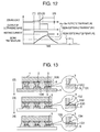
- a method wherein projection bumps, made of precious metal, each of which has a projection type shape are respectively formed on electrodes of a semiconductor chip; precious metal is formed on the surfaces of internal connection terminals of a printed circuit board; a thermosetting resin sheet which has been semi-cured by mixing therewith fine inorganic fillers is attached to a predetermined position of the printed circuit board; the printed circuit board is set on a heat stage; the chip is mounted thereto in a face down manner with the bumps and the internal connection terminals aligned with each other; a heated joining tool for applying the ultrasonic wave and the load is pressed against the chip from the upper side by a predetermined force; and after the precious metal bumps have been buried in the resin sheet, which was softened by the heating, to come into contact with the connection pads, respectively, the precious metal bumps are crushed to be metallically joined to the pads, respectively, while pushing out a part of the resin sheet from the part between the chip and the board to the outside by applying thereto the
- the bonding is carried out while pushing out a part of resin from the part between the chip and the board, the generation of the voids each having a size equal to or larger than the space defined between the chip and the board can be prevented with the probability of 100 %. Further, if even when the filler containing rate is high, this rate falls within the range in which the sheet can be produced, the space defined between the chip and the board is filled with the fillers with the fillers uniformly dispersed in that space. Thus, the assembly in which the filling quality of organic resin is fixed becomes possible.
- the reason that the high temperature reliability of the joining parts can be enhanced is that in the ultrasonic wave flip chip joining process, low-melting metal or an eutectic alloy which has been melted can be exhausted from the composition interfaces to provide the structure in which the joining is carried out using only high-melting point metal or a high-melting point alloy.
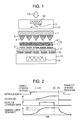
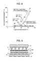
- Fig. 1 shows the construction of joining members and the periphery of the joining members in assembling a flip chip using the ultrasonic wave according to the present invention.
- Au bumps 3 are respectively formed on electrodes 2 of a semiconductor chip 1.
- the Au bumps are formed by utilizing the ball bonding method. Each of them has two-steps projection type shape in which the height there of is increased as the position thereon is nearer the center of the bump and is formed in such a way that the diameter is 100 ⁇ m, the head height is 100 ⁇ m, the shoulder height of the first step (on the side of the semiconductor chip 1) is 30 ⁇ m and the diameter of the second step (on the side of an organic printed circuit board 4) is 40 ⁇ m.
- connection terminals 5 containing Cu as the basic constituent have been plated with Ni, an Au plated film with 0.7 ⁇ m thickness is formed thereon.
- External connection terminals 9 for the connection to other chip, substrate or the like are formed on the rear face of the organic printed circuit board 4.
- the mean particle size is about 2 ⁇ m and the maximum value thereof is set equal to or smaller than 7 ⁇ m.
- the sheet thickness at this time is set to 50 ⁇ m which is about 1.2 times as large as the final bump height.
- the flip chip assembly structure of the present invention includes the semiconductor chip having a circuit for processing the electrical signals, and the semiconductor chip is provided with the electrodes on which the bumps are in turn formed, respectively.
- the internal connection terminals through which the electrical signal is fetched from the associated ones of the electrodes via the associated ones of the bumps are provided on the printed circuit board.
- the semi-cured resin sheet which is softened by the heating is inserted into the space defined between the semiconductor chip and the printed circuit board, the load is applied thereto, the heating is carried out therefor and the ultrasonic wave vibration is applied thereto, whereby the above-mentioned bumps and the above-mentioned internal connection terminals are metallically joined to each other.
- each of the bumps is made of precious metal, e.g., Au.
- Fig. 2 shows a time chart useful in explaining the joining process
- Fig. 3 shows cross sectional views showing the structure of the joining part at respective time points in the time chart shown in Fig. 2.
- the works are laminated and loaded on the heat stage, which is heated at a temperature of 150 degrees, while aligning these works with the heat stage, and then immediately, the joining tool which is being heated at 150 degrees is made descend to apply a light weight to the chip.
- the value of the load is set to 15 g/bump.
- the situation of the joining part at a time point (1) is shown in a part (1) of Fig. 3. Since the resin sheet 8 is still in the solid state, the Au bumps 3 are in the state of getting on the resin sheet 8. Referring back to Fig.
- the load is increased up to 100 g/bump while applying the ultrasonic wave vibration to the joining tool to join metallically the Au bumps 3 to the internal connection terminals 5 which were plated with Au. Since the resin sheet contains the less volatile components and also a part of the resin sheet is exhausted from the interfaces between the internal connection terminals 5 and the Au bumps 3 when the temperature is low before the progress of the bonding, the organic contamination of the surfaces to be joined due to the resin sheet 8 does not become so heavy as to impede the joining property. For this reason, the metallic joining at the level of obtaining the excellent electrical condition is achieved.
- the softening temperature of the resin sheet is the important factor in relation to the joining temperature.
- the proper range of the softening temperature in the present invention is desirably equal to or lower than 200 degrees from a viewpoint of not increasing the joining temperature, and while not in the strict sense of the words, is desirably equal to or higher than 70 degrees from the fact that in the joining process, the temperature needs to reach the softening temperature after having applied the pressure thereto.
- the resin sheet at 100 degrees is employed.
- the vibration amplitude of the ultrasonic wave is desirable in the range of 1 to 6 ⁇ m at the head of the joining tool. In the present embodiment, the vibration amplitude of the ultrasonic wave us set to 3 ⁇ m. Also, the time period for which the ultrasonic wave is being applied is desirable in the range of 50 to 500 ms.
- the present embodiment it is set to 300 ms.
- the load which is applied by the joining tool is held for a time period when the application of the ultrasonic wave is stopped to cure temporarily the resin (about 5 seconds in the present embodiment) and then is released. Thereafter, the works are moved from the ultrasonic wave joining position. On the other hand, the heating is continued to be maintained for 30 minutes to cure perfectly the resin and then the works are cooled down to the room temperature.
- the state of the joining part at a time point (4) when the load is released is shown in a part (3) of Fig. 3.
- the heads of the Au bumps 3 are crushed to be respectively joined to the internal connection terminals 5.
- the Au bumps 3 are partially metallically joined to the composition interfaces 16 in the state in which the resin 6 and the fillers 7 do not lie therebetween.
- the joining conditions are selected in such a way that the space defined between the chip 1 and the printed circuit board 4 becomes 40 + 15 ⁇ m when the initial bump size is the value shown in Fig. 1.
- the diameter in the first step on the chip side is 100 ⁇ m which is equal to the initial value, and the diameter in the second step on the board side is increased up to 50 ⁇ m because of the crushing.
- the two-steps shape is still left as it is.
- the space defined between the chip and the board is filled with a under fill 8', which contains, as the basic constituent, epoxy resin 26 containing a silica filler 27 with 2 ⁇ m mean particle size, in the void free state.
- a under fill 8' which contains, as the basic constituent, epoxy resin 26 containing a silica filler 27 with 2 ⁇ m mean particle size, in the void free state.
- the electrodes of the semiconductor chip are arranged in the periphery of the semiconductor chip or are arranged in the area-like pattern on the whole surface of the semiconductor chip, in any case, the same cross sectional structure is obtained. But, the wiring pattern of the board differs greatly therebetween due to the relation of the arrangement to the external connection terminals on the rear face of the board.
- the minimum size of the board can be made the same as that of the semiconductor chip.
- SiO 2 particles are employed for the inorganic fillers, alternatively, Al 2 O 3 particles or other insulating particles may also be employed.
- the conventional ultrasonic joining machine for assembling semiconductor chips does not have the machine which is capable of heating the horn of the ultrasonic wave oscillation system and the joining tool and also does not have the machine which is capable of joining the semiconductor chips using the ultrasonic wave by applying the heavy load exceeding 5 kg.
- the causes that the ultrasonic wave horn of the ultrasonic wave oscillation system and the joining tool can not be heated by the conventional machine are due to the following reasons.
- the reason that the conventional machine does not have the machine which is capable of joining the semiconductor chips using the ultrasonic wave by applying the heavy load is that it is difficult from the following reasons to design the construction of the vibration system for oscillating stably under the heavy load condition:
- a ultrasonic wave oscillating mechanism which has a heating function and has a special horn shape, and at the same time, by reducing the ultrasonic wave frequency from the conventional 60 kHz to 50 kHz, has developed a joining machine which is capable of oscillating stably the ultrasonic wave under the condition of the high temperature heating and the application of the heavy load.
- this joining machine will hereinbelow be described.
- the bumps which are formed on the chip are greatly deformed to absorb the warpage of the board and the dispersion of the bump heights to join reliably all of the points.
- the joining tool needs to have the construction in which it can descend while holding the balancing. Then, in the machine of the present embodiment, there is adopted the construction in which the strength member taking charge of the load shows a symmetry between the left and right halves, and the pressure application driving system and the central axis of the joining tool for pushing the joining member are arranged on the symmetrical axis. As a result, even when the joining load is increased, the surface of the joining tool can hold the balancing at all times.
- the description will hereinbelow be given with respect to the construction for heating the joining tool. Since the joining tool itself for applying the ultrasonic wave vibration and the load to the works has the small volume and hence has the small thermal capacity, it is easy to suffer the thermal fluctuation of the works. Therefore, the structure in which the main body of the ultrasonic wave horn having the large volume is heated is adopted to ensure the stability of the temperature, and in order to prevent the thermal damage of the ultrasonic wave vibrator, a radiating component which is excellent in the ultrasonic wave transmission characteristics is inserted between the ultrasonic wave vibrator and the ultrasonic wave horn. while there is the possibility that the transmission loss of the ultrasonic wave is increased to fluctuate, the vibrator is made oscillate with the input to the vibrator made large to compensate for the increase of the transmission loss and to reduce the influence of the fluctuation.
- the ultrasonic wave horns which are different in size for the joining temperatures are prepared.
- the temperature range which can be covered by one ultrasonic wave horn, while being different in the ultrasonic wave frequency and the horn shape, is set to ⁇ 30 degrees in the present embodiment.
- the ultrasonic wave horn which can oscillate stably under the heavy load.
- the ultrasonic wave horn in order to maintain the balancing of the joining tool, is processed into the shape which shows a symmetry between the left and right halves, and is held to the load application member at the left and right node points. For this reason, the horn is supported at the both ends thereof and hence suffers the bending deformation of the edge of the central load. If the rigidity of the horn is low, then the amount of bending deformation becomes large, and the horn shows an a symmetry between the upper and lower halves to generate the vibration modes other than the axial direction of the horn.
- the cross section of the horn is vertically divided by the effect of the slit(s), the substantial cross section in the direction along which the vibration is transmitted becomes small so that the vibration modes can be simplified and also the deformation can be suppressed due to the large thickness of the horn which has an influence on the flexural rigidity, which enables the oscillation of the ultrasonic wave to be stably carried out.
- the frequency of the ultrasonic wave is reduced from the conventional 60 kHz to 50 kHz so that the coefficient of fluctuation in the resonance point is reduced against the change in the temperature and the strain of the horn, thereby realizing the stable oscillation of the ultrasonic wave.
- Fig. 4 shows the joining machine which is employed in the present embodiment.
- the machine body includes: a supporting frame 41; a supporting chassis 42; a pressure applying mechanism 43; a mechanism 44 for heating a chip and for oscillating a ultrasonic wave; a board heating mechanism 46; an alignment driving mechanism 45; a work observing mechanism 47; a board carrying mechanism 49; and a chip carrying mechanism 48.
- the work observation mechanism 47 has the function of taking in the vertical image through an optical mechanism inserted into the space defined between the printed circuit board 4 and the semiconductor chip 1 to detect the positional misalignment. On the basis of this information, the adjustment is carried out in the position alignment driving mechanism.
- Fig. 5 shows the detailed construction of the machine shown in Fig. 4.
- the pressure applying mechanism 43 adopts the serve motor driving system for detecting an output from a pressure sensor 50 to adjust automatically the current value to the setting value.
- a ultrasonic wave vibrator 51 is coupled to a ultrasonic wave horn 55 through a vibration amplifying component 54 having a radiating component 52 and a flange mechanism 53.
- the ultrasonic wave horn 55 is formed integrally with a joining tool 56.
- the heaters 12 are mounted to the ultrasonic wave horn 55 in the positions which are located at the vertical centers and which shows a symmetry between the left and right halves.
- the device is carried out in such a way that through holes (slits) are provided in the positions which shows a point symmetry with respect to the center of the ultrasonic wave horn 55 and hence the vibration mode within the horn becomes a single mode corresponding to only one axial direction.
- a suction hole 57 for sucking the works
- a super-hard member 58 is joined to the tip of the joining tool in order to lengthen the life thereof.
- the ultrasonic wave vibrating mechanism is mounted to a member 59 for supporting the vibration system through a flange which is mounted to the node position of the vibration.
- the positional misalignment judging mechanism includes an optical head 512 consisting of a half mirror 510 and a CCD sensor 511, and a processing circuit 513 for judging the positional misalignment on the basis of the image processing.
- the information from the optical head 512 is transmitted to the processing circuit 513 through a cable 514.
- the optical head 512 includes a movable mechanism and serves to make a round trip between the joining position and the stand-by position every sample.
- the device is applied to the shape of the ultrasonic wave horn, whereby the vibration mode of the ultrasonic wave horn having the high rigidity can be controlled in such a way as to be made a single mode corresponding to only one axis.
- the load applying construction of the vibration system is made the two-points support by the flange mechanism 53, and the shape is made show a symmetry between the left and right halves for the point of application of the force of the joining tool, whereby even if the heavy load is applied to deform the vibration system, the balancing of the tool surface can be held.
- the precious metal bumps of the multipin LSI chip can be reliably metallically joined to the precious metal pads of the board under the low temperature condition by utilizing the ultrasonic wave energy.
- the present joining machine has preferably a mechanism for supplying an organic tape between the joining tool and the work.
- an organic tape 60 made of polyimide is arranged at the head of the joining tool 56 which is formed integrally with the ultrasonic wave horn 55.
- the organic tape is successively forwarded from the side of a roll 61 by take-up mechanisms 62 and 63.
- a new tape is supplied to the position under the tool every joining.
- Holes 64 for sucking the work are provided in the organic tape and the tape forwarding position is controlled in such a way that the hole is aligned with the suction hole of the tool.
- the organic tape may be either thermoplastic or thermosetting
- the high rigidity is required therefor in such a way that the absorption of the ultrasonic wave becomes less
- the elastic modulus is desirable in the range of 1 to 100 GPa.
- the elastic modulus of polyimide is about 9 GPa.
- Fig. 7 shows an example of an enlarged photograph of the bump joining part.
- the under fill resin is filled without any of defects and the bumps and the pads are metallically joined to each other though the void defects are present.
- the precious metal bumps and the precious metal pads on the board side are metallically joined to each other, whereby with respect to the electrical resistance of the connection part, the contact resistance of the composition interface can be greatly reduced.
- the resistance value is in the range of several tens to one hundred and several tens m ⁇ , whereas in the structure according to the present invention, it becomes clear that the resistance can be reduced to the range of 0.1 to 10 m ⁇ .
- the present invention since there is adopted the method wherein in the state of laminating the board, the resin sheet and the chip, the heat and the ultrasonic wave vibration are applied to carry out the compression joining, the Au bumps push the softened resin away to come into contact with the Au pads on the board, respectively, and in addition thereto, the metallic joining between the bumps and the internal connection terminals is achieved by the ultrasonic wave vibration.
- the flip chip assembly for the semiconductor chip including the metallic joining between the Au bumps and the Au pads, and the resin filling into the space defined between the chip and the board can be carried out in one process to enhance the productivity, the electrical resistance of the connection part can be reduced since the metallic joining between the Au bumps and the Au pads is achieved, and the assembly reliability can be enhanced since the under fill filling which is void free is possible using the resin having the high filler containing rate.
- the flip chip assembly method which is excellent in the productivity, the electrical characteristics and the reliability.
- the under fill can be formed in a void free manner, whereby the peeling-off of the joining part in the reflow due to the vaporization expansion of the moisture in the voids can be prevented from being generated.
- the chip and the board are firmly bonded with the under fill in which the filler containing rate is increased and the coefficient of thermal expansion thereof is made smaller than 20 x 10 -6 /degree which is equal to that of the board, whereby the thermal strain which is caused along with the temperature change can be equally dispersed among the chip, the bumps and the board to lengthen the temperature cycle life.
- the Au/Au joining is metallically stable under the high temperatures, it is possible to provide the assembly structure which is excellent in the high temperature life.
- the thermal expansion coefficient of the under fill is preferably in the range of 10 to 25 x 10 -6 /degree.
- Fig. 8 shows the generation rate of the voids in the under fill in the semiconductor assembly products which are manufactured in accordance with the method shown in Figs. 1, 2 and 3.
- the results in the conventional system of injecting the liquid resin after completion of the joining are plotted.
- the filler containing amount is increased, then the fluidity is reduced.
- the void generation rate is increased as the space defined between the chip and the board is smaller and the chip size is larger.
- the filler containing amount exceeds 50 %, then it becomes difficult to remove the voids.
- the generation of the voids when supplying the resin from one side is the problem which arises due to the fact that the speed of the penetration of the resin by the capillary phenomenon differs depending on the places due to the presence of the bumps, and is caused by the entrainment of air. For this reason, the voids which have the size corresponding to the space defined between the chip and the board are present.
- the gases which are present in the space defined between the chip and the resin sheet and the space between the board and the resin sheet are exhausted to the outside by the pressure, and further the resin flows in the direction of being pushed out from the inside to the outside to exhaust the gases.
- the generation rate of large voids becomes zero. If the gases should remain in both of the spaces, the volume thereof is very small. Thus, this does not become the problem such as the occurrence of the reflow cracks resulting from the reduction of the strength or the moisture absorption. That is, the occurrence of the failure due to the void defects can be avoided perfectly.
- the resin having the filler containing rate of 50 vol% or more is formed between the chip and the board in the void free manner to be bonded thereto and to be cured, whereby in the conduction of the temperature equal to or lower than the curing temperature of the resin, the compressive force is applied to the Au bump joining parts at all times by the contraction of the resin. Therefore, the life up to which the assembly product is brought to the disconnection failure when subjecting the assembly products to the temperature cycling test can be greatly lengthened.
- the filler containing rate of the resin can be made high, the coefficient of thermal expansion thereof can be made equal to that of Au.
- the fluctuation of the filler distribution in the resin can be made small, the stress which is generated in the Au bumps or the resin when being applied to the temperature cycle does not fluctuate, which results in the life up to which the assembly product is brought to the disconnection failure being able to be greatly lengthened.
- the thickness of the semiconductor chip is 50 ⁇ m
- the printed circuit board is the polyimide film with 25 ⁇ m thickness
- the thickness of the wiring Cu foil is 3 ⁇ m
- the size of the bump shape is so large as to be 100 ⁇ m on the chip side and is so small as to be 40 ⁇ m in the second step, and the joining of the bumps to the pads on the board is carried out in the second step, the stress (the yield stress of Au x the joining area on the board side/the joining area on the chip side) which is applied to the chip side during the bonding can be reduced to the small value which is about one over several number of the yield strength of Au. For this reason, there is offered the effect that the chip damage under the electrodes in the flip chip assembly process can be reduced to enhance the assembly yield.
- the liquid epoxy resin with about 50 ⁇ m thickness containing the insulating inorganic fillers (SiO 2 : the mean particle size is 1 ⁇ m, and the maximum value is 7 ⁇ m) is applied to the chip mounting area of the board, and thereafter immediately, the chip with the Au bumps is mounted on the liquid resin to carry out the ultrasonic wave joining, and subsequently, the curing processing at 150 degrees for 30 minutes is carried out.
- the liquid resin while the pad surfaces of the board are contaminated with the resin, the joining condition is made the condition of the heavy load or the high ultrasonic wave power, whereby it is confirmed that the partial metallic joining can be achieved.
- other thermosetting resin such as the phenol resin may also be employed.
- the same effects as those of the first embodiment can be offered.
- the supply of the resin becomes easy because the printing system can be adopted, there is offered the effect that the productivity can be enhanced.
- the manday of production is less as compared with the case where the liquid sheet is employed, there is the advantage that the cost of the material is low and hence the low cost of the assembly products can be realized.
- Fig. 9 shows an embodiment of the flip chip assembly method according to the present invention.
- the Au bumps 3 are respectively formed on the electrodes (the Al electrodes) 2 of the chip 1 by utilizing the ball bonding method.
- the initial bump diameter is 60 ⁇ m
- the diameter in the second step is 35 ⁇ m
- the bump height is 80 ⁇ m
- the shoulder height in the first step is 10 ⁇ m.
- Two sheets of resin sheets are employed.
- An Au film with 0.5 ⁇ m thickness is formed on the most upper surfaces of the internal connection terminals 5 of the board 4. The joining process after having carried out the lamination in the arrangement shown in the figure is the same as that of the first embodiment.
- Fig. 10 is an enlarged view of the cross sectional structure of the joining part after having joined the elements shown in Fig. 9.
- a under fill 8' includes a low thermal expansion layer 92 in which the fillers are filled with high density, and an intermediate thermal expansion layer 93 having the lower filler density, and the interface therebetween becomes the integrated structure through the inclined region in which the filler filling rate is continuously changed.
- the coefficient of thermal expansion of the resin in the part near the board is higher than that in the part near the chip.
- the containing rate of the inorganic fillers contained in the resin in the part near the board is lower than that in the part near the chip.
- the joining part on the chip side is wide, the column made of Au which is smaller than the joining part is built thereon, and the head of the column is joined to the associated one of the internal connection terminals.
- the sate in which the metallic joining is achieved in at least a part of the contact surface is provided.
- Fig. 11 shows the Weibull plot of the failure occurrence rate when the samples having the different filler containing amounts are subjected to the temperature cycling test. Since the under fill resin has the high thermal expansion coefficient, it is short-lived in the state in which there is no filler. When the filler material which has the lower thermal expansion coefficient than that of the under fill resin gets mixed therewith to decrease the thermal expansion, the life is lengthened. In this case, when employing the under fill resin having the filler containing rate of 50 % or the two-layers under fill, there is shown the life exceeding 1,000 cycles.
- the method wherein the under fill having the filler containing rate of 70 % or more can be filled in a void free manner is only the method according to the present invention. Thus, it is said that the two-layers system is not the possible structure until the method of the present invention has been made. That is, it is possible to provide the highly reliable flip chip assembly products by the embodiment of the present invention.
- the under fill is divided into the two layers in such a way that the low thermal expansion resin sheet is arranged on the chip side in correspondence to Si, while the intermediate thermal expansion resin sheet is arranged on the board side in correspondence to the resin board, the coefficient of thermal expansion between the chip and the under fill and the coefficient of thermal expansion between the board and the under fill are near each other so that the generation of the shearing stress resulting from the thermal strain in both of the interfaces is reduced.
- the thermal stress which is generated in the joining part between the chip and the bumps as well as in the joining part between the board and the bumps can be reduced, the peeling-off between the chip and the under fill as well as between the board and the under fill can be prevented from being generated, and the peeling-off disconnection in the composition interfaces of the Au bumps can be prevented.
- the assembly reliability can be remarkably enhanced.
- the thermal expansion coefficient is continuously changed due to the inclination structure. Therefore, since the wide area in the central part of each of the Au bumps suffers the thermal strain, the local stress concentration is not generated. Further, since the Au bump part of the bulk suffers the stress, the reliability can be made far higher than that in the structure in which the composition interface suffers the stress.
- the materials of the bumps and the internal connection terminal surfaces of the printed circuit board in the first embodiment there are selected Ag which is readily separated from oxygen at the temperature of 20 degrees or higher though it is slightly oxidized in the atmosphere, and Pd and Pt each of which forms hardly the oxide film in the temperature region ranging from the room temperature to the joining temperature of 200 degrees though it is oxidized at the high temperatures.
- the resin agent for the under fill only the composite resin of the polyimide resin and the epoxy resin is selected.
- the joining is implemented under the condition in which the frequency is 50 kHz, and the chip amplitude is 1 ⁇ m (the tool amplitude is 3 ⁇ m).
- connection resistance can be reduced to the range of 0.1 to 10 m ⁇ .
- Fig. 12 shows a time chart of the joining conditions in the case where the low-melting point metal (an Sn film) which reacts on the Au bumps to be melted at 217 degrees by the eutectic reaction is formed on the internal connection terminals on the printed circuit board side to carry out the flip chip joining. While the base element structure in the assembly is completely the same as that in Fig. 1, points of difference therefrom are that the heating is carried out only from the joining tool side, and that the material of the pads is changed from Au to Sn. In Fig. 12, after having applied the load to the works, the joining tool is heated in an instant by the pulse heater, and the works are heated from the chip side.
- the low-melting point metal an Sn film
- the ultrasonic wave is applied to the works through the joining tool while increasing the load applied to the works.
- the heating is continuously carried out until the work temperature exceeds the Au-Sn eutectic temperature (217 degrees) to reach 235 degrees.
- the time period when applying the ultrasonic wave is set in such a way that the ultrasonic wave is applied for a predetermined time after the work temperature has reached the Au-Sn eutectic temperature.
- the ultrasonic wave is applied for 150 ms. The application of the ultrasonic wave is stopped and roughly at the same time, the heating by the pulse heater is stopped.
- the load is released, and the works are taken out from the joining machine. Thereafter, the baking processing is carried out at 180 degrees for 10 minutes in the heating system such as the constant temperature oven to cure perfectly the resin.
- Fig. 13 shows a schematic view of cross sections of the joining part at time points (2), (3) and (4) shown in the time chart of Fig. 12.
- the projecting An bumps 3 are pushed into the resin sheet 8 along with the softening of the resin, and if the thickness of the resin film is suitably selected, then there is obtained the state in which the bumps 3 come into contact with the pads 131, respectively.
- the load is supported by the Au bumps and the surfaces 130 plated with Sn and in the solid phase.
- the Au-Sn eutectic reaction occurs in the region in which Au and Sn are adhered closely to each other so that the melting liquid 132 starts to be formed while Sn underlying the bumps is mechanically pushed out to the outside by the vibration friction of the Au bumps 3.
- the Au bumps 3 are joined to the internal connection terminals (the Cu pads) 5 through an AuSn layer 135 which is rich in Au and a CuSn layer 133.
- An Au-Sn eutectic alloy having a low melting point which was formed in the joining process is pushed out to the peripheries of the bumps to form fillets 134.
- the film plated with Sn which is located outside the bumps is melted one time in the stage in which it is heated at 232 degrees, but reacts on the underlying Cu to form CuSn compound 133 which has a high melting point and is isothermally solidified.
- the assembly method having the high productivity can be provided similarly to the first embodiment.
- the process in which the melted layer is formed in the composition interface one time to carry out the joining is adopted. Therefore, the occurrence of the joining failure due to the organic contamination or the like of the composition surface can be reduced, the joining can be carried out under the joining conditions of the light load and the low ultrasonic wave power, and the occurrence of the chip damage can be reduced.
- the assembly method having a high yield.
- the low-melting point alloy which is formed in the composition interface is exhausted to the outside of the bumps by the application of the load and the ultrasonic wave vibration, the alloy containing Sn which is left in the composition interface at a time point of completion of the joining is only the alloy having a high melting point, and hence the melting point of metal constituting the joining part can be made equal to or higher than 275 degrees. Since the heating temperature in the soldering assembly is equal to or lower than 250 degrees, even if that alloy is heated in the soldering assembly to the printed circuit board or the like, it is not remelted. Thus, that alloy is also excellent in the high temperature heat resistance, and hence there is no problem in the heat resistance of the joining parts.
- the assembly reliability can be enhanced.
- the assembly structure of the present embodiment similarly to the first embodiment of Fig. 1, since the package can be thinned, and also the package can be miniaturized to the size equal to that of the chip, the ultrathin and small semiconductor package can be provided.
- the joining temperature is set to 180 degrees in In, 150 degrees in Ga and 150 degrees in Tl, and other joining conditions are made the same as those of the fifth embodiment.
- the low-melting point layer can be exhausted from the composition interface to the outside by the application of the load and the ultrasonic wave vibration, and hence the joining part having a high melting point can be obtained similarly to the case where Sn is employed.
- the heat resistance of the joining part after completion of the joining can be enhanced, the same effects as those of the fifth embodiment can be offered.
- the joining temperature can be reduced to a level equal to or lower than 200 degrees, the thermal stress which is generated in the cooling process after completion of the joining can be reduced, and the chip damage in the assembly process can be reduced.
- the assembly yield can be enhanced.
- the low-melting point metal material may be employed as long as it is constituted by metal or an alloy which has a melting temperature equal to or lower than 250 degrees or in which a melting temperature is equal to or lower than 250 degrees when alloyed with the precious metal bumps.
- Fig. 14 shows another embodiment of the heating system for the ultrasonic wave horn.
- an electrical conducting ceramic plate i.e., a heater chip 140 is joined to the head of the joining tool which is integrated with the ultrasonic wave horn 55, and a mechanism 141 for supplying a current to the heater chip 140 is provided therefor.
- a current pulse is supplied to the heater chip every joining to carry out the instantaneous heating. While since the heater chip has the small heat capacity, it is heated to a high temperature during the supply of the current pulse, the supply of the current pulse is stopped, whereby the temperature of the heater chip is reduced for a short time period. This is the feature in the heater chip.
- the joining materials are the materials such as the precious metal bumps and the Sn plated pads
- the heating can be stopped while applying the pressure to carry out the cooling for a short time period. Therefore, the joining part having the excellent heat resistance can be obtained by employing the low-melting point metal, and at the same time, the damage of the joining parts due to the thermal contraction in the cooling process can be prevented.
- the highly reliable joining can be carried out without injuring the productivity in the mass production line.
- Fig. 15 shows an embodiment of the precious metal bump shape which is suitable for the flip chip assembly of the present invention.
- a part (a) of Fig. 15 shows the case of the stud bumps.
- the Au stud bumps 3 are respectively formed on the electrodes (the Al electrodes) 2 of the semiconductor chip (the Si chip) 1 by utilizing the ball bonding method.
- the initial ball size, the capillary size and the joining conditions are selected in such a way that with respect to the Au stud bump shape, the ratio of the diameter 150 at the joining crushed height level of the bump upper part to the diameter 151 of the joining part between the Au bumps and the Al electrodes becomes in the range of 1/2 to 1/3 in the area ratio.
- the diameter of the composition surface on the chip side can be set to the range of 80 to 90 ⁇ m and also the diameter of the bonding surface on the board side can be set to the range of 40 to 45 ⁇ m.
- a part (b) of Fig. 15 shows the case of the two-step plated bumps.
- the diameter ratio is selected in such a way that the area ratio of the second step to the first step becomes in the range of 1/2 to 1/3 or less.
- a part (c) of Fig. 15 shows the case of the plated bumps each of which is of the shape having the sharp head. In this case, the shape is controlled in such a way that the area ratio of the joining crushed height position to the base of the bump becomes in the range of 1/2 to 1/3 or less.
- reference numeral 136 designates a passivation film.
- reference numerals 152 and 153 designates a diameter of a upper part and a diameter of a lower part, respectively.
- Fig. 16 shows the cross sectional structure of the flip chip assembly part when the plated bumps shown in a part (b) of Fig. 15 are employed.
- the area of the interface of the bump/the barrier metal/the Al electrode is about 0.0036 mm 2
- the joining area of the bump/the Au plated land of the board is about 0.00081 mm 2 .
- the joining area of the latter is made so small as to be about 23 % of the joining area of the former.
- the whole plated bump 3 of the figure is made of Au
- the bumps in each of which the first step is formed of Cu metal plating and the second step is formed of Au metal plating, and their heights are respectively 10 ⁇ m and 20 ⁇ m are manufactured by way of trial.
- reference numeral 160 designates Au metal plating.
- Fig. 17 shows the cross sectional structure of the flip chip assembly part when the Au bumps are respectively formed on the chip side and the board side.
- the size is adjusted in such a way that the ratio of the area of the transverse section of each of the Au plated bumps 3 on the chip side to the area of each of the joining parts becomes in the range of 2 to 3 or more.
- the bump size on the chip side is set to 60 ⁇ m square
- the bump size on the board side is set to 40 ⁇ m square.
- reference numeral 170 designates a plated resist film.
- each of the precious metal bumps is preferably selected in such a way that the joining area on the chip side becomes larger than that on the board side by 40 percent or more.
- the large shearing stress is generated in the chip board underlying the bumps to generate the chip damage.
- the value of the shearing stress which is applied to the chip side through the bumps becomes the value which is obtained by multiplying the yield strength of each of the Au bumps by the area ratio between the board side and the chip side, in the present invention, that value can be reduced to 70 percent or less of the yield strength of each of the Au bumps, and hence the occurrence of the damage can be greatly reduced.
- Fig. 18 shows the relationship between the SiO 2 filler containing amount and the void generation rate of the epoxy resin based under fill in the flip chip assembly when employing the Au plated bumps.
- the Au plated bumps since if the bump height is increased, then the cost is correspondingly increased that so much, the bumps each of which is as low as possible will be employed. The lowest height becomes the height at which the warpage of the board and the dispersion in the thickness thereof, and the dispersion in the pad height can be absorbed by the deformation of the bumps.
- the probability of generation of the voids each having the size of several tens ⁇ m or more becoming a problem can be made zero irrespective of the gap.
- Fig. 19 shows the relationship between the bump height and the disconnection failure occurrence rate in the temperature cycling test when the joining temperature and the presence and absence of the under fill are changed.
- the graph shows a tendency in which the disconnection failure is easy to occur as the height is lower, and also shows a tendency in which the permanent set is increased to increase the disconnection failure occurrence rate as the joining temperature is higher.
- Fig. 20 shows an example of the cross sectional structure of a BGA package to which the flip chip assembly structure according to the present invention is applied.
- the Au bumps 3 which have been formed by the tearing-off type of the ball bonding method are respectively loaded on the Al electrodes 2 which are arranged on the area of the semiconductor chip (the Si chip) 1.
- a film 200 of Ni with 5 ⁇ m thickness/Au with 0.5 m thickness is formed on the internal connection terminals (the Cu pattern) 5 each with 35 ⁇ m thickness in the positions corresponding to the Al electrodes of the chip on the chip side of the printed circuit board (the glass epoxy board) 4 by the electroless plating.
- the pads for the solder bumps (the external connection terminals) 9 each of which is made of the same material as that of the surface on the chip side are formed, and the solder ball bumps are loaded thereon. Since the Au plating of the pads dissolves into the solder when loading the solder, the Ni plated film and the solder are directly joined to each other in the state of completion of the package.
- the Au bumps on the chip and the Au plated pads on the board are electrically connected to each other through the metallic bonding by the thermal compression joining utilizing the ultrasonic wave, and the space defined between the chip and the board is filled with the under fill 8' containing the insulating inorganic filler 7 (SiO 2 particles) showing the low thermal expansion and the thermosetting resin (the epoxy resin) 6.
- the volume ratio of the epoxy resin to the SiO 2 particles is 1 : 2.
- the bump height is 60 ⁇ m, the diameter of the Au/Au joining part is 30 ⁇ m, and the diameter of the Al/Al joining part is 80 ⁇ m.
- the bump height is deformed from the initial value of 100 ⁇ m to 40 ⁇ m, and the wire part is crushed to the level equal to the second step shoulder which is formed in the hole of the capillary or up to the position which is slightly near the head.
- the joining since the joining is carried out at the head parts of the stud bumps, the joining can be carried out with the light load of several tens to several hundreds mN per bump, and even in the case of the multipin LSI chip having several thousands pins, the flip chip assembly can be carried out by the Au/Au metallic joining without generating any of the chip cracks.
- the bump height is increased and the chip and the board are firmly bonded to each other by the under fill showing the low thermal expansion, the strain which is applied to the joined bumps becomes very small. Also, since as another effect of the under fill resin, the strain is equally dispersed among the whole bumps, the temperature cycle reliability as the package can be remarkably enhanced.
- the mother board and the chip can be electrically connected with shortest distance, even when the high performance LSI in which the clock frequency of the chip exceeds several hundreds MHz is loaded, the assembly for the electronic apparatus becomes possible without injuring the performance thereof.
- the wiring distributed between the internal connection pads and the external connection pads the number of wirings distributed between the adjacent pads can be reduced by utilizing the through hole(s) as much as possible.
- the pitch of the external connection pads of the board can be shortened, which makes possible the miniaturization of the package size.
- the heat resistance of the internal connection parts is sufficiently higher than the refractory temperature of the resin, any of the problems does not arise at all in the solder reflow process in which the package is mounted to the printed circuit board.
- Fig. 21 shows an embodiment of the cross sectional structure of a tape BGA package to which the flip chip assembly structure according to the present invention is applied.
- the Au plated bumps 3 are respectively formed on the electrodes (the Al electrode pads) 2 of the semiconductor chip (the Si chip) 1.
- An opening part which is smaller than the pad formation area of the chips is provided at the center of the printed circuit board (the tape board) 4 containing, as the basic constituent, the polyimide film with 50 ⁇ m thickness, and a Cu wiring pattern 202 with 5 ⁇ m thickness is formed on one side.
- Each of the surfaces of the internal connection leads 210 has the Au plated layer with 0.5 ⁇ m thickness, and the solder ball bumps 201 are respectively formed on the pads (the external connection terminals) 9 for the solder bumps each of which is formed by providing the opening in the tape board.
- the stiffeners 211 are adhered through the adhesive agent 212 to the tape board of the area, in the periphery of the chip, in which the solder bumps are formed.
- the Au bumps and the internal connection leads of the chip are connected to each other through the Au/Au metallic joining, and the space defined between the tape and the chip is filled with the resin containing the spheroidal fillers each of which has the lower thermal expansion coefficient than that of the resin.
- Each of the Au bumps is of a square of 20 ⁇ m x 20 ⁇ m, and the Au bumps are joined under the condition in which the height after completion of the compression joining is 10 ⁇ m in the low position. Then, the assembly is carried out under the conditions in which the joining temperature is 100 degrees, the joining load is 50 mN/bump, and the vibration amplitude of the ultrasonic wave is 3 ⁇ m in the tool and 1.5 ⁇ m in the chip. Then, the assembly is carried out in the order of the chip joining + the under fill filling, the stiffener bonding, and the solder ball loading. In this case, since the under fill has the shape which is free from the generation of the voids, it may be led thereinto after completion of the joining.
- the slitting is formed in plural pins from the opening part, in the chip connection area of the tape board.
- the wiring pitch can be made the pitch of 30 ⁇ m, and hence the LSI chip having so narrow pad pitch as to be 30 ⁇ m can be flip-chip assembled.
- the joining temperature is so high as to be equal to or higher than 200 degrees (230 degrees in the Au-Sn eutectic joining)
- the strain due to the thermal expansion of the tape board and the thermal expansion of the Cu foil, and the position shift due to the thermal expansion difference to the chip become the problems.
- the joining temperature can be made drop to the room temperature, even in the connection having the fine pitch, the metallic joining can be made with high accuracy, and hence it is possible to provide the highly accurate and highly reliable flip chip assembly structure.
- the under fill resin showing the low thermal expansion is solidified for the connection parts and the opening is formed at the center of the tape board. Therefore, in the temperature fluctuation under the practical use environment, the thermal strain which is applied to the bump joining parts can be reduced by the fixing effect of the under fill and the effect of absorbing the strain by the slit(s), and hence the temperature cycle reliability of the package can be greatly improved.
- the heat resistance of the internal connection part is sufficiently higher than the refractory temperature of the resin, in the solder reflow process in which the package is mounted to the printed circuit board, there is no problem.
- Fig. 22 shows an embodiment of the package cross sectional structure when the flip chip assembly structure of the present invention is applied to the semiconductor package which is of a one side resin mold type.
- the Au stud bumps 3 are respectively formed on the Al electrodes 2 of the semiconductor chip (the LSI chip) 1.
- the wiring pattern and the internal connection pads are formed on the chip side of the printed circuit board (the organic carrier board) 4 containing the glass cloth and the epoxy resin.
- Each of the internal connection pads is constituted by each of the internal connection terminals (the Cu pads) 5 and the Ni/Au plating 200 formed thereon.
- the external connection terminals 9 are formed on the lower side of the board, and the solder bumps 201 are respectively formed on the external connection terminals 9.
- the metallic joining of Au/Au by the ultrasonic wave joining method of the present invention is achieved for the internal connection pads and the Au stud bumps.
- the gap defined between the chip and the board is filled with the first resin 220 containing the thermosetting resin 6 and the spheroidal insulating inorganic fillers 7 each of which shows the lower thermal expansion than that of the thermosetting resin 6 and has the size equal to or smaller than 1/3 of the above-mentioned gap.
- one side of the board is molded with second resin 223 containing grinding-shaped large filler particles 221 each showing the low thermal expansion and thermosetting resin 222 in such a way as for the chip to be covered.
- the large filler shape is not limited to the grinding type, and hence may be spheroidal or of other shape as long as the cost permits.
- the method wherein the process of joining the chip to the organic carrier board is carried out through the process of sandwiching therebetween the resin sheet to form the flip chip assembly. Therefore, the multipin batch joining and the under fill resin filling can be carried out at the same time, and also the voids which are easy to be generated in the gap defined between the chip and the board can be perfectly removed.
- the problems of the reduction of the productivity as compared with the wire bonding method, the reflow cracks due to the generation of the voids, and the like can be solved.
- the whole chip is molded, whereby the force of pressing the chip against the board becomes strong as compared with the structure of only the normal under fill encapsulation, and the compressive stress acts on the internal connection parts at all times.
- the problem that the cracks are generated in the joining parts due to the thermal strain in the temperature cycle or the like to bring the product to the disconnection can be prevented, and also it is possible to provide the package which has the very high reliability.
- the electrical characteristics are excellent, the heat resistance of the internal connection is high and hence there is no problem in terms of the mounting of the printed circuit board, and the package height can be reduced.
- Fig. 23 shows an embodiment in which the flip chip assembly structure of the present invention is applied to a ceramic module.
- Ag series thick film conductor patterns 230, 231 and 232 which were formed by the printing and the firing are formed on the printed circuit board (the ceramic substrate) 4.
- the Au stud bumps 3 are formed on the conductor pattern 230, which is flip-chip connected, by the ball bonding to be flattened by the leveling processing.
- Passive components 233 and 234, and the conductors on the ceramic substrate are electrically connected to each other through the Sn series solder 235 and 236.
- the Au stud bumps 3' are formed on the Al electrodes 2 of the semiconductor chip (the bare chip) 1 by utilizing the tearing-off method and are metallically joined to the flattened Au stud bump surfaces of the ceramic substrate through the Au-Au metallic joining. Right before carrying out the joining process, the surfaces of the flattened Au stud bumps are cleaned by utilizing the sputtering cleaning method in order to carry out the assembly.
- the space defined between the chip of the module and the substrate is filled with the thermosetting under fill resin 8' containing 70 % or more SiO 2 fillers each showing the low thermal expansion.
- the flattened bump size on the substrate side is 15 ⁇ m (thickness) x 80 ⁇ m (diameter), and the bump size on the chip side is 80 ⁇ m (height) x 60 ⁇ m (diameter) in the initial values and that bump size after completion of the compression joining is 40 ⁇ m (height) x 60 ⁇ m (diameter).
- the parts which are crushed by the joining are up to the wire part and the upper part in the second step which is formed by the capillary hole, and the base part in the first step which is formed as the result of crushing the initial ball is hardly deformed.
- the joining is carried out under these joining conditions.
- the LSI connection pad pitch can be reduced from 300 ⁇ m or more level to 100 to 200 ⁇ m level, and hence the LSI chip which is manufactured for the normal wire bonding mounting can be applied to the flip chip assembly as it is.
- the solder for C4 is the high-melting point solder, there is the problem that the assembly is difficult to be carried out in the lead (Pb) free manner, which becomes a problem in terms of the environmental pollution.
- Fig. 24 shows an embodiment of the procedure of assembling the various modules.
- the module board in which the chip connection pads are plated with Au, the LSI chip having the Au bumps formed thereon, and the semi-cured organic film or the liquid resin.
- the organic film the module board, the organic film and the LSI chip are laminated with the positions of their connection terminals aligned with each other to be loaded, and then the Au bumps break through the softened organic film to be metallically joined to the Au pads, respectively, by applying thereto the pressure, the heat and the ultrasonic wave.
- the heating is held to cure the resin, and the solder paste printing is carried out to load thereon the component to be soldered, and the reflow processing is carried out to perform the soldering.
- the liquid under fill resin in the case where the liquid under fill resin is used, in the joining process, only the board and the chip are aligned with each other to carry out the flip chip joining first of all, and thereafter, the liquid resin is injected into the space defined between the board and the chip by the capillary phenomenon or the application of the pressure to carry out the curing processing.
- the assembly is carried out on the basis of such a procedure.
- Fig. 25 shows another embodiment of the procedure of assembling the ceramic module which is reverse to Fig. 24.
- the same members as those in Fig. 24 are prepared.
- the components to be soldered are loaded on the module board through the printing and reflow process. Since in this process, the conductor pattern of the board is contaminated by the organic vapor such as flux or the diffusion to the surface of the underlying material(s), after having loaded the components to be soldered, the cleaning by the organic agent and the cleaning processing by the sputtering cleaning are carried out. Thereafter, the organic paste containing the fillers is applied onto the board and the chip having the Au bumps formed thereon is positioned to be loaded, and then is joined thereto by the application of the heating and the pressure utilizing the ultrasonic wave. Finally, the semi-cured organic resin is perfectly cured to complete the assembly.
- Fig. 26 shows an embodiment of the cross sectional structure of a multichip module employing an organic board according to the present invention.
- a rewiring layer 253 is formed on the surfaces of LSI chips 250 and 251, and the chip electrodes 2 which are arranged in the periphery are rearranged on the whole surfaces of the chips. While each of the chip electrodes is made of an Al alloy, each of rearranged electrodes 254 is made of the material in which the core is made of Cu and the most upper surface is made of Au.
- the Au bumps 3 are respectively formed on the rearranged electrodes by utilizing the ball bonding method or the plating method.
- the organic printed circuit board (the organic module board) 4 is made of glass epoxy resin, and the internal connection terminals 5 are formed on the face thereof on the chip side, while the external connection terminals 9 are formed on the face thereof on the opposite side. Sn based solder bumps 201 are respectively formed on the external connection terminals.
- Each of the internal connection terminals has the structure in which the Cu core is plated with Au, and the Au bumps of the chip are metallically joined thereto.
- the space defined between the chip and the board is filled with the thermosetting under fill resin 8' containing the minute spheroidal fillers each having the lower thermal expansion coefficient than that of the resin.
- the gap between the chip and the chip is filled with the under fill resin in the form of the organic film, whereby even for the narrow gap of about 1 mm, the under fill resin is cut off.
- the plane distribution of the minute spheroidal fillers contained in the under fill resin is controlled in such a way that the dispersion in the containing rate when obtaining the filler containing rate of 1 mm square size from an arbitrary place is equal to or smaller than ⁇ 5 % at a maximum. This can be realized only by the method wherein the under fill resin is supplied in the form of the sheet in which the fillers are uniformly dispersed.
- the pitch and the arrangement of the electrodes can be selected irrespective of the pitch and the arrangement of the initial chip electrodes, and hence no matter what kind of a specification the chip of interest has, it can be loaded on the module board. Therefore, if the connection electrodes are concentratedly arranged in the center of the chip, then the distance between the farthest bumps is shortened. As a result, the maximum thermal deformation which is generated in proportion to that distance can be reduced, and hence the thermal fatigue life can be greatly lengthened. In addition, if the connection electrodes are dispersed into the whole surface of the chip, then the electrode pitch can be roughed.
- the manufacture of the module board may be of low accuracy, there is the advantage that the low cost can be realized.
- the rewiring layer plays a part of the buffer layer for the stress which is applied to the chip through the bumps, the occurrence of the chip damage is removed.
- the assembly yield can be greatly enhanced.
- the under fill resin between the chips is cut off, whereby the shearing strain which is applied to the bump joining part due to the generation of the thermal deformation of the under fill resin itself can be reduced, and also the reliability of the joining part can be enhanced.
- Fig. 7 is an enlarged photograph of the bump joining part which is obtained in such a way that the organic resin sheet with 50 ⁇ m thickness made of the semi-cured epoxy resin containing 60 % SiO 2 fillers having the mean particle size of 0.5 ⁇ m is inserted between the chip having the Au stud bumps formed thereon and the board having the Ni/Au plated pads formed thereon to join them to each other under the conditions in which the heating temperature is 180 degrees, the joining load is 100 g/bump (the chip load: 25.6 kg), the amplitude of the ultrasonic wave is 3 ⁇ m, and the oscillation time is 300 ms. In this connection, the viscosity of the semi-cured resin sheet at 180 degrees is 100 Pa/s.
- the resin sheet having the viscosity of 10 Pa/s at 180 degrees which is obtained by reducing the semi-curing temperature, it is confirmed that the joining part having roughly the same shape as that of the joining part of Fig. 7 is obtained under the condition in which the joining load is 50 g/bump.
- the joining area on the board side can be made so small as to be 1/4 of the joining area on the chip side
- the stress which is applied to the elements on the chip side and the insulating multilayer film structure part when carrying out the joining by applying the ultrasonic wave can be reduced to 1/4 or less (3 kg/mm 2 or less) of the Au yield strength.
- the chip damage in the joining can be reduced.
- the viscosity in heating the resin sheet is further reduced from 10 Pa/s, then the joining load can be further reduced from 50 g/bump for the joining, the stress which is generated in the chip due to the application of the load can be reduced, and also the probability of generation of the chip damage can be further reduced.
- the assembly yield can be enhanced.
- Fig. 27 shows an embodiment of the package cross sectional structure when the flip chip assembly structure of the present invention is applied to the multichip package of a lamination type.
- bumps 266 plated with Au are respectively formed on the electrodes 2 of a first chip 265.
- Internal connection electrodes 262 of a second chip 261 and the Au plated bumps are joined to each other by utilizing the assembly method of the present invention.
- Each of the most upper faces of the electrodes 262 is made of an Au film which is formed by the evaporation or the plating.
- the space defined between the chips is filled with first under fill resin 271.
- Au stud bumps 264 are respectively formed on external connection electrodes 263 on the second chip and are respectively joined to internal connection pads 268 on a carrier board 267 by utilizing the assembly method according to the present invention.
- the internal connection pads are formed by plating Cu pattern with Ni/Au.
- the space defined between the second chip and the board is filled with the second under fill resin 272.
- Pads 269 for the external connection are formed on the lower side of the carrier board, and the solder bumps 201 are loaded thereon.
- the chip and the chip are arranged in such a way as to face each other to be connected at the shortest distance, and with respect to the number of connection pins, the Au bumps are shrunk, whereby the multipin connection becomes possible with the density of 1,000 pins/mm or more. Therefore, even the chips which were manufactured through the different processes are laminated as shown in the figure, whereby the signal transmission characteristics at the same level as that in the one chip assembly are ensured, and hence the system LSI can be constructed at the package level. In this case, only the non-defective chips in both sides may be employed, and hence as compared with the method of constructing the system LSI at the wafer level, the manufacture yield of the non-defective chips can be greatly improved.
- Fig. 28 shows another embodiment of the package cross sectional structure when the flip chip assembly structure of the present invention is applied to the multichip package of a lamination type. While the chip lamination structure is the same as that of Fig. 27, a point of difference therefrom is that an opening part which has the size larger than that of the first chip 265 is formed in the carrier board 267, and the first chip is inserted into the board.
- the assembly mounting method includes: the process of plating the most upper surface of the chip electrode connection pads of the carrier board having the opening formed at the center thereof and the solder ball loading lands with Au; the process of forming the Au projection bumps on the connection electrodes of the second chip; the process of aligning the connection electrodes of the first chip and the Au bumps of the second chip with each other to carry out the loading; the process of applying the heat, the pressure and the ultrasonic wave vibration from the rear face of the chip to join metallically the connection electrodes and the Au bumps to each other to connect electrically them; the process of aligning the connection pads of the carrier board with the Au bumps of the second chip to carry out the loading; the process of applying the heat, the pressure and the ultrasonic wave vibration from the chip side; the process of filling the space defined between the chip and the board and the space between the chips with the liquid resin containing the fillers each showing the low thermal expansion; and the process of heating and curing the resin thus filled.
- the multichip package having the two-steps lamination structure can be mounted through the flip chip joining of the Au bumps using the chip having the same thickness as that of the conventional one, and the thickness of the package can be made the same thickness as that of the conventional single chip package.
- the compaction of the electronic apparatus can be realized.
- the package which is free from the problem in terms of the heat can be constructed while maintaining the excellent heat radiation property.
- Fig. 29 shows an embodiment of the package cross sectional structure when the flip chip assembly structure of the present invention is applied to the four-steps multichip package.
- the first chip 265 and the second chip 261, and a third chip 291 and a fourth chip 293 are joined to each other by utilizing the flip chip assembly method, according to the present invention, employing the Au bumps 3.
- the carrier board 267 and the first chip are connected to each other through the ultrasonic wave flip chip joining employing the Au bumps 3.
- the rear face of the third chip is made face the rear face of the first chip to bond firmly the third chip to the first chip by the adhesive agent.
- Au bumps 292 which has been subjected to the flattening processing are respectively formed on the external connection electrodes 263 of the third chip.
- the internal connection pads 268 of the carrier board and these Au bumps 292 are connected to each other through Au bonding wires 294 by utilizing the reverse Au wire bonding method.
- An opening part through which the second chip can be embedded is formed at the center of the carrier board, and one side of the board is molded with resin 296 in such a way that the whole chip is covered therewith.
- the pads 269 for the external connection are formed and the solder bumps 201 are further formed thereon.
- the one-side mold type multichip BGA package having the four steps lamination can be constructed in the same area size as that of the single chip package, and hence it is possible to provide the package which is suitable for the high density assembly.
- the thickness of the package can also be held at the thickness or so with which the four chips and the carrier board are piled.
- the assembly can be made very compactly in terms of the thickness.
- a heat radiation plate which has such size as for a part for the heat radiation to be exposed to the outside is sandwiched between the first and third chips to be bonded therebetween.
- This heat radiation plate is a Cu plate which has a thickness of 0.2 mm and the surface of which is plated with Ni, and is exposed to the outside in such a way as to project from the area having no wire bonding.
- the cooling performance can be enhanced on the basis of the effect of the provision of the head radiation plate, and hence it becomes possible to operate normally the LSIs in the package.
- the electronic system including a number of LSIs each showing the large calorific value can be assembled compactly with high integration.
- Fig. 30 shows an embodiment of the package cross sectional structure when the flip chip assembly structure of the present invention is applied to a two-steps lamination type multichip package including three or more chips.
- the first chip 265 is the chip which is assembled by utilizing the wafer process package (WPP) method, and the rewiring layer including polyimide and the Cu wiring is formed on the surface thereof.
- WPP wafer process package
- the structure of the peripheral chip electrodes 2 of the LSI chip are converted into the rearranged electrodes 301 and 302 which have the area-like arrangement.
- the most upper surface is made of Au irrespective of the material of the chip electrodes.
- the first chip, and the second and third chips are joined to each other by utilizing the assembly method, according to the present invention, employing the Au bumps 3.
- the first chip and the carrier board 267 are electrically connected to each other through the ultrasonic wave flip chip joining employing the Au bumps 3 similarly to the joining between the chips.
- the resin sheet batch joining is not carried out, but the resin filling is carried out on the basis of the method of injecting the liquid resin later.
- the size of the cavity is selected somewhat large, whereby the problems of the resin filling, i.e., the problems of the filling property of the resin having the large filler containing rate and the generation of the voids are solved.
- reference numeral 303 designates a solder resist film.
- the system LSI can be constructed at the package level, the yield can be improved and hence it is possible to provide the system LSI package of low cost.
- Fig. 31 shows another embodiment of the cross sectional structure of a multichip module employing an organic board according to the present invention.
- Au bumps 343 are respectively formed on Al electrodes 342 on the surfaces of LSI chips 340 and 341 by utilizing the ball bonding method or the plating method.
- An organic module board 344 is made of glass epoxy resin, and pads 343 for the internal connection are formed on the face on the chip side, while pads 346 for the external connection are formed on the face on the opposite side.
- Sn-based solder bumps 349 are respectively formed on the pads for the external connection.
- Each of the pads for the internal connection has the structure in which the Cu core is plated with Ni/Au, and the Au bumps of the chip are metallically connected thereto.
- the space defined between the chips and the board is filled with thermosetting under fill resin 347 and 348 containing the minute spheroidal fillers each having the low thermal expansion.
- the under fill resin filling area is formed in such a way as to be smaller than the chip size.
- the end face of the resin is formed in such a way as to be more outside than the end face of the chip and also to be more outside than the bumps at the most outer periphery.
- the LSI chips 340 and 341 are arranged in such a way as to hold the narrow gap of about 0.05 to about 2 mm, and the board size has the size equal to the size defined by the envelopes linking the most peripheral sides of the arranged chips.
- the under fill resin between the chips is cut off, and also the chips can be mounted so as to be close to each other. Therefore, the stress which is generated due to the thermal deformation of the under fill resin itself can be reduced, and hence it is possible to provide the compact semiconductor module in which the reliability of the joining part is high and the mounting density is increased.
- Fig. 32 shows another embodiment of the cross sectional structure of the multichip module employing an organic board according to the present invention.
- Au bumps 353 are respectively formed on Al electrodes 352 on the surfaces of LSI chips 350 and 351 by utilizing the ball bonding method or the plating method.
- An organic module board 350 is made of glass epoxy resin, and pads 355 for the internal connection are formed on the face on the chip side, while pads 356 for the external connection are formed on the face on the opposite side.
- Sn-based solder bumps 360 are respectively formed on the pads for the external connection.
- Each of the pads for the internal connection has the structure in which the Cu core is plated with Ni/Au, and the Au bumps 353 are formed thereon by utilizing the plating method or the ball bonding method.
- the Au bumps of the board are metallically joined to those of the chips, respectively.
- the space defined between the chips and the board is filled with thermosetting under fill resin 358 and 359 containing the minute spheroidal fillers each showing the low thermal expansion, and one side, on the chip mounting side, of the module board is molded with resin 361 in such a way as to cover the whole surface thereof.
- the joining property can be improved, and the output level of the ultrasonic wave required for the joining can be reduced and hence the chip damage can be reduced.
- the gap defined between the chips and the board can be made wide, the stress which is generated in the Au bump joining part due to the thermal strain can be reduced and also the compressive force can be applied to the Au bump parts at all times on the basis of the contraction effect of the molded resin. Therefore, there is the advantage that the temperature cycle life can be greatly lengthened.
Abstract
A semiconductor device includes a semiconductor chip (1) and a printed circuit board (4). Metal electrodes (2) of the semiconductor chip (1) and the internal connection terminals (5) of the printed circuit board (4) are electrically connected through the metallic joining via precious metal bumps (3). A melting point of a metal material constituting each of the metallic joining parts is equal to or higher than 275 degrees, and a space defined between the chip and the board is filled with resin (under fill) containing 50 vol% or more inorganic fillers. <IMAGE>
Description
The present invention relates to flip chip
assembly structure for a semiconductor chip in which
each of precious metal bumps is employed as a material
for electrical connection.
As for the conventional flip chip assembly
method employing Au bumps, 1) the assembly method
wherein insulating resin is applied to an insulating
board, the position of the insulating board is made
align with the position of a semiconductor element, the
load is applied to make the projection electrodes of
the semiconductor element contact the conductor wiring
of the insulating board and also then the insulating
resin is cured to carry out the connection is described
in JP-A-2-28946, and 2) the assembly method wherein the
heating is carried out through an anisotropic
conductive adhesive and also both of the pressure and
the ultrasonic wave are applied to connect bumps which
are formed on a chip and electrodes of a board to each
other is described in JP-A-11-26922. In addition, 3)
the assembly method wherein bumps which are formed on a
chip and connection parts of a board are connected to
each other by the heating and the application of the
pressure while applying thereto the ultrasonic wave is
described in JP-A-10-107078.
In the light of the foregoing, the present
invention has been made in order to solve the above-mentioned
problems associated with the prior art, and
it is therefore an object of the present invention to
provide, in assembly structure in which a chip is
mounted to a printed circuit board in a face down
manner, flip chip assembly structure in which the
temperature cycle reliability and the electrical
characteristics of the electrical connection parts are
excellent.
In addition, it is another object of the
present invention to provide, in a method of flip-chip
mounting a semiconductor chip having a plurality of
precious metal bumps formed thereon to a printed
circuit board, a flip chip assembly method, having high
productivity and high joining reliability, wherein the
metal joining between precious metal bumps and internal
connection terminals of a printed circuit board, and
filling a space defined between the chip and the board
with resin can be carried out in one process,
electrical resistances of the connection parts can be
reduced, and the under fill filling which is void free
can be made using resin having a high filler containing
rate.
In the assembly structure by the conventional
assembly method 1), it is difficult due to the problem
such as the heat resistance or the like of the-under
fill resin to increase the heating temperature so that
the metallic joining between the bumps and the pads (in
the present specification, the joining at the atom
level is referred to as the metal joining) is not
achieved. In addition, since resin is left on the
interface, the contact resistance becomes considerably
large and is in the range of several tens to one
hundred and several tens mΩ. In the future, a
semiconductor chip has a tendency in which the low
voltage driving will advance more and more. In such a
case, if the connection resistance is large, then it
becomes difficult to operate normally the circuits on
the chop. In addition, the loss due to the resistances
in the connection parts is large, and hence it becomes
a problem in terms of the power consumption. Also, if
resin draws the moisture to expand under the
environment of the high temperature and the high
humidity, then the resistance is increased, and in the
extreme case, the malconduction is caused. This
becomes a problem in terms of the reliability as well.
In the assembly structure by the conventional
assembly method 2), since the electrical conduction is
ensured on the basis of the contact between the
electrically conductive particles, there arises a
problem that it is difficult to achieve the metal
joining and hence the electrical resistance in each of
the connection parts is large. In addition, when each
of the bumps becomes minute, the number of electrically
conductive particles which are catched fluctuates, and
hence there is the possibility that the electrical
characteristics of the connection parts become
unstable.
In addition, in the assembly structure by the
conventional assembly method 3), since while the metal
joining is achieved, in this method, resin is not
previously filled into the space defined between the
chip and the board, there is adopted the process
wherein after completion of the metal joining, liquid
resin is led into that space by utilizing the capillary
phenomenon to fill the under fill. In the assembly
structure by this method, when the chip area becomes
large or when the gap defined between the chip and the
board becomes small, there arises a problem that the
air layer is left due to the fact that the speed at
which the resin flows thereinto differs depending on
the places so that the void defects may be easy to be
generated. In addition, in the extreme case, it may be
difficult to fill resin in itself therein in some
cases. In particular, this problem becomes more
remarkable as the containing rate of inorganic fillers
becomes higher which is mixed therewith in order to
reduce the coefficient of thermal expansion.
By the way, by the void discussed herein is
meant the void having the size (the diameter is about
30 µm) in which the force which is caused by the volume
expansion (cubical expansion) (1.2 x 10³ times) when
water is changed from liquid to gas and which serves to
expand the space defined between the chip and the board
exceeds 1/10 (1g) of the level at which one bump
joining part is peeled off.
According to one aspect of the present
invention, there is provided flip chip assembly
structure including: a semiconductor chip having a
circuit for processing electrical signals; electrodes
which are provided on the semiconductor chip; bumps
which are respectively formed on the electrodes;
internal connection terminals through which the
electrical signal is fetched from the associated ones
of the electrodes via the associated ones of the bumps;
and a printed circuit board on which the internal
connection terminals are provided, wherein a semi-cured
resin sheet which is softened by the heating is
inserted into the space defined between the
semiconductor chip and the printed circuit board, and
the load is applied thereto, the heating is carried out
and the ultrasonic wave vibration is applied so that
the bumps and the internal connection terminals are
metallically joined to each other.
It is desirable that each of the bumps is
made of precious metal. In particular, Au is desirably
employed therefor.
In addition, it is preferable that the
melting point of a metal material of which each of the
metallically joined connection parts is made is equal
to or higher than 270 degrees. The present invention
may provide that the resin sheet which is inserted into
the space defined between the semiconductor chip and
the printed circuit board contains 50 vol% or more
inorganic fillers.
In addition, the metallic electrodes of the
semiconductor chip and the internal connection
terminals of the printed circuit board are electrically
connected to each other through the precious metal
bumps by the metal joining; the melting point of a
metal material of which each of the connection parts is
made is equal to or higher than 275 degrees; the resin
(under fill) containing 50 vol% or more inorganic
fillers is led into the space defined between the chip
and the board; resin is formed in such a way as to
become void-free; and the fluctuation, of the
containing rate of inorganic fillers contained in
resin, which is dependent of the places is made equal
to or lower than 10 % or less (with respect to the
definition of the fluctuation, the fluctuation of the
filler containing rate is obtained by cutting out resin
of 1 millimeters square from an arbitrary place within
the chip surface, and the value which is obtained by
dividing the difference between the maximum value and
the minimum value thus obtained from that fluctuation
by the mean containing rate is expressed in the form of
the fluctuation rate).
In addition, according to the present
invention, there is provided a method wherein
projection bumps, made of precious metal, each of which
has a projection type shape are respectively formed on
electrodes of a semiconductor chip; precious metal is
formed on the surfaces of internal connection terminals
of a printed circuit board; a thermosetting resin sheet
which has been semi-cured by mixing therewith fine
inorganic fillers is attached to a predetermined
position of the printed circuit board; the printed
circuit board is set on a heat stage; the chip is
mounted thereto in a face down manner with the bumps
and the internal connection terminals aligned with each
other; a heated joining tool for applying the
ultrasonic wave and the load is pressed against the
chip from the upper side by a predetermined force; and
after the precious metal bumps have been buried in the
resin sheet, which was softened by the heating, to come
into contact with the connection pads, respectively,
the precious metal bumps are crushed to be metallically
joined to the pads, respectively, while pushing out a
part of the resin sheet from the part between the chip
and the board to the outside by applying thereto the
ultrasonic wave vibration.
According to this method, since the bonding
is carried out while pushing out a part of resin from
the part between the chip and the board, the generation
of the voids each having a size equal to or larger than
the space defined between the chip and the board can be
prevented with the probability of 100 %. Further, if
even when the filler containing rate is high, this rate
falls within the range in which the sheet can be
produced, the space defined between the chip and the
board is filled with the fillers with the fillers
uniformly dispersed in that space. Thus, the assembly
in which the filling quality of organic resin is fixed
becomes possible. In this method, since resin which is
excellent in the thermal stability and the hygroscopic
property can be used irrespective of the fluidity,
there are offered the advantages that the high
temperature stability of resin after completion of the
curing processing by the baking can be enhanced, and
also the problem of the corrosion or the like under the
high temperature and high humidity environment due to
the material generated through the thermal
decomposition of resin, and the problem of the
degradation of resin due to the hydrolysis can be
reduced.
On the other hand, in the method employing
that resin sheet, since resin lies between the bumps
and the terminals, there is the possibility that a
problem arises in the joining between the bumps and the
pads. In actual, the metallic joining can not be
achieved due to the remaining thin resin layer by the
compression joining which is simply based on the
heating and the application of the pressure. For this
reason, there arise a problem that the contact
resistance of the connection part is increased up to
several tens to several hundreds mΩ, and a problem that
the breaking of wire(s) is easy to occur due to the
long term change, the expansion change resulting from
the moisture drawing and the like of resin. Then, in
the present invention, in order to achieve the metallic
joining, there has been desired a method utilizing the
ultrasonic wave vibration provided by a novel joining
machine. As a result, resin can be exhausted from the
composition interfaces between the bumps and the
internal connection terminals to achieve the metallic
joining. The details of the connection machine will be
described later.
While in the above description, the specific
case where each of the pad surfaces on the board side
is made of the precious metal film has been described,
even when each of the pad surfaces on the board side is
made of a low-melting point film, by adopting the same
assembly method, the under fill which has the high
filler filling rate and the high molecular weight can
be filled in the space defined between the chip and the
board in the void free manner and also the connection
part having a low resistance and high temperature
reliability can be realized. The reason that the high
temperature reliability of the joining parts can be
enhanced is that in the ultrasonic wave flip chip
joining process, low-melting metal or an eutectic alloy
which has been melted can be exhausted from the
composition interfaces to provide the structure in
which the joining is carried out using only high-melting
point metal or a high-melting point alloy.
As has been described in detail, according to
the present invention, it is possible to provide flip
chip assembly structure in which the electrical
connection parts are excellent in the heat resistance
and the electrical characteristics.
The above and other objects as well as
advantages of the present invention will become clear
by the following description of the preferred
embodiments of the present invention with reference to
the accompanying drawings, wherein:
The preferred embodiments of the present
invention will hereinafter be described in detail with
reference to the accompanying drawings.
Fig. 1 shows the construction of joining
members and the periphery of the joining members in
assembling a flip chip using the ultrasonic wave
according to the present invention. In the figure, Au
bumps 3 are respectively formed on electrodes 2 of a
semiconductor chip 1. The Au bumps are formed by
utilizing the ball bonding method. Each of them has
two-steps projection type shape in which the height
there of is increased as the position thereon is nearer
the center of the bump and is formed in such a way that
the diameter is 100 µm, the head height is 100 µm, the
shoulder height of the first step (on the side of the
semiconductor chip 1) is 30 µm and the diameter of the
second step (on the side of an organic printed circuit
board 4) is 40 µm. On the other hand, after the
surfaces of internal connection terminals 5 containing
Cu as the basic constituent have been plated with Ni,
an Au plated film with 0.7 µm thickness is formed
thereon. External connection terminals 9 for the
connection to other chip, substrate or the like are
formed on the rear face of the organic printed circuit
board 4. A resin sheet 8 which is obtained in such a
way that thermosetting resin 6 containing epoxy resin
as the main constituent is mixed with 50 % insulating
inorganic fillers (SiO2 corpuscle) having a lower
thermal expansion coefficient than that of the
thermosetting resin 6 and then the semi-curing
processing is carried out for the resultant member is
inserted into the space defined between the chip and
the board. For the size of the SiO2 inorganic filler,
the mean particle size is about 2 µm and the maximum
value thereof is set equal to or smaller than 7 µm.
The sheet thickness at this time is set to 50 µm which
is about 1.2 times as large as the final bump height.
These works are laminated in the order of the board,
the resin sheet and the semiconductor chip from the
side of a heat stage 14, and then a joining tool 10 is
arranged in order to apply the pressure to them from
the upper side. The joining between the chip and the
board is achieved on the basis of ultrasonic wave
vibration 11, a load 13 and heating from the tool 10.
The heating of the chip and the board is carried out by
heaters 12 and 15, respectively.
In other words, the flip chip assembly
structure of the present invention includes the
semiconductor chip having a circuit for processing the
electrical signals, and the semiconductor chip is
provided with the electrodes on which the bumps are in
turn formed, respectively. The internal connection
terminals through which the electrical signal is
fetched from the associated ones of the electrodes via
the associated ones of the bumps are provided on the
printed circuit board. The semi-cured resin sheet
which is softened by the heating is inserted into the
space defined between the semiconductor chip and the
printed circuit board, the load is applied thereto, the
heating is carried out therefor and the ultrasonic wave
vibration is applied thereto, whereby the above-mentioned
bumps and the above-mentioned internal
connection terminals are metallically joined to each
other. In addition, each of the bumps is made of
precious metal, e.g., Au.
Next, Fig. 2 shows a time chart useful in
explaining the joining process, and Fig. 3 shows cross
sectional views showing the structure of the joining
part at respective time points in the time chart shown
in Fig. 2. In the joining process, first of all, the
works are laminated and loaded on the heat stage, which
is heated at a temperature of 150 degrees, while
aligning these works with the heat stage, and then
immediately, the joining tool which is being heated at
150 degrees is made descend to apply a light weight to
the chip. The value of the load is set to 15 g/bump.
The situation of the joining part at a time point (1)
is shown in a part (1) of Fig. 3. Since the resin
sheet 8 is still in the solid state, the Au bumps 3 are
in the state of getting on the resin sheet 8.
Referring back to Fig. 2, after the time point of the
part (1) of Fig. 2, the resin sheet 8 starts to be
heated on the basis of the heat condition from both of
the board side and the chip side. Then, the
temperature rapidly rises so that the resin sheet 8
starts to be softened. The situation of the joining
part at a time point when the temperature of the resin
sheet 8 has reached a softening temperature Tl is shown
in a part (2) of Fig. 3. Then, there is provided the
state in which the projection-shaped Au bumps 3 enter
into the resin sheet until the heads thereof come into
contact with the surfaces of the internal connection
terminals 5. After the time point of the part (2), the
load is increased up to 100 g/bump while applying the
ultrasonic wave vibration to the joining tool to join
metallically the Au bumps 3 to the internal connection
terminals 5 which were plated with Au. Since the resin
sheet contains the less volatile components and also a
part of the resin sheet is exhausted from the
interfaces between the internal connection terminals 5
and the Au bumps 3 when the temperature is low before
the progress of the bonding, the organic contamination
of the surfaces to be joined due to the resin sheet 8
does not become so heavy as to impede the joining
property. For this reason, the metallic joining at the
level of obtaining the excellent electrical condition
is achieved. The softening temperature of the resin
sheet is the important factor in relation to the
joining temperature. The proper range of the softening
temperature in the present invention is desirably equal
to or lower than 200 degrees from a viewpoint of not
increasing the joining temperature, and while not in
the strict sense of the words, is desirably equal to or
higher than 70 degrees from the fact that in the
joining process, the temperature needs to reach the
softening temperature after having applied the pressure
thereto. In the present embodiment, the resin sheet at
100 degrees is employed. The vibration amplitude of
the ultrasonic wave is desirable in the range of 1 to 6
µm at the head of the joining tool. In the present
embodiment, the vibration amplitude of the ultrasonic
wave us set to 3 µm. Also, the time period for which
the ultrasonic wave is being applied is desirable in
the range of 50 to 500 ms. In the present embodiment,
it is set to 300 ms. The load which is applied by the
joining tool is held for a time period when the
application of the ultrasonic wave is stopped to cure
temporarily the resin (about 5 seconds in the present
embodiment) and then is released. Thereafter, the
works are moved from the ultrasonic wave joining
position. On the other hand, the heating is continued
to be maintained for 30 minutes to cure perfectly the
resin and then the works are cooled down to the room
temperature. The state of the joining part at a time
point (4) when the load is released is shown in a part
(3) of Fig. 3. The heads of the Au bumps 3 are crushed
to be respectively joined to the internal connection
terminals 5. The Au bumps 3 are partially metallically
joined to the composition interfaces 16 in the state in
which the resin 6 and the fillers 7 do not lie
therebetween. The joining conditions are selected in
such a way that the space defined between the chip 1
and the printed circuit board 4 becomes 40 + 15 µm when
the initial bump size is the value shown in Fig. 1.
With respect to the compression joining bump shape in
this case, the diameter in the first step on the chip
side is 100 µm which is equal to the initial value, and
the diameter in the second step on the board side is
increased up to 50 µm because of the crushing. Thus,
after completion of the compression joining, the two-steps
shape is still left as it is. The space defined
between the chip and the board is filled with a under
fill 8', which contains, as the basic constituent,
epoxy resin 26 containing a silica filler 27 with 2 µm
mean particle size, in the void free state. While the
electrodes of the semiconductor chip are arranged in
the periphery of the semiconductor chip or are arranged
in the area-like pattern on the whole surface of the
semiconductor chip, in any case, the same cross
sectional structure is obtained. But, the wiring
pattern of the board differs greatly therebetween due
to the relation of the arrangement to the external
connection terminals on the rear face of the board.
The minimum size of the board can be made the same as
that of the semiconductor chip. In addition, while SiO2
particles are employed for the inorganic fillers,
alternatively, Al2O3 particles or other insulating
particles may also be employed.
Now, the description will hereinbelow be
given with respect to a joining machine for
implementing the assembly method of the present
invention. From the reasons as will be described
below, the conventional ultrasonic joining machine for
assembling semiconductor chips does not have the
machine which is capable of heating the horn of the
ultrasonic wave oscillation system and the joining tool
and also does not have the machine which is capable of
joining the semiconductor chips using the ultrasonic
wave by applying the heavy load exceeding 5 kg. First
of all, the causes that the ultrasonic wave horn of the
ultrasonic wave oscillation system and the joining tool
can not be heated by the conventional machine are due
to the following reasons.
Next, the reason that the conventional
machine does not have the machine which is capable of
joining the semiconductor chips using the ultrasonic
wave by applying the heavy load is that it is difficult
from the following reasons to design the construction
of the vibration system for oscillating stably under
the heavy load condition:
In order to solve the above-mentioned
problems, we have developed a ultrasonic wave
oscillating mechanism, as will be described later,
which has a heating function and has a special horn
shape, and at the same time, by reducing the ultrasonic
wave frequency from the conventional 60 kHz to 50 kHz,
has developed a joining machine which is capable of
oscillating stably the ultrasonic wave under the
condition of the high temperature heating and the
application of the heavy load. Now, this joining
machine will hereinbelow be described. For the flip
chip joining of the chip, it is required that the bumps
which are formed on the chip are greatly deformed to
absorb the warpage of the board and the dispersion of
the bump heights to join reliably all of the points.
For this reason, when the organic board is an object,
if the crushing amount of normal bumps is estimated to
be about several tens µm, giving the chip the
inclination in the process of crushing the bumps
becomes the cause of the dispersion at the joining
quality level. For this reason, the joining tool needs
to have the construction in which it can descend while
holding the balancing. Then, in the machine of the
present embodiment, there is adopted the construction
in which the strength member taking charge of the load
shows a symmetry between the left and right halves, and
the pressure application driving system and the central
axis of the joining tool for pushing the joining member
are arranged on the symmetrical axis. As a result,
even when the joining load is increased, the surface of
the joining tool can hold the balancing at all times.
Next, the description will hereinbelow be
given with respect to the construction for heating the
joining tool. Since the joining tool itself for
applying the ultrasonic wave vibration and the load to
the works has the small volume and hence has the small
thermal capacity, it is easy to suffer the thermal
fluctuation of the works. Therefore, the structure in
which the main body of the ultrasonic wave horn having
the large volume is heated is adopted to ensure the
stability of the temperature, and in order to prevent
the thermal damage of the ultrasonic wave vibrator, a
radiating component which is excellent in the
ultrasonic wave transmission characteristics is
inserted between the ultrasonic wave vibrator and the
ultrasonic wave horn. while there is the possibility
that the transmission loss of the ultrasonic wave is
increased to fluctuate, the vibrator is made oscillate
with the input to the vibrator made large to compensate
for the increase of the transmission loss and to reduce
the influence of the fluctuation.
If the heating temperature of the ultrasonic
wave horn is changed, then the speed of sound of the
member is also changed so that the resonance frequency
is changed and in the extreme case, the oscillation can
not be obtained. For this reason, in the present
machine thus developed, the ultrasonic wave horns which
are different in size for the joining temperatures are
prepared. The temperature range which can be covered
by one ultrasonic wave horn, while being different in
the ultrasonic wave frequency and the horn shape, is
set to ± 30 degrees in the present embodiment.
Next, the description will hereinbelow be
given with respect to the shape of the ultrasonic wave
horn which can oscillate stably under the heavy load.
The ultrasonic wave horn, in order to maintain the
balancing of the joining tool, is processed into the
shape which shows a symmetry between the left and right
halves, and is held to the load application member at
the left and right node points. For this reason, the
horn is supported at the both ends thereof and hence
suffers the bending deformation of the edge of the
central load. If the rigidity of the horn is low, then
the amount of bending deformation becomes large, and
the horn shows an a symmetry between the upper and
lower halves to generate the vibration modes other than
the axial direction of the horn. As a result, if the
oscillation becomes unstable and at the same time, if
the vertical vibration is generated, then the joining
property becomes poor. On the other hand, if the cross
sectional area of the horn is increased in order to
increase the rigidity, then the vibration within the
surface does not become uniform and hence the
complicated vibration modes are generated so that the
oscillation becomes unstable and at the same time, the
reduction of the joining property is invited. For this
reason, in the present machine, there is adopted the
construction in which the vertical board thickness
which has a large influence on the flexural rigidity is
increased, and the slit(s) is(are) provided in the horn
in order to reduce the cross sectional area. Since the
cross section of the horn is vertically divided by the
effect of the slit(s), the substantial cross section in
the direction along which the vibration is transmitted
becomes small so that the vibration modes can be
simplified and also the deformation can be suppressed
due to the large thickness of the horn which has an
influence on the flexural rigidity, which enables the
oscillation of the ultrasonic wave to be stably carried
out. In addition, in the present machine, the
frequency of the ultrasonic wave is reduced from the
conventional 60 kHz to 50 kHz so that the coefficient
of fluctuation in the resonance point is reduced
against the change in the temperature and the strain of
the horn, thereby realizing the stable oscillation of
the ultrasonic wave.
Fig. 4 shows the joining machine which is
employed in the present embodiment. In the figure, the
machine body includes: a supporting frame 41; a
supporting chassis 42; a pressure applying mechanism
43; a mechanism 44 for heating a chip and for
oscillating a ultrasonic wave; a board heating
mechanism 46; an alignment driving mechanism 45; a work
observing mechanism 47; a board carrying mechanism 49;
and a chip carrying mechanism 48. The work observation
mechanism 47 has the function of taking in the vertical
image through an optical mechanism inserted into the
space defined between the printed circuit board 4 and
the semiconductor chip 1 to detect the positional
misalignment. On the basis of this information, the
adjustment is carried out in the position alignment
driving mechanism.
Fig. 5 shows the detailed construction of the
machine shown in Fig. 4. The pressure applying
mechanism 43 adopts the serve motor driving system for
detecting an output from a pressure sensor 50 to adjust
automatically the current value to the setting value.
A ultrasonic wave vibrator 51 is coupled to a
ultrasonic wave horn 55 through a vibration amplifying
component 54 having a radiating component 52 and a
flange mechanism 53. The ultrasonic wave horn 55 is
formed integrally with a joining tool 56. The heaters
12 are mounted to the ultrasonic wave horn 55 in the
positions which are located at the vertical centers and
which shows a symmetry between the left and right
halves. The device is carried out in such a way that
through holes (slits) are provided in the positions
which shows a point symmetry with respect to the center
of the ultrasonic wave horn 55 and hence the vibration
mode within the horn becomes a single mode
corresponding to only one axial direction. In the
inside of the ultrasonic wave horn is provided with a
suction hole 57 for sucking the works, and a super-hard
member 58 is joined to the tip of the joining tool in
order to lengthen the life thereof. The ultrasonic
wave vibrating mechanism is mounted to a member 59 for
supporting the vibration system through a flange which
is mounted to the node position of the vibration. The
positional misalignment judging mechanism includes an
optical head 512 consisting of a half mirror 510 and a
CCD sensor 511, and a processing circuit 513 for
judging the positional misalignment on the basis of the
image processing. The information from the optical
head 512 is transmitted to the processing circuit 513
through a cable 514. The optical head 512 includes a
movable mechanism and serves to make a round trip
between the joining position and the stand-by position
every sample.
In accordance with the present joining
machine, the device is applied to the shape of the
ultrasonic wave horn, whereby the vibration mode of the
ultrasonic wave horn having the high rigidity can be
controlled in such a way as to be made a single mode
corresponding to only one axis. Also, the load
applying construction of the vibration system is made
the two-points support by the flange mechanism 53, and
the shape is made show a symmetry between the left and
right halves for the point of application of the force
of the joining tool, whereby even if the heavy load is
applied to deform the vibration system, the balancing
of the tool surface can be held. Therefore, it becomes
possible to apply the heavy load and the excellent
ultrasonic wave vibration, which is required for the
joining, while maintaining the balancing of the tool
for the multipin LSI chip. As a result, the precious
metal bumps of the multipin LSI chip can be reliably
metallically joined to the precious metal pads of the
board under the low temperature condition by utilizing
the ultrasonic wave energy.
In addition, the present joining machine, as
shown in Fig. 6, has preferably a mechanism for
supplying an organic tape between the joining tool and
the work. In the figure, an organic tape 60 made of
polyimide is arranged at the head of the joining tool
56 which is formed integrally with the ultrasonic wave
horn 55. The organic tape is successively forwarded
from the side of a roll 61 by take-up mechanisms 62 and
63. Thus, a new tape is supplied to the position under
the tool every joining. Holes 64 for sucking the work
are provided in the organic tape and the tape
forwarding position is controlled in such a way that
the hole is aligned with the suction hole of the tool.
While the organic tape may be either thermoplastic or
thermosetting, the high rigidity is required therefor
in such a way that the absorption of the ultrasonic
wave becomes less, and the elastic modulus is desirable
in the range of 1 to 100 GPa. The elastic modulus of
polyimide is about 9 GPa.
Thereby, since an organic material which is
softer than the joining tool and the LSI chip can be
sandwiched between the joining tool made of a super-hard
material and the LSI chip, the chip surface
becomes free from the damage. Therefore, since the
tool also becomes free from the tool, there is offered
the effect that the tool life can be lengthened. In
addition, since the adhesion between the chip and the
organic tape becomes excellent and the slipping becomes
small, there is also offered the effect that the
transmissibility of the ultrasonic wave vibration is
increased and hence the joining property can be
enhanced.
As the result of carrying out repeatedly the
various joining experimentations using this joining
machine, the following items are confirmed:
Fig. 7 shows an example of an enlarged
photograph of the bump joining part. There can be
confirmed the situation in which the under fill resin
is filled without any of defects and the bumps and the
pads are metallically joined to each other though the
void defects are present. The precious metal bumps and
the precious metal pads on the board side are
metallically joined to each other, whereby with respect
to the electrical resistance of the connection part,
the contact resistance of the composition interface can
be greatly reduced. In the conventional system, in the
case of the bump size of 50 to 100 µm, the resistance
value is in the range of several tens to one hundred
and several tens mΩ, whereas in the structure according
to the present invention, it becomes clear that the
resistance can be reduced to the range of 0.1 to 10 mΩ.
According to the present invention, since
there is adopted the method wherein in the state of
laminating the board, the resin sheet and the chip, the
heat and the ultrasonic wave vibration are applied to
carry out the compression joining, the Au bumps push
the softened resin away to come into contact with the
Au pads on the board, respectively, and in addition
thereto, the metallic joining between the bumps and the
internal connection terminals is achieved by the
ultrasonic wave vibration. Therefore, the flip chip
assembly for the semiconductor chip including the
metallic joining between the Au bumps and the Au pads,
and the resin filling into the space defined between
the chip and the board can be carried out in one
process to enhance the productivity, the electrical
resistance of the connection part can be reduced since
the metallic joining between the Au bumps and the Au
pads is achieved, and the assembly reliability can be
enhanced since the under fill filling which is void
free is possible using the resin having the high filler
containing rate. Thus, it is possible to provide the
flip chip assembly method which is excellent in the
productivity, the electrical characteristics and the
reliability. Giving the detailed description with
respect to the reliability, the under fill can be
formed in a void free manner, whereby the peeling-off
of the joining part in the reflow due to the
vaporization expansion of the moisture in the voids can
be prevented from being generated. In addition, the
chip and the board are firmly bonded with the under
fill in which the filler containing rate is increased
and the coefficient of thermal expansion thereof is
made smaller than 20 x 10-6/degree which is equal to
that of the board, whereby the thermal strain which is
caused along with the temperature change can be equally
dispersed among the chip, the bumps and the board to
lengthen the temperature cycle life. Further, since
the Au/Au joining is metallically stable under the high
temperatures, it is possible to provide the assembly
structure which is excellent in the high temperature
life. The thermal expansion coefficient of the under
fill is preferably in the range of 10 to 25 x 10-6
/degree. Fig. 8 shows the generation rate of the voids
in the under fill in the semiconductor assembly
products which are manufactured in accordance with the
method shown in Figs. 1, 2 and 3. For the comparison,
the results in the conventional system of injecting the
liquid resin after completion of the joining are
plotted. In the system of injecting the resin after
completion of the assembly, if the filler containing
amount is increased, then the fluidity is reduced.
Also, the void generation rate is increased as the
space defined between the chip and the board is smaller
and the chip size is larger. In the conventional
method, if the filler containing amount exceeds 50 %,
then it becomes difficult to remove the voids. The
generation of the voids when supplying the resin from
one side is the problem which arises due to the fact
that the speed of the penetration of the resin by the
capillary phenomenon differs depending on the places
due to the presence of the bumps, and is caused by the
entrainment of air. For this reason, the voids which
have the size corresponding to the space defined
between the chip and the board are present.
On the other hand, in the resin sheet system,
in the stage of applying the pressure in the state of
the solid having the low elasticity, the gases which
are present in the space defined between the chip and
the resin sheet and the space between the board and the
resin sheet are exhausted to the outside by the
pressure, and further the resin flows in the direction
of being pushed out from the inside to the outside to
exhaust the gases. As a result, the generation rate of
large voids becomes zero. If the gases should remain
in both of the spaces, the volume thereof is very
small. Thus, this does not become the problem such as
the occurrence of the reflow cracks resulting from the
reduction of the strength or the moisture absorption.
That is, the occurrence of the failure due to the void
defects can be avoided perfectly. In addition, the
resin having the filler containing rate of 50 vol% or
more is formed between the chip and the board in the
void free manner to be bonded thereto and to be cured,
whereby in the conduction of the temperature equal to
or lower than the curing temperature of the resin, the
compressive force is applied to the Au bump joining
parts at all times by the contraction of the resin.
Therefore, the life up to which the assembly product is
brought to the disconnection failure when subjecting
the assembly products to the temperature cycling test
can be greatly lengthened. In addition, since the
filler containing rate of the resin can be made high,
the coefficient of thermal expansion thereof can be
made equal to that of Au. Furthermore, since the
fluctuation of the filler distribution in the resin can
be made small, the stress which is generated in the Au
bumps or the resin when being applied to the
temperature cycle does not fluctuate, which results in
the life up to which the assembly product is brought to
the disconnection failure being able to be greatly
lengthened.
In addition, in the structure of the present
embodiment, the thickness of the semiconductor chip is
50 µm, the printed circuit board is the polyimide film
with 25 µm thickness, and the thickness of the wiring
Cu foil is 3 µm, whereby the package can be thinned to
the level equal to or smaller than 100 µm and also can
be miniaturized to the same size as that of the chip.
Thus, it is possible to provide a ultrathin and small
semiconductor package.
In addition, according to the present
embodiment, since the size of the bump shape is so
large as to be 100 µm on the chip side and is so small
as to be 40 µm in the second step, and the joining of
the bumps to the pads on the board is carried out in
the second step, the stress (the yield stress of Au x
the joining area on the board side/the joining area on
the chip side) which is applied to the chip side during
the bonding can be reduced to the small value which is
about one over several number of the yield strength of
Au. For this reason, there is offered the effect that
the chip damage under the electrodes in the flip chip
assembly process can be reduced to enhance the assembly
yield. In addition, since the size of the solid
fillers which get mixed with the resin sheet is reduced
to several µm, i.e., a level equal to or smaller than
one third of the gap, there is removed the possibility
that the solid fillers are piled up in a column to
apply the high stress to the chip by the load thereof.
Thus, there is offered the effect that it is possible
to prevent perfectly the assembly failure due to that
possibility.
As another embodiment, instead of sandwiching
the resin sheet in the semi-cured state in the first
embodiment between the chip and the board, the liquid
epoxy resin with about 50 µm thickness containing the
insulating inorganic fillers (SiO2: the mean particle
size is 1 µm, and the maximum value is 7 µm) is applied
to the chip mounting area of the board, and thereafter
immediately, the chip with the Au bumps is mounted on
the liquid resin to carry out the ultrasonic wave
joining, and subsequently, the curing processing at 150
degrees for 30 minutes is carried out. In the case of
the liquid resin, while the pad surfaces of the board
are contaminated with the resin, the joining condition
is made the condition of the heavy load or the high
ultrasonic wave power, whereby it is confirmed that the
partial metallic joining can be achieved. In this
connection, as for the liquid resin, in addition to the
epoxy resin, other thermosetting resin such as the
phenol resin may also be employed.
In the present embodiment as well, the same
effects as those of the first embodiment can be
offered. In addition, since the supply of the resin
becomes easy because the printing system can be
adopted, there is offered the effect that the
productivity can be enhanced. Also, since when the
liquid resin is employed, the manday of production is
less as compared with the case where the liquid sheet
is employed, there is the advantage that the cost of
the material is low and hence the low cost of the
assembly products can be realized.
In this connection, while not particularly
illustrated, when subjecting the semiconductor assembly
product in which the filler containing rate in the
resin sheet is 50 % and the plane distribution of the
fillers is equal to or lower than ± 5 % or less at a
maximum with the dispersion in the filler containing
rate in 1 mm square and the semiconductor assembly
product in which the liquid resin having the same
containing rate is filled after completion of the flip
chip joining and which is free from the voids to the
same temperature cycling test in order to carry out the
comparison, it is confirmed that there is the clear
difference in the number of times of temperature cycles
up to which the product is brought to the disconnection
failure, and the product which is manufactured by
supplying the resin in a sheet-like shape has the
longer life. As this cause, it becomes clear as the
result of the analysis that the filler distribution
between the chip and the board in the resin sheet
supplying system roughly follows the filler
distribution in the resin sheet state, whereas in the
liquid resin supplying system, there occurs the
phenomenon that a lot of fillers are present in the
upstream side area of the supply and there are not many
fillers in the downstream side area, and hence the
difference of 20 % at a maximum occurs in the above-mentioned
semiconductor assembly products.
That is, it becomes clear that the
distribution of the containing rate of the fillers
between the chip and the board is controlled in such a
way as to become ± 5 % or less, whereby the temperature
cycle life can be lengthened.
Fig. 9 shows an embodiment of the flip chip
assembly method according to the present invention. In
the figure, the Au bumps 3 are respectively formed on
the electrodes (the Al electrodes) 2 of the chip 1 by
utilizing the ball bonding method. At this time, the
initial bump diameter is 60 µm, the diameter in the
second step is 35 µm, the bump height is 80 µm, and the
shoulder height in the first step is 10 µm. Two sheets
of resin sheets are employed. Then, a high filler
containing epoxy resin sheet (a low thermal expansion
resin sheet) 90 in which the containing rate of the
fillers 7 made of spheroidal SiO2 particles is 65 % is
arranged on the chip side, while a low filler
containing epoxy resin sheet (an intermediate thermal
expansion resin sheet) 91 in which the containing rate
of the same fillers as those of the former is 35 % is
arranged on the board side in order to carry out the
lamination. An Au film with 0.5 µm thickness is formed
on the most upper surfaces of the internal connection
terminals 5 of the board 4. The joining process after
having carried out the lamination in the arrangement
shown in the figure is the same as that of the first
embodiment.
Fig. 10 is an enlarged view of the cross
sectional structure of the joining part after having
joined the elements shown in Fig. 9. In the figure, a
under fill 8' includes a low thermal expansion layer 92
in which the fillers are filled with high density, and
an intermediate thermal expansion layer 93 having the
lower filler density, and the interface therebetween
becomes the integrated structure through the inclined
region in which the filler filling rate is continuously
changed. At this time, the coefficient of thermal
expansion of the resin in the part near the board is
higher than that in the part near the chip. In
addition, the containing rate of the inorganic fillers
contained in the resin in the part near the board is
lower than that in the part near the chip. With
respect to the shape of each of the Au bumps 3 which
has suffered the compression joining, the joining part
on the chip side is wide, the column made of Au which
is smaller than the joining part is built thereon, and
the head of the column is joined to the associated one
of the internal connection terminals. For the joining
between the bumps and the internal connection
terminals, there is provided the sate in which the
metallic joining is achieved in at least a part of the
contact surface.
Fig. 11 shows the Weibull plot of the failure
occurrence rate when the samples having the different
filler containing amounts are subjected to the
temperature cycling test. Since the under fill resin
has the high thermal expansion coefficient, it is
short-lived in the state in which there is no filler.
When the filler material which has the lower thermal
expansion coefficient than that of the under fill resin
gets mixed therewith to decrease the thermal expansion,
the life is lengthened. In this case, when employing
the under fill resin having the filler containing rate
of 50 % or the two-layers under fill, there is shown
the life exceeding 1,000 cycles. The method wherein
the under fill having the filler containing rate of
70 % or more can be filled in a void free manner is
only the method according to the present invention.
Thus, it is said that the two-layers system is not the
possible structure until the method of the present
invention has been made. That is, it is possible to
provide the highly reliable flip chip assembly products
by the embodiment of the present invention.
According to the present embodiment, in
addition to the effects which are offered by the first
embodiment, the following effects are offered. Since
the under fill is divided into the two layers in such a
way that the low thermal expansion resin sheet is
arranged on the chip side in correspondence to Si,
while the intermediate thermal expansion resin sheet is
arranged on the board side in correspondence to the
resin board, the coefficient of thermal expansion
between the chip and the under fill and the coefficient
of thermal expansion between the board and the under
fill are near each other so that the generation of the
shearing stress resulting from the thermal strain in
both of the interfaces is reduced. As a result, the
thermal stress which is generated in the joining part
between the chip and the bumps as well as in the
joining part between the board and the bumps can be
reduced, the peeling-off between the chip and the under
fill as well as between the board and the under fill
can be prevented from being generated, and the peeling-off
disconnection in the composition interfaces of the
Au bumps can be prevented. Thus, the assembly
reliability can be remarkably enhanced. By the way,
while the large thermal strain is generated in the
middle part of the under fill, the thermal expansion
coefficient is continuously changed due to the
inclination structure. Therefore, since the wide area
in the central part of each of the Au bumps suffers the
thermal strain, the local stress concentration is not
generated. Further, since the Au bump part of the bulk
suffers the stress, the reliability can be made far
higher than that in the structure in which the
composition interface suffers the stress.
As another embodiment, as for the materials
of the bumps and the internal connection terminal
surfaces of the printed circuit board in the first
embodiment, there are selected Ag which is readily
separated from oxygen at the temperature of 20 degrees
or higher though it is slightly oxidized in the
atmosphere, and Pd and Pt each of which forms hardly
the oxide film in the temperature region ranging from
the room temperature to the joining temperature of 200
degrees though it is oxidized at the high temperatures.
In addition, there is attempted the assembly wherein
for the resin agent for the under fill, only the
composite resin of the polyimide resin and the epoxy
resin is selected. Since each of the materials of Ag,
Pd and Pt is soft, and also even if it is oxidized to
form the oxide film, this oxide film is not so thick as
to have an influence on the joining using the
ultrasonic wave vibration having the amplitude of about
1 to about 5 µm, the ultrasonic wave vibration having
the amplitude of about 1 to about 5 µm is applied
thereto, whereby the metallic joining is readily
achieved. In the present embodiment, the joining is
implemented under the condition in which the frequency
is 50 kHz, and the chip amplitude is 1 µm (the tool
amplitude is 3 µm).
In the present embodiment as well, since the
same assembly method as that of the first embodiment
can be adopted and the metallic joining is achieved
similarly to the case of Au, there is offered the
effect that in the electrical characteristics, the
connection resistance can be reduced to the range of
0.1 to 10 mΩ.
Fig. 12 shows a time chart of the joining
conditions in the case where the low-melting point
metal (an Sn film) which reacts on the Au bumps to be
melted at 217 degrees by the eutectic reaction is
formed on the internal connection terminals on the
printed circuit board side to carry out the flip chip
joining. While the base element structure in the
assembly is completely the same as that in Fig. 1,
points of difference therefrom are that the heating is
carried out only from the joining tool side, and that
the material of the pads is changed from Au to Sn. In
Fig. 12, after having applied the load to the works,
the joining tool is heated in an instant by the pulse
heater, and the works are heated from the chip side.
From at a time point when the temperature of the works
has reached the resin softening temperature, the
ultrasonic wave is applied to the works through the
joining tool while increasing the load applied to the
works. In the present embodiment, the heating is
continuously carried out until the work temperature
exceeds the Au-Sn eutectic temperature (217 degrees) to
reach 235 degrees. The time period when applying the
ultrasonic wave is set in such a way that the
ultrasonic wave is applied for a predetermined time
after the work temperature has reached the Au-Sn
eutectic temperature. In the present embodiment, the
ultrasonic wave is applied for 150 ms. The application
of the ultrasonic wave is stopped and roughly at the
same time, the heating by the pulse heater is stopped.
Then, at the time when the work temperature has dropped
to 50 degrees equal to or lower than the softening
temperature of the resin, the load is released, and the
works are taken out from the joining machine.
Thereafter, the baking processing is carried out at 180
degrees for 10 minutes in the heating system such as
the constant temperature oven to cure perfectly the
resin.
Fig. 13 shows a schematic view of cross
sections of the joining part at time points (2), (3)
and (4) shown in the time chart of Fig. 12. In the
stage of (2), the projecting An bumps 3 are pushed into
the resin sheet 8 along with the softening of the
resin, and if the thickness of the resin film is
suitably selected, then there is obtained the state in
which the bumps 3 come into contact with the pads 131,
respectively. The load is supported by the Au bumps
and the surfaces 130 plated with Sn and in the solid
phase. In the stage of (3), the Au-Sn eutectic
reaction occurs in the region in which Au and Sn are
adhered closely to each other so that the melting
liquid 132 starts to be formed while Sn underlying the
bumps is mechanically pushed out to the outside by the
vibration friction of the Au bumps 3. In the stage of
(4) in which the joining has been completed, the Au
bumps 3 are joined to the internal connection terminals
(the Cu pads) 5 through an AuSn layer 135 which is rich
in Au and a CuSn layer 133. An Au-Sn eutectic alloy
having a low melting point which was formed in the
joining process is pushed out to the peripheries of the
bumps to form fillets 134. The film plated with Sn
which is located outside the bumps is melted one time
in the stage in which it is heated at 232 degrees, but
reacts on the underlying Cu to form CuSn compound 133
which has a high melting point and is isothermally
solidified.
According to the present embodiment, since
there is adopted the method wherein in the state in
which the board, the resin sheet and the chip are
laminated, the heat and the ultrasonic wave vibration
are applied thereto to carry out the compression
joining, the assembly method having the high
productivity can be provided similarly to the first
embodiment. In addition, in the combination of the
joining materials of the Au bumps and the Sn plated
film of the present embodiment, there is adopted the
process in which the melted layer is formed in the
composition interface one time to carry out the
joining. Therefore, the occurrence of the joining
failure due to the organic contamination or the like of
the composition surface can be reduced, the joining can
be carried out under the joining conditions of the
light load and the low ultrasonic wave power, and the
occurrence of the chip damage can be reduced. Thus, it
is possible to provide the assembly method having a
high yield. In this connection, since the low-melting
point alloy which is formed in the composition
interface is exhausted to the outside of the bumps by
the application of the load and the ultrasonic wave
vibration, the alloy containing Sn which is left in the
composition interface at a time point of completion of
the joining is only the alloy having a high melting
point, and hence the melting point of metal
constituting the joining part can be made equal to or
higher than 275 degrees. Since the heating temperature
in the soldering assembly is equal to or lower than 250
degrees, even if that alloy is heated in the soldering
assembly to the printed circuit board or the like, it
is not remelted. Thus, that alloy is also excellent in
the high temperature heat resistance, and hence there
is no problem in the heat resistance of the joining
parts.
In addition, in the present embodiment, since
the metallic joining is achieved, the electrical
resistance of the connection part can be reduced, and
also since the under fill filling which is void free is
possible by employing the resin having the high filler
containing rate, the assembly reliability can be
enhanced. In addition, in the assembly structure of
the present embodiment, similarly to the first
embodiment of Fig. 1, since the package can be thinned,
and also the package can be miniaturized to the size
equal to that of the chip, the ultrathin and small
semiconductor package can be provided.
As another embodiment, there is attempted the
assembly in which the Sn as the plating material for
use in the joining on the pad side in the fifth
embodiment is replaced with In, Ga or Tl as low-melting
point metal. The joining temperature is set to 180
degrees in In, 150 degrees in Ga and 150 degrees in Tl,
and other joining conditions are made the same as those
of the fifth embodiment. In any of these materials, it
is confirmed that the low-melting point layer can be
exhausted from the composition interface to the outside
by the application of the load and the ultrasonic wave
vibration, and hence the joining part having a high
melting point can be obtained similarly to the case
where Sn is employed.
In the present embodiment as well, since the
heat resistance of the joining part after completion of
the joining can be enhanced, the same effects as those
of the fifth embodiment can be offered. In addition,
since each of In, Ga and Tl has a low melting point or
a lower eutectic point than that of Sn, the joining
temperature can be reduced to a level equal to or lower
than 200 degrees, the thermal stress which is generated
in the cooling process after completion of the joining
can be reduced, and the chip damage in the assembly
process can be reduced. Thus, there is offered the
effect that the assembly yield can be enhanced. In
addition to the metal materials described in the
present embodiment, the low-melting point metal
material may be employed as long as it is constituted
by metal or an alloy which has a melting temperature
equal to or lower than 250 degrees or in which a
melting temperature is equal to or lower than 250
degrees when alloyed with the precious metal bumps.
Fig. 14 shows another embodiment of the
heating system for the ultrasonic wave horn. In the
figure, an electrical conducting ceramic plate, i.e., a
heater chip 140 is joined to the head of the joining
tool which is integrated with the ultrasonic wave horn
55, and a mechanism 141 for supplying a current to the
heater chip 140 is provided therefor. A current pulse
is supplied to the heater chip every joining to carry
out the instantaneous heating. While since the heater
chip has the small heat capacity, it is heated to a
high temperature during the supply of the current
pulse, the supply of the current pulse is stopped,
whereby the temperature of the heater chip is reduced
for a short time period. This is the feature in the
heater chip.
According to the present embodiment, in the
case where the joining materials are the materials such
as the precious metal bumps and the Sn plated pads,
after the heating is simultaneously carried out from
the joining tool side to melt Sn to achieve the Au-Sn
eutectic joining, and the melted liquid is forcedly
exhausted from the interface by the ultrasonic wave
vibration to form the high-melting point joining parts,
the heating can be stopped while applying the pressure
to carry out the cooling for a short time period.
Therefore, the joining part having the excellent heat
resistance can be obtained by employing the low-melting
point metal, and at the same time, the damage of the
joining parts due to the thermal contraction in the
cooling process can be prevented. Thus, there is
offered the effect that the highly reliable joining can
be carried out without injuring the productivity in the
mass production line.
Fig. 15 shows an embodiment of the precious
metal bump shape which is suitable for the flip chip
assembly of the present invention. A part (a) of Fig.
15 shows the case of the stud bumps. In this case, the
Au stud bumps 3 are respectively formed on the
electrodes (the Al electrodes) 2 of the semiconductor
chip (the Si chip) 1 by utilizing the ball bonding
method. The initial ball size, the capillary size and
the joining conditions are selected in such a way that
with respect to the Au stud bump shape, the ratio of
the diameter 150 at the joining crushed height level of
the bump upper part to the diameter 151 of the joining
part between the Au bumps and the Al electrodes becomes
in the range of 1/2 to 1/3 in the area ratio. When the
bumps are formed under the conditions in which the
initial ball size is 80 µm, the hole diameter of the
capillary tool is 40 µm and the ball diameter after
completion of the compression joining is 100 µm, if the
load: 50 g/bump, the temperature: 100 degrees, the
vibration amplitude: 3 µm, and the joining time: 30 ms
are selected as the joining conditions of the flip
chip, then the diameter of the composition surface on
the chip side can be set to the range of 80 to 90 µm
and also the diameter of the bonding surface on the
board side can be set to the range of 40 to 45 µm. In
addition, a part (b) of Fig. 15 shows the case of the
two-step plated bumps. In this case, the diameter
ratio is selected in such a way that the area ratio of
the second step to the first step becomes in the range
of 1/2 to 1/3 or less. Also, a part (c) of Fig. 15
shows the case of the plated bumps each of which is of
the shape having the sharp head. In this case, the
shape is controlled in such a way that the area ratio
of the joining crushed height position to the base of
the bump becomes in the range of 1/2 to 1/3 or less.
In Fig. 15, reference numeral 136 designates a
passivation film. In addition, reference numerals 152
and 153 designates a diameter of a upper part and a
diameter of a lower part, respectively.
Fig. 16 shows the cross sectional structure
of the flip chip assembly part when the plated bumps
shown in a part (b) of Fig. 15 are employed. With
respect to the joining area, the area of the interface
of the bump/the barrier metal/the Al electrode is about
0.0036 mm2, and the joining area of the bump/the Au
plated land of the board is about 0.00081 mm2. Thus,
the joining area of the latter is made so small as to
be about 23 % of the joining area of the former. While
the whole plated bump 3 of the figure is made of Au,
alternatively, the bumps in each of which the first
step is formed of Cu metal plating and the second step
is formed of Au metal plating, and their heights are
respectively 10 µm and 20 µm are manufactured by way of
trial. In the figure, reference numeral 160 designates
Au metal plating.
Fig. 17 shows the cross sectional structure
of the flip chip assembly part when the Au bumps are
respectively formed on the chip side and the board
side. Now, the size is adjusted in such a way that the
ratio of the area of the transverse section of each of
the Au plated bumps 3 on the chip side to the area of
each of the joining parts becomes in the range of 2 to
3 or more. Also, the bump size on the chip side is set
to 60 µm square, and the bump size on the board side is
set to 40 µm square. In the figure, there are
implemented the structure in which the Au plated bumps
are formed both on the chip side and on the board side,
the structure in which the Ni/Au plated bumps are
formed only on the chip side, the structure in which
the bumps plated with Cu/Ni and Ni/Au are formed on the
board side, and the structure in which the Au stud
bumps are formed on the board side. In Fig. 17,
reference numeral 170 designates a plated resist film.
In these embodiments, in any case, there is
adopted the structure in which the area of the base of
the bump on the chip side is 2 to 3 times as large as
that of the composition interface. Therefore, the
stress which is applied to each of the Al electrodes on
the chip side in the flip chip joining by utilizing the
ultrasonic wave becomes 1/2 to 1/3 or less of the yield
strength of Au (60 to 80 MPa). As a result, the
occurrence of the chip damage is prevented, which
results in the assembly having a high assembly yield
becoming possible.
In addition, the shape of each of the
precious metal bumps is preferably selected in such a
way that the joining area on the chip side becomes
larger than that on the board side by 40 percent or
more. Normally, in the flip chip joining by utilizing
the ultrasonic wave, there is the possibility that the
large shearing stress is generated in the chip board
underlying the bumps to generate the chip damage.
However, since the value of the shearing stress which
is applied to the chip side through the bumps becomes
the value which is obtained by multiplying the yield
strength of each of the Au bumps by the area ratio
between the board side and the chip side, in the
present invention, that value can be reduced to 70
percent or less of the yield strength of each of the Au
bumps, and hence the occurrence of the damage can be
greatly reduced.
Fig. 18 shows the relationship between the
SiO2 filler containing amount and the void generation
rate of the epoxy resin based under fill in the flip
chip assembly when employing the Au plated bumps. In
the Au plated bumps, since if the bump height is
increased, then the cost is correspondingly increased
that so much, the bumps each of which is as low as
possible will be employed. The lowest height becomes
the height at which the warpage of the board and the
dispersion in the thickness thereof, and the dispersion
in the pad height can be absorbed by the deformation of
the bumps. While in the case of the gap of 5 µm as
well as the case of the gap of 10 µm, even if no filler
is contained, the void generation probability is high,
in the sheet insertion system, the probability of
generation of the voids each having the size of several
tens µm or more becoming a problem can be made zero
irrespective of the gap.
Fig. 19 shows the relationship between the
bump height and the disconnection failure occurrence
rate in the temperature cycling test when the joining
temperature and the presence and absence of the under
fill are changed. In the case where the under fill is
absent, in the region in which the bump height is equal
to or smaller than 50 µm, the graph shows a tendency in
which the disconnection failure is easy to occur as the
height is lower, and also shows a tendency in which the
permanent set is increased to increase the
disconnection failure occurrence rate as the joining
temperature is higher. When filling the under fill,
the chip and the board are firmly bonded to each other
so that the difference in the thermal expansion between
the chip and the board is absorbed by the warpage
deformation, which prevents the large shearing stress
or tensile stress from being generated in the bumps.
Therefore, the life up to which the product is brought
to the disconnection failure is greatly improved. As a
result, within the test standards which are required
for the semiconductor devices, any of the products is
not brought to the disconnection at all.
Fig. 20 shows an example of the cross
sectional structure of a BGA package to which the flip
chip assembly structure according to the present
invention is applied. In the figure, the Au bumps 3
which have been formed by the tearing-off type of the
ball bonding method are respectively loaded on the Al
electrodes 2 which are arranged on the area of the
semiconductor chip (the Si chip) 1. A film 200 of Ni
with 5 µm thickness/Au with 0.5 m thickness is formed
on the internal connection terminals (the Cu pattern) 5
each with 35 µm thickness in the positions
corresponding to the Al electrodes of the chip on the
chip side of the printed circuit board (the glass epoxy
board) 4 by the electroless plating. On the opposite
side of the board, the pads for the solder bumps (the
external connection terminals) 9 each of which is made
of the same material as that of the surface on the chip
side are formed, and the solder ball bumps are loaded
thereon. Since the Au plating of the pads dissolves
into the solder when loading the solder, the Ni plated
film and the solder are directly joined to each other
in the state of completion of the package. The Au
bumps on the chip and the Au plated pads on the board
are electrically connected to each other through the
metallic bonding by the thermal compression joining
utilizing the ultrasonic wave, and the space defined
between the chip and the board is filled with the under
fill 8' containing the insulating inorganic filler 7
(SiO2 particles) showing the low thermal expansion and
the thermosetting resin (the epoxy resin) 6. The
volume ratio of the epoxy resin to the SiO2 particles is
1 : 2. The bump height is 60 µm, the diameter of the
Au/Au joining part is 30 µm, and the diameter of the
Al/Al joining part is 80 µm. The bump height is
deformed from the initial value of 100 µm to 40 µm, and
the wire part is crushed to the level equal to the
second step shoulder which is formed in the hole of the
capillary or up to the position which is slightly near
the head.
According to the present embodiment, since
the joining is carried out at the head parts of the
stud bumps, the joining can be carried out with the
light load of several tens to several hundreds mN per
bump, and even in the case of the multipin LSI chip
having several thousands pins, the flip chip assembly
can be carried out by the Au/Au metallic joining
without generating any of the chip cracks. In
addition, since the bump height is increased and the
chip and the board are firmly bonded to each other by
the under fill showing the low thermal expansion, the
strain which is applied to the joined bumps becomes
very small. Also, since as another effect of the under
fill resin, the strain is equally dispersed among the
whole bumps, the temperature cycle reliability as the
package can be remarkably enhanced. In addition, since
the mother board and the chip can be electrically
connected with shortest distance, even when the high
performance LSI in which the clock frequency of the
chip exceeds several hundreds MHz is loaded, the
assembly for the electronic apparatus becomes possible
without injuring the performance thereof. Also, with
respect to the wiring distributed between the internal
connection pads and the external connection pads, the
number of wirings distributed between the adjacent pads
can be reduced by utilizing the through hole(s) as much
as possible. As a result, the pitch of the external
connection pads of the board can be shortened, which
makes possible the miniaturization of the package size.
In addition, since the heat resistance of the internal
connection parts is sufficiently higher than the
refractory temperature of the resin, any of the
problems does not arise at all in the solder reflow
process in which the package is mounted to the printed
circuit board.
Fig. 21 shows an embodiment of the cross
sectional structure of a tape BGA package to which the
flip chip assembly structure according to the present
invention is applied. In the figure, the Au plated
bumps 3 are respectively formed on the electrodes (the
Al electrode pads) 2 of the semiconductor chip (the Si
chip) 1. An opening part which is smaller than the pad
formation area of the chips is provided at the center
of the printed circuit board (the tape board) 4
containing, as the basic constituent, the polyimide
film with 50 µm thickness, and a Cu wiring pattern 202
with 5 µm thickness is formed on one side. Each of the
surfaces of the internal connection leads 210 has the
Au plated layer with 0.5 µm thickness, and the solder
ball bumps 201 are respectively formed on the pads (the
external connection terminals) 9 for the solder bumps
each of which is formed by providing the opening in the
tape board. For the purpose of preventing the
deformation of the tape, the stiffeners 211 are adhered
through the adhesive agent 212 to the tape board of the
area, in the periphery of the chip, in which the solder
bumps are formed. The Au bumps and the internal
connection leads of the chip are connected to each
other through the Au/Au metallic joining, and the space
defined between the tape and the chip is filled with
the resin containing the spheroidal fillers each of
which has the lower thermal expansion coefficient than
that of the resin. Each of the Au bumps is of a square
of 20 µm x 20 µm, and the Au bumps are joined under the
condition in which the height after completion of the
compression joining is 10 µm in the low position.
Then, the assembly is carried out under the conditions
in which the joining temperature is 100 degrees, the
joining load is 50 mN/bump, and the vibration amplitude
of the ultrasonic wave is 3 µm in the tool and 1.5 µm
in the chip. Then, the assembly is carried out in the
order of the chip joining + the under fill filling, the
stiffener bonding, and the solder ball loading. In
this case, since the under fill has the shape which is
free from the generation of the voids, it may be led
thereinto after completion of the joining. The
slitting is formed in plural pins from the opening
part, in the chip connection area of the tape board.
According to the present embodiment, since
the combination in which the internal connection leads
on the tape board and the bumps of the chip are joined
to each other is adopted, and the Cu thickness of the
tape board is set to 5 µm, the wiring pitch can be made
the pitch of 30 µm, and hence the LSI chip having so
narrow pad pitch as to be 30 µm can be flip-chip
assembled. In the conventional joining, since the
joining temperature is so high as to be equal to or
higher than 200 degrees (230 degrees in the Au-Sn
eutectic joining), the strain due to the thermal
expansion of the tape board and the thermal expansion
of the Cu foil, and the position shift due to the
thermal expansion difference to the chip become the
problems. However, in the assembly method according to
the present invention, since the joining temperature
can be made drop to the room temperature, even in the
connection having the fine pitch, the metallic joining
can be made with high accuracy, and hence it is
possible to provide the highly accurate and highly
reliable flip chip assembly structure. In addition, in
the package after completion of the assembly, the under
fill resin showing the low thermal expansion is
solidified for the connection parts and the opening is
formed at the center of the tape board. Therefore, in
the temperature fluctuation under the practical use
environment, the thermal strain which is applied to the
bump joining parts can be reduced by the fixing effect
of the under fill and the effect of absorbing the
strain by the slit(s), and hence the temperature cycle
reliability of the package can be greatly improved. In
addition, since the heat resistance of the internal
connection part is sufficiently higher than the
refractory temperature of the resin, in the solder
reflow process in which the package is mounted to the
printed circuit board, there is no problem.
Fig. 22 shows an embodiment of the package
cross sectional structure when the flip chip assembly
structure of the present invention is applied to the
semiconductor package which is of a one side resin mold
type. In the figure, the Au stud bumps 3 are
respectively formed on the Al electrodes 2 of the
semiconductor chip (the LSI chip) 1. The wiring
pattern and the internal connection pads are formed on
the chip side of the printed circuit board (the organic
carrier board) 4 containing the glass cloth and the
epoxy resin. Each of the internal connection pads is
constituted by each of the internal connection
terminals (the Cu pads) 5 and the Ni/Au plating 200
formed thereon. The external connection terminals 9
are formed on the lower side of the board, and the
solder bumps 201 are respectively formed on the
external connection terminals 9. The metallic joining
of Au/Au by the ultrasonic wave joining method of the
present invention is achieved for the internal
connection pads and the Au stud bumps. The gap defined
between the chip and the board is filled with the first
resin 220 containing the thermosetting resin 6 and the
spheroidal insulating inorganic fillers 7 each of which
shows the lower thermal expansion than that of the
thermosetting resin 6 and has the size equal to or
smaller than 1/3 of the above-mentioned gap. In
addition, one side of the board is molded with second
resin 223 containing grinding-shaped large filler
particles 221 each showing the low thermal expansion
and thermosetting resin 222 in such a way as for the
chip to be covered. By the way, the large filler shape
is not limited to the grinding type, and hence may be
spheroidal or of other shape as long as the cost
permits.
According to the present embodiment, there is
adopted the method wherein the process of joining the
chip to the organic carrier board is carried out
through the process of sandwiching therebetween the
resin sheet to form the flip chip assembly. Therefore,
the multipin batch joining and the under fill resin
filling can be carried out at the same time, and also
the voids which are easy to be generated in the gap
defined between the chip and the board can be perfectly
removed. Thus, the problems of the reduction of the
productivity as compared with the wire bonding method,
the reflow cracks due to the generation of the voids,
and the like can be solved. In addition, the whole
chip is molded, whereby the force of pressing the chip
against the board becomes strong as compared with the
structure of only the normal under fill encapsulation,
and the compressive stress acts on the internal
connection parts at all times. As a result, the
problem that the cracks are generated in the joining
parts due to the thermal strain in the temperature
cycle or the like to bring the product to the
disconnection can be prevented, and also it is possible
to provide the package which has the very high
reliability. Then, it is to be understood that there
are the advantages that the electrical characteristics
are excellent, the heat resistance of the internal
connection is high and hence there is no problem in
terms of the mounting of the printed circuit board, and
the package height can be reduced.
Fig. 23 shows an embodiment in which the flip
chip assembly structure of the present invention is
applied to a ceramic module. In the figure, Ag series
thick film conductor patterns 230, 231 and 232 which
were formed by the printing and the firing are formed
on the printed circuit board (the ceramic substrate) 4.
The Au stud bumps 3 are formed on the conductor
pattern 230, which is flip-chip connected, by the ball
bonding to be flattened by the leveling processing.
Passive components 233 and 234, and the conductors on
the ceramic substrate are electrically connected to
each other through the Sn series solder 235 and 236.
The Au stud bumps 3' are formed on the Al electrodes 2
of the semiconductor chip (the bare chip) 1 by
utilizing the tearing-off method and are metallically
joined to the flattened Au stud bump surfaces of the
ceramic substrate through the Au-Au metallic joining.
Right before carrying out the joining process, the
surfaces of the flattened Au stud bumps are cleaned by
utilizing the sputtering cleaning method in order to
carry out the assembly. The space defined between the
chip of the module and the substrate is filled with the
thermosetting under fill resin 8' containing 70 % or
more SiO2 fillers each showing the low thermal
expansion. The flattened bump size on the substrate
side is 15 µm (thickness) x 80 µm (diameter), and the
bump size on the chip side is 80 µm (height) x 60 µm
(diameter) in the initial values and that bump size
after completion of the compression joining is 40 µm
(height) x 60 µm (diameter). The parts which are
crushed by the joining are up to the wire part and the
upper part in the second step which is formed by the
capillary hole, and the base part in the first step
which is formed as the result of crushing the initial
ball is hardly deformed. The joining is carried out
under these joining conditions.
According to the present embodiment, as
compared with the bare chip loaded module by C4 using
the conventional solder bumps, the LSI connection pad
pitch can be reduced from 300 µm or more level to 100
to 200 µm level, and hence the LSI chip which is
manufactured for the normal wire bonding mounting can
be applied to the flip chip assembly as it is. Thus,
there is the advantage that the low cost can be
realized. In addition, when the solder for C4 is the
high-melting point solder, there is the problem that
the assembly is difficult to be carried out in the lead
(Pb) free manner, which becomes a problem in terms of
the environmental pollution. Thus, there is the
problem that if the lead-free Sn series solder is used,
then the solid phase temperature becomes equal to or
lower than 220 degrees, and hence the solder which can
be used in the subsequent soldering mounting suffers
the restriction in terms of the melting point, whereas
in the present embodiment, there is the advantage that
the solder free style and the heat resistance can be
simultaneously achieved. On the other hand, as
compared with the bare chip loaded module utilizing the
wire bonding method, in the wire method, there is the
problem that the space required for the loading becomes
larger than the chip size and hence the high density
mounting is difficult in principle to be carried out
and also the electrical characteristics can not be
improved (for the high speed transmission) due to the
presence of the inductance component of the wire,
whereas in the present embodiment, both of the high
density mounting and the high speed signal transmission
can be simultaneously achieved.
Fig. 24 shows an embodiment of the procedure
of assembling the various modules. There are prepared
as the members the module board in which the chip
connection pads are plated with Au, the LSI chip having
the Au bumps formed thereon, and the semi-cured organic
film or the liquid resin. In the case of the organic
film, the module board, the organic film and the LSI
chip are laminated with the positions of their
connection terminals aligned with each other to be
loaded, and then the Au bumps break through the
softened organic film to be metallically joined to the
Au pads, respectively, by applying thereto the
pressure, the heat and the ultrasonic wave.
Thereafter, the heating is held to cure the resin, and
the solder paste printing is carried out to load
thereon the component to be soldered, and the reflow
processing is carried out to perform the soldering. On
the other hand, in the case where the liquid under fill
resin is used, in the joining process, only the board
and the chip are aligned with each other to carry out
the flip chip joining first of all, and thereafter, the
liquid resin is injected into the space defined between
the board and the chip by the capillary phenomenon or
the application of the pressure to carry out the curing
processing. Thus, the assembly is carried out on the
basis of such a procedure.
In this assembly procedure, from a respect
that in the process of carrying out the flip chip
joining, the cleanness degree of the board is high and
also any of the additional components is absent in the
periphery thereof, there is the advantage that there is
no restriction in terms of the joining. However, since
in the solder paste printing process, the bare chip
which has already been loaded becomes an obstacle to
the printing, there arises the problem that the
suitable device needs to be made for the printing
method.
Fig. 25 shows another embodiment of the
procedure of assembling the ceramic module which is
reverse to Fig. 24. The same members as those in Fig.
24 are prepared. First of all, the components to be
soldered are loaded on the module board through the
printing and reflow process. Since in this process,
the conductor pattern of the board is contaminated by
the organic vapor such as flux or the diffusion to the
surface of the underlying material(s), after having
loaded the components to be soldered, the cleaning by
the organic agent and the cleaning processing by the
sputtering cleaning are carried out. Thereafter, the
organic paste containing the fillers is applied onto
the board and the chip having the Au bumps formed
thereon is positioned to be loaded, and then is joined
thereto by the application of the heating and the
pressure utilizing the ultrasonic wave. Finally, the
semi-cured organic resin is perfectly cured to complete
the assembly.
In accordance with this assembly procedure,
there is the advantage that the components to be
soldered can be readily loaded, while since the
conductor surfaces to be subjected to the flip chip
joining are contaminated, the adoption of the cleaning
process is essential, and hence there is also the
disadvantage that the number of assembly processes is
increased. Thus, the assembly procedures in Fig. 23
and Fig. 24 are selected after grasping the advantage
and the disadvantage depending on the module products.
Fig. 26 shows an embodiment of the cross
sectional structure of a multichip module employing an
organic board according to the present invention. In
the figure, a rewiring layer 253 is formed on the
surfaces of LSI chips 250 and 251, and the chip
electrodes 2 which are arranged in the periphery are
rearranged on the whole surfaces of the chips. While
each of the chip electrodes is made of an Al alloy,
each of rearranged electrodes 254 is made of the
material in which the core is made of Cu and the most
upper surface is made of Au. The Au bumps 3 are
respectively formed on the rearranged electrodes by
utilizing the ball bonding method or the plating
method. The organic printed circuit board (the organic
module board) 4 is made of glass epoxy resin, and the
internal connection terminals 5 are formed on the face
thereof on the chip side, while the external connection
terminals 9 are formed on the face thereof on the
opposite side. Sn based solder bumps 201 are
respectively formed on the external connection
terminals. Each of the internal connection terminals
has the structure in which the Cu core is plated with
Au, and the Au bumps of the chip are metallically
joined thereto. The space defined between the chip and
the board is filled with the thermosetting under fill
resin 8' containing the minute spheroidal fillers each
having the lower thermal expansion coefficient than
that of the resin. The gap between the chip and the
chip is filled with the under fill resin in the form of
the organic film, whereby even for the narrow gap of
about 1 mm, the under fill resin is cut off. The plane
distribution of the minute spheroidal fillers contained
in the under fill resin is controlled in such a way
that the dispersion in the containing rate when
obtaining the filler containing rate of 1 mm square
size from an arbitrary place is equal to or smaller
than ± 5 % at a maximum. This can be realized only by
the method wherein the under fill resin is supplied in
the form of the sheet in which the fillers are
uniformly dispersed.
According to the present embodiment, since
the rewiring layer is formed on the chips to rearrange
the electrodes, the pitch and the arrangement of the
electrodes can be selected irrespective of the pitch
and the arrangement of the initial chip electrodes, and
hence no matter what kind of a specification the chip
of interest has, it can be loaded on the module board.
Therefore, if the connection electrodes are
concentratedly arranged in the center of the chip, then
the distance between the farthest bumps is shortened.
As a result, the maximum thermal deformation which is
generated in proportion to that distance can be
reduced, and hence the thermal fatigue life can be
greatly lengthened. In addition, if the connection
electrodes are dispersed into the whole surface of the
chip, then the electrode pitch can be roughed. Thus,
since the work of aligning the chip with the module
board becomes easy to be carried out and at the same
time, the manufacture of the module board may be of low
accuracy, there is the advantage that the low cost can
be realized. In addition, since in the flip chip
joining process, the rewiring layer plays a part of the
buffer layer for the stress which is applied to the
chip through the bumps, the occurrence of the chip
damage is removed. Thus, there is also the advantage
that the assembly yield can be greatly enhanced. In
addition, the under fill resin between the chips is cut
off, whereby the shearing strain which is applied to
the bump joining part due to the generation of the
thermal deformation of the under fill resin itself can
be reduced, and also the reliability of the joining
part can be enhanced.
Fig. 7 is an enlarged photograph of the bump
joining part which is obtained in such a way that the
organic resin sheet with 50 µm thickness made of the
semi-cured epoxy resin containing 60 % SiO2 fillers
having the mean particle size of 0.5 µm is inserted
between the chip having the Au stud bumps formed
thereon and the board having the Ni/Au plated pads
formed thereon to join them to each other under the
conditions in which the heating temperature is 180
degrees, the joining load is 100 g/bump (the chip load:
25.6 kg), the amplitude of the ultrasonic wave is 3 µm,
and the oscillation time is 300 ms. In this
connection, the viscosity of the semi-cured resin sheet
at 180 degrees is 100 Pa/s. Then, the Au bumps break
through the resin sheet to come into contact with the
Au pads, respectively, and the solid fillers are
exhausted from the composition interface to achieve the
metallic joining, whereby there is formed the joining
part having the ratio of the diameter of the
composition plane on the chip side : the diameter of
the composition plane on the board side = 100 : 48. In
the case where there is employed the resin sheet having
the viscosity of 10 Pa/s at 180 degrees which is
obtained by reducing the semi-curing temperature, it is
confirmed that the joining part having roughly the same
shape as that of the joining part of Fig. 7 is obtained
under the condition in which the joining load is 50
g/bump.
According to the present embodiment, since
the joining area on the board side can be made so small
as to be 1/4 of the joining area on the chip side, the
stress which is applied to the elements on the chip
side and the insulating multilayer film structure part
when carrying out the joining by applying the
ultrasonic wave can be reduced to 1/4 or less (3 kg/mm2
or less) of the Au yield strength. Thus, there is
offered the effect that the chip damage in the joining
can be reduced. In addition, if the viscosity in
heating the resin sheet is further reduced from 10
Pa/s, then the joining load can be further reduced from
50 g/bump for the joining, the stress which is
generated in the chip due to the application of the
load can be reduced, and also the probability of
generation of the chip damage can be further reduced.
Thus, there is offered the effect that the assembly
yield can be enhanced.
Fig. 27 shows an embodiment of the package
cross sectional structure when the flip chip assembly
structure of the present invention is applied to the
multichip package of a lamination type. In the figure,
bumps 266 plated with Au are respectively formed on the
electrodes 2 of a first chip 265. Internal connection
electrodes 262 of a second chip 261 and the Au plated
bumps are joined to each other by utilizing the
assembly method of the present invention. Each of the
most upper faces of the electrodes 262 is made of an Au
film which is formed by the evaporation or the plating.
The space defined between the chips is filled with
first under fill resin 271. Au stud bumps 264 are
respectively formed on external connection electrodes
263 on the second chip and are respectively joined to
internal connection pads 268 on a carrier board 267 by
utilizing the assembly method according to the present
invention. The internal connection pads are formed by
plating Cu pattern with Ni/Au. The height of the
connection part between the second chip and the board,
since the first chip is held in the inside thereof,
needs to be made higher than the first chip. In the
figure, it is assumed that the thickness of the first
chip is 60 µm, the height of the connection between the
chips is 10 µm, the thickness of the Cu pattern of the
board is 70 µm, and the thickness of the Au bump is 40
µm. The space defined between the second chip and the
board is filled with the second under fill resin 272.
Pads 269 for the external connection are formed on the
lower side of the carrier board, and the solder bumps
201 are loaded thereon.
According to the present embodiment, the chip
and the chip are arranged in such a way as to face each
other to be connected at the shortest distance, and
with respect to the number of connection pins, the Au
bumps are shrunk, whereby the multipin connection
becomes possible with the density of 1,000 pins/mm or
more. Therefore, even the chips which were
manufactured through the different processes are
laminated as shown in the figure, whereby the signal
transmission characteristics at the same level as that
in the one chip assembly are ensured, and hence the
system LSI can be constructed at the package level. In
this case, only the non-defective chips in both sides
may be employed, and hence as compared with the method
of constructing the system LSI at the wafer level, the
manufacture yield of the non-defective chips can be
greatly improved.
Fig. 28 shows another embodiment of the
package cross sectional structure when the flip chip
assembly structure of the present invention is applied
to the multichip package of a lamination type. While
the chip lamination structure is the same as that of
Fig. 27, a point of difference therefrom is that an
opening part which has the size larger than that of the
first chip 265 is formed in the carrier board 267, and
the first chip is inserted into the board. The
assembly mounting method includes: the process of
plating the most upper surface of the chip electrode
connection pads of the carrier board having the opening
formed at the center thereof and the solder ball
loading lands with Au; the process of forming the Au
projection bumps on the connection electrodes of the
second chip; the process of aligning the connection
electrodes of the first chip and the Au bumps of the
second chip with each other to carry out the loading;
the process of applying the heat, the pressure and the
ultrasonic wave vibration from the rear face of the
chip to join metallically the connection electrodes and
the Au bumps to each other to connect electrically
them; the process of aligning the connection pads of
the carrier board with the Au bumps of the second chip
to carry out the loading; the process of applying the
heat, the pressure and the ultrasonic wave vibration
from the chip side; the process of filling the space
defined between the chip and the board and the space
between the chips with the liquid resin containing the
fillers each showing the low thermal expansion; and the
process of heating and curing the resin thus filled.
According to the present embodiment, the
multichip package having the two-steps lamination
structure can be mounted through the flip chip joining
of the Au bumps using the chip having the same
thickness as that of the conventional one, and the
thickness of the package can be made the same thickness
as that of the conventional single chip package. Thus,
there is offered the effect that the compaction of the
electronic apparatus can be realized. In addition,
since the rear face of each of the chips is exposed to
the outside, even if each of the chips shows the high
calorification, the package which is free from the
problem in terms of the heat can be constructed while
maintaining the excellent heat radiation property.
Fig. 29 shows an embodiment of the package
cross sectional structure when the flip chip assembly
structure of the present invention is applied to the
four-steps multichip package. In the figure, the first
chip 265 and the second chip 261, and a third chip 291
and a fourth chip 293 are joined to each other by
utilizing the flip chip assembly method, according to
the present invention, employing the Au bumps 3. The
carrier board 267 and the first chip are connected to
each other through the ultrasonic wave flip chip
joining employing the Au bumps 3. After having loaded
the first chip on the board, the rear face of the third
chip is made face the rear face of the first chip to
bond firmly the third chip to the first chip by the
adhesive agent. Au bumps 292 which has been subjected
to the flattening processing are respectively formed on
the external connection electrodes 263 of the third
chip. The internal connection pads 268 of the carrier
board and these Au bumps 292 are connected to each
other through Au bonding wires 294 by utilizing the
reverse Au wire bonding method. An opening part
through which the second chip can be embedded is formed
at the center of the carrier board, and one side of the
board is molded with resin 296 in such a way that the
whole chip is covered therewith. On the opposite side
of the board, the pads 269 for the external connection
are formed and the solder bumps 201 are further formed
thereon.
According to the present embodiment, the one-side
mold type multichip BGA package having the four
steps lamination can be constructed in the same area
size as that of the single chip package, and hence it
is possible to provide the package which is suitable
for the high density assembly. In addition, the
thickness of the package can also be held at the
thickness or so with which the four chips and the
carrier board are piled. Thus, the assembly can be
made very compactly in terms of the thickness.
(Twentieth Embodiment)
As another embodiment, in the case where the
first and third chips shown in Fig. 29 show the large
calorification, a heat radiation plate which has such
size as for a part for the heat radiation to be exposed
to the outside is sandwiched between the first and
third chips to be bonded therebetween. This heat
radiation plate is a Cu plate which has a thickness of
0.2 mm and the surface of which is plated with Ni, and
is exposed to the outside in such a way as to project
from the area having no wire bonding.
According to the present embodiment, even in
the case where the LSI chips each showing the high
calorific value are laminated, the cooling performance
can be enhanced on the basis of the effect of the
provision of the head radiation plate, and hence it
becomes possible to operate normally the LSIs in the
package. As a result, there is offered the effect that
the electronic system including a number of LSIs each
showing the large calorific value can be assembled
compactly with high integration.
Fig. 30 shows an embodiment of the package
cross sectional structure when the flip chip assembly
structure of the present invention is applied to a two-steps
lamination type multichip package including three
or more chips. In the figure, the first chip 265 is
the chip which is assembled by utilizing the wafer
process package (WPP) method, and the rewiring layer
including polyimide and the Cu wiring is formed on the
surface thereof. Then, the structure of the peripheral
chip electrodes 2 of the LSI chip are converted into
the rearranged electrodes 301 and 302 which have the
area-like arrangement. In addition, with respect to
the material of the rearranged electrodes, the most
upper surface is made of Au irrespective of the
material of the chip electrodes. The first chip, and
the second and third chips are joined to each other by
utilizing the assembly method, according to the present
invention, employing the Au bumps 3. In addition, the
first chip and the carrier board 267 are electrically
connected to each other through the ultrasonic wave
flip chip joining employing the Au bumps 3 similarly to
the joining between the chips. With respect to the
joining between the chip and the board, since the
irregularities of the internal structure is remarkable,
the resin sheet batch joining is not carried out, but
the resin filling is carried out on the basis of the
method of injecting the liquid resin later. The size
of the cavity is selected somewhat large, whereby the
problems of the resin filling, i.e., the problems of
the filling property of the resin having the large
filler containing rate and the generation of the voids
are solved. In Fig. 30, reference numeral 303
designates a solder resist film.
According to the present embodiment,
similarly to the case of Fig. 27, the system LSI can be
constructed at the package level, the yield can be
improved and hence it is possible to provide the system
LSI package of low cost.
Fig. 31 shows another embodiment of the cross
sectional structure of a multichip module employing an
organic board according to the present invention. In
the figure, Au bumps 343 are respectively formed on Al
electrodes 342 on the surfaces of LSI chips 340 and 341
by utilizing the ball bonding method or the plating
method. An organic module board 344 is made of glass
epoxy resin, and pads 343 for the internal connection
are formed on the face on the chip side, while pads 346
for the external connection are formed on the face on
the opposite side. Sn-based solder bumps 349 are
respectively formed on the pads for the external
connection. Each of the pads for the internal
connection has the structure in which the Cu core is
plated with Ni/Au, and the Au bumps of the chip are
metallically connected thereto. The space defined
between the chips and the board is filled with
thermosetting under fill resin 347 and 348 containing
the minute spheroidal fillers each having the low
thermal expansion. The under fill resin filling area
is formed in such a way as to be smaller than the chip
size. The end face of the resin is formed in such a
way as to be more outside than the end face of the chip
and also to be more outside than the bumps at the most
outer periphery. The LSI chips 340 and 341 are
arranged in such a way as to hold the narrow gap of
about 0.05 to about 2 mm, and the board size has the
size equal to the size defined by the envelopes linking
the most peripheral sides of the arranged chips.
According to the present embodiment, the
under fill resin between the chips is cut off, and also
the chips can be mounted so as to be close to each
other. Therefore, the stress which is generated due to
the thermal deformation of the under fill resin itself
can be reduced, and hence it is possible to provide the
compact semiconductor module in which the reliability
of the joining part is high and the mounting density is
increased.
Fig. 32 shows another embodiment of the cross
sectional structure of the multichip module employing
an organic board according to the present invention.
In the figure, Au bumps 353 are respectively formed on
Al electrodes 352 on the surfaces of LSI chips 350 and
351 by utilizing the ball bonding method or the plating
method. An organic module board 350 is made of glass
epoxy resin, and pads 355 for the internal connection
are formed on the face on the chip side, while pads 356
for the external connection are formed on the face on
the opposite side. Sn-based solder bumps 360 are
respectively formed on the pads for the external
connection. Each of the pads for the internal
connection has the structure in which the Cu core is
plated with Ni/Au, and the Au bumps 353 are formed
thereon by utilizing the plating method or the ball
bonding method. Then, the Au bumps of the board are
metallically joined to those of the chips,
respectively. The space defined between the chips and
the board is filled with thermosetting under fill resin
358 and 359 containing the minute spheroidal fillers
each showing the low thermal expansion, and one side,
on the chip mounting side, of the module board is
molded with resin 361 in such a way as to cover the
whole surface thereof.
According to the present embodiment, since
the Au bumps of the board and the Au bumps of the chips
are joined to each other, the joining property can be
improved, and the output level of the ultrasonic wave
required for the joining can be reduced and hence the
chip damage can be reduced. In addition, the gap
defined between the chips and the board can be made
wide, the stress which is generated in the Au bump
joining part due to the thermal strain can be reduced
and also the compressive force can be applied to the Au
bump parts at all times on the basis of the contraction
effect of the molded resin. Therefore, there is the
advantage that the temperature cycle life can be
greatly lengthened.
While the present invention has been
particularly shown and described with reference to the
preferred embodiments, it will be understood that the
various changes and modification will occur to those
skilled in the art without departing from the scope and
true spirit of the invention. The scope of the
invention is therefore to be determined solely by the
appended claims.
With respect to the above description, the
following items (1) to (9) and (14) to (16) are further
disclosed herein.
Claims (21)
- Flip chip assembly structure comprising:wherein a semi-cured resin sheet which is softened by the application of the heat is inserted into a space defined between said semiconductor chip (1) and said printed circuit board (4), and said bumps (3) and said internal connection terminals (5) are metallically joined to each other by the application of the load, the heat and the ultrasonic wave vibration.a semiconductor chip (1) having a circuit for processing electrical signals;electrodes provided (2) on said semiconductor chip;bumps (3) which are respectively formed on said electrodes (2);internal connection terminals (5) through which the electrical signal is fetched via the associated ones of said bumps from the associated ones of said electrodes; anda printed circuit board (4) having said internal connection terminals provided thereon,
- Flip chip assembly structure according to claim 1, wherein each of said bumps is made of precious metal.
- Flip chip assembly structure according to claim 2, wherein said precious metal is Au.
- Flip chip assembly structure according to claim 1, wherein a melting point of the metal material constituting the joining part which is obtained by the metallic joining is equal to or higher than 275 degrees and/or said resin sheet which is inserted into the space defined between said semiconductor chip and said printed circuit board contains 50 vol% or more inorganic fillers.
- Flip chip assembly structure comprising:wherein said precious metal bumps and precious metal films of said internal connection terminals are electrically connected through the metallic joining, and a space defined between said semiconductor chip and said printed circuit board has resin containing 50 vol% inorganic fillers.a semiconductor chip (1) having a circuit for processing electrical signals;electrodes (2) provided on said semiconductor chip;precious metal bumps (3) which are respectively formed on said electrodes;internal connection terminals (5) through which the electrical signal is fetched via the associated ones of said bumps from the associated ones of said electrodes; anda printed circuit board (4) having said internal connection terminals provided thereon,
- Flip chip assembly structure comprising:wherein said electrodes and said internal connection terminals are electrically connected to each other through said precious metal bumps, respectively, the electrical resistance of each of the connection parts is in the range of 0.1 to 10 mΩ, and a space defined between said semiconductor chip and said printed circuit board has resin containing 50 vol% inorganic fillers.a semiconductor chip (1) having a circuit for processing electrical signals;electrodes (2) provided on said semiconductor chip;bumps (3) which are respectively formed on said electrodes;internal connection terminals (5) through which the electrical signal is fetched via the associated ones of said bumps from the associated ones of said electrodes; anda printed circuit board (4) having said internal connection terminals provided thereon,
- Flip chip assembly structure, wherein metal electrodes of a semiconductor chip and internal connection terminals of a printed circuit board are electrically connected to each other through precious metal bumps, respectively, by the metallic joining, a melting point of a metal material constituting each of the connection parts is equal to or higher than 275 degrees, and a space defined between said semiconductor chip and said printed circuit board has resin containing 50 vol% inorganic fillers.
- Flip chip assembly structure according claim 5, wherein the particle size of said inorganic fillers is equal to or smaller than 1/3 of the bump height after completion of the compression joining.
- Flip chip assembly structure according claim 5, wherein the coefficient of thermal expansion of each of said inorganic fillers is lower than that of said organic resin.
- Flip chip assembly structure in which metal electrodes (2) of a semiconductor chip (1) and internal connection terminals (5) of a printed circuit board (4) are electrically connected to each other through precious metal bumps, respectively, by the metallic joining, and a melting point of a metal material containing each of the connection parts is equal to or higher than 275 degrees, said structure being characterized in that a space defined between said chip and said board is filled with resin containing inorganic filler, and the coefficient of thermal expansion of a part near said board of said resin is higher than that of a part near said chip of said resin.
- Flip chip assembly structure in which metal electrodes of a semiconductor chip and internal connection terminals (5) of a printed circuit board (4) are electrically connected to each other through precious metal bumps (3), respectively, by the metallic joining, and a melting point of a metal material containing each of the connection parts is equal to or higher than 275 degrees, said structure being characterized in that a space defined between said chip and said board is filled with resin containing inorganic filler, and the containing rate of said organic fillers which are contained in said resin and which are near said board is lower than that of said inorganic fillers which are contained in said resin and which are near said chip.
- Flip chip assembly structure in which metal electrodes of a semiconductor chip and internal connection terminals of a printed circuit board are electrically connected to each other through precious metal bumps, respectively, by the metallic joining, and a melting point of a metal material containing each of the connection parts is equal to or higher than 275 degrees, said structure being characterized in that a space defined between said chip and said board is filled with resin containing inorganic filler, and the fluctuation of the containing rate of said inorganic fillers which is dependent on the places is equal to or lower than 10 %.
- Flip chip assembly structure in which metal electrodes of a semiconductor chip and internal connection terminals of a printed circuit board are electrically connected to each other through precious metal bumps, respectively, by the metallic joining, and a melting point of a metal material containing each of the connection parts is equal to or higher than 275 degrees, said structure being characterized in that a space defined between said chip and said board is filled with resin containing inorganic filler, and the end face of said resin is formed in such a way as to be more inside than the end face of said chip and to be more outside than the most peripheral bumps.
- A method of loading a semiconductor chip (1) on a printed circuit board (4) in a face down manner, a flip chip assembly method comprising: the process of forming precious metal bumps (3) on electrodes (2) of said semiconductor chip (1); the process of placing a semi-cured resin sheet containing 50 vol% or more inorganic fillers on a predetermined position on said printed circuit board to load thereon said semiconductor chip with said precious metal bumps aligned with internal connection terminals of said printed circuit board; and the process of after having applied from the rear face side of said semiconductor chip (1), the heat, the load and the ultrasonic wave by a joining tool to push said precious metal bumps into said resin sheet and processing said precious metal bumps thereagainst to join compressively said precious metal bumps to a precious metal film formed on said internal connection terminals, carrying out the heating processing to cure said resin sheet.
- A method of loading a semiconductor chip (1) on a printed circuit board (4) in a face down manner, a flip chip assembly method comprising: the process of forming precious metal bumps (3) on electrodes (2) of said semiconductor chip (1); the process of placing a plurality sheets of semi-cured resin sheets having different containing rates of inorganic fillers on a predetermined position on said printed circuit board to load thereon said semiconductor chip with said precious metal bumps aligned with internal connection terminals of said printed circuit board; and the process of after having applied from the rear face side of said semiconductor chip, the heat, the load and the ultrasonic wave by a joining tool to push said precious metal bumps into said resin sheet and processing said precious metal bumps thereagainst to join compressively said precious metal bumps to a precious metal film formed on said internal connection terminals, carrying out the heating processing to cure said resin sheet.
- For use in flip chip assembly structure according to claim 14, a flip chip assembly method wherein each of said inorganic fillers has a spheroidal shape, and the particle size of said fillers is selected in such a way as to become equal to or smaller than 1/3 of the bump height after completion of the compression joining.
- A method of loading a semiconductor chip (1) on a printed circuit board (4) in a face down manner, a flip chip assembly comprising: the process of forming precious metal bumps (3) on electrodes (2) of said semiconductor chip (1); the process of forming a film made of a low melting point metal on internal connection terminals of said printed circuit board (4); the process of placing a resin sheet on a predetermined position on said printed circuit board (4) to load thereon said semiconductor chip (1) with said bumps (3) aligned with said connection terminals; and the process of after having applied, from the rear face side of said semiconductor chip, the heat, the load and the ultrasonic wave by a joining tool to push said precious metal bumps into an organic film, and pressing said precious metal bumps while applying the ultrasonic wave to the surfaces of said low melting point metal film on said connection terminals, to carry out the compression joining while exhausting the melted low melting point alloy from the composition interface to release said joining tool, further carrying out the heating processing to cure said organic film to diffuse the low melting point metal remaining in the interface to the side of said bumps and said terminals in such a way that each of the joining parts has a high melting point.
- A flip chip assembly method according to claim 17, wherein said low melting point metal is either an alloy containing, as the main constituent, Sn, In, Ga, Bi or Tl, or single metal which is selected thereamong.
- A semiconductor package in which a semiconductor chip (1) is located on a printed circuit (4) board in a face down manner, said package being characterized in that bumps made of precious metal which are respectively formed on electrodes of said semiconductor chip are metallically joined to a precious metal film which is formed on internal connection terminals of said printed circuit board, a space defined between said semiconductor chip and said printed circuit board is filled with resin containing 50 vol% or more inorganic fillers, and the rear face of said printed circuit board which is not electrically connected to said semiconductor chip has external connection terminals.
- A semiconductor package according to claim 19, wherein the material of said board is glass epoxy resin, and the filler particle size of the resin with which the face, having said semiconductor chip loaded thereon, of said printed circuit board is different from that of the resin with which a space defined between said semiconductor chip and the printed circuit board is filled.
- A semiconductor module in which a semiconductor chip (1) is loaded on a printed circuit board (4) in a face down manner, and other active components and/or passive components are loaded on said printed circuit board (4), said module being characterized in that bumps made of precious metal which are respectively formed on electrodes of said semiconductor chip are metallically joined to a precious metal film which is formed on internal connection terminals of said printed circuit board, a space defined between said semiconductor chip and said printed circuit board is filled with resin containing 50 vol% or more inorganic fillers, and the rear face of said printed circuit board which is not electrically connected to said semiconductor chip has external connection terminals.
Applications Claiming Priority (2)
| Application Number | Priority Date | Filing Date | Title |
|---|---|---|---|
| JP2000349304A JP2002151551A (en) | 2000-11-10 | 2000-11-10 | Flip-chip mounting structure, semiconductor device therewith and mounting method |
| JP2000349304 | 2000-11-10 |
Publications (1)
| Publication Number | Publication Date |
|---|---|
| EP1205970A2 true EP1205970A2 (en) | 2002-05-15 |
Family
ID=18822729
Family Applications (1)
| Application Number | Title | Priority Date | Filing Date |
|---|---|---|---|
| EP01115386A Withdrawn EP1205970A2 (en) | 2000-11-10 | 2001-06-26 | Flip chip assembly structure for semiconductor device and method of assembling therefor |
Country Status (5)
| Country | Link |
|---|---|
| US (1) | US6798072B2 (en) |
| EP (1) | EP1205970A2 (en) |
| JP (1) | JP2002151551A (en) |
| KR (1) | KR20020036669A (en) |
| TW (1) | TW502353B (en) |
Cited By (7)
| Publication number | Priority date | Publication date | Assignee | Title |
|---|---|---|---|---|
| WO2002093637A2 (en) * | 2001-05-17 | 2002-11-21 | Koninklijke Philips Electronics N.V. | Product comprising a substrate and a chip attached to the substrate |
| EP1432021A2 (en) * | 2002-12-17 | 2004-06-23 | Omron Corporation | Manufacturing method for electronic component module and electromagnetically readable data carrier |
| EP1445861A2 (en) * | 2003-01-07 | 2004-08-11 | Hitachi Ltd. | Electronic device and method of manufacturing the same |
| WO2005045931A3 (en) * | 2003-11-06 | 2005-08-11 | Infineon Technologies Ag | Semiconductor chip having flip-chip contacts and method for producing the same |
| WO2007042497A2 (en) * | 2005-10-10 | 2007-04-19 | Siemens Aktiengesellschaft | Sensor module |
| EP2053647A3 (en) * | 2007-10-24 | 2012-08-01 | Omron Corporation | Semiconductor chip mounting method, semiconductor mounting wiring board producing method and semiconductor mounting wiring board |
| CN102723427A (en) * | 2012-05-30 | 2012-10-10 | 惠州市大亚湾永昶电子工业有限公司 | Eutectic crystal welding process for LED wafers |
Families Citing this family (162)
| Publication number | Priority date | Publication date | Assignee | Title |
|---|---|---|---|---|
| KR100502222B1 (en) * | 1999-01-29 | 2005-07-18 | 마츠시타 덴끼 산교 가부시키가이샤 | Electronic parts mounting method and device therefor |
| AU2002310087A1 (en) * | 2001-05-22 | 2002-12-03 | Atrua Technologies, Inc. | Improved connection assembly for integrated circuit sensors |
| KR20030014861A (en) * | 2001-08-13 | 2003-02-20 | 삼성전자주식회사 | underfill tape and the flip chip bonding method used of it |
| US6766936B2 (en) * | 2001-09-07 | 2004-07-27 | Kabushiki Kaisha Shinkawa | Transducer and a bonding apparatus using the same |
| US6660560B2 (en) * | 2001-09-10 | 2003-12-09 | Delphi Technologies, Inc. | No-flow underfill material and underfill method for flip chip devices |
| JP3768432B2 (en) * | 2001-11-01 | 2006-04-19 | 株式会社新川 | Bonding equipment |
| JP2003179099A (en) * | 2001-12-12 | 2003-06-27 | Toshiba Corp | Semiconductor device and method of manufacturing the same |
| US7235886B1 (en) | 2001-12-21 | 2007-06-26 | Intel Corporation | Chip-join process to reduce elongation mismatch between the adherents and semiconductor package made thereby |
| US20030116860A1 (en) * | 2001-12-21 | 2003-06-26 | Biju Chandran | Semiconductor package with low resistance package-to-die interconnect scheme for reduced die stresses |
| JP3687610B2 (en) * | 2002-01-18 | 2005-08-24 | セイコーエプソン株式会社 | Semiconductor device, circuit board, and electronic equipment |
| DE10392377T5 (en) * | 2002-03-12 | 2005-05-12 | FAIRCHILD SEMICONDUCTOR CORP. (n.d.Ges.d. Staates Delaware) | Wafer level coated pin-like bumps made of copper |
| US7138583B2 (en) * | 2002-05-08 | 2006-11-21 | Sandisk Corporation | Method and apparatus for maintaining a separation between contacts |
| US7132756B2 (en) | 2002-10-30 | 2006-11-07 | Matsushita Electric Industrial Co., Ltd. | Semiconductor device and method for manufacturing the same |
| JP4390541B2 (en) * | 2003-02-03 | 2009-12-24 | Necエレクトロニクス株式会社 | Semiconductor device and manufacturing method thereof |
| JP2004260135A (en) | 2003-02-06 | 2004-09-16 | Sanyo Electric Co Ltd | Semiconductor integrated device and manufacturing method therefor |
| JP3772983B2 (en) * | 2003-03-13 | 2006-05-10 | セイコーエプソン株式会社 | Manufacturing method of electronic device |
| TW591780B (en) * | 2003-03-21 | 2004-06-11 | Univ Nat Central | Flip chip Au bump structure and method of manufacturing the same |
| JP4170137B2 (en) * | 2003-04-24 | 2008-10-22 | 新光電気工業株式会社 | Wiring board and electronic component mounting structure |
| JP2004335916A (en) * | 2003-05-12 | 2004-11-25 | Toshiba Corp | Method for manufacturing semiconductor device |
| JP2004349361A (en) * | 2003-05-21 | 2004-12-09 | Casio Comput Co Ltd | Semiconductor device and its manufacturing method |
| JP4104490B2 (en) * | 2003-05-21 | 2008-06-18 | オリンパス株式会社 | Manufacturing method of semiconductor device |
| JP3933094B2 (en) * | 2003-05-27 | 2007-06-20 | セイコーエプソン株式会社 | Electronic component mounting method |
| CN100380741C (en) | 2003-06-25 | 2008-04-09 | 日立化成工业株式会社 | Circuit connecting material, film-like circuit connecting material using the same, circuit member connecting structure, and method of producing the same |
| JP4175197B2 (en) * | 2003-06-27 | 2008-11-05 | 株式会社デンソー | Flip chip mounting structure |
| JP2005026579A (en) * | 2003-07-04 | 2005-01-27 | Fujitsu Ltd | Method for packaging electronic component having solder bump and flux fill used for this |
| DE10333841B4 (en) * | 2003-07-24 | 2007-05-10 | Infineon Technologies Ag | A method of producing a benefit having semiconductor device locations arranged in rows and columns and methods of making a semiconductor device |
| JP2005064362A (en) * | 2003-08-19 | 2005-03-10 | Nec Electronics Corp | Manufacturing method of electronic device and electronic device thereof, and manufacturing method of semiconductor apparatus |
| WO2005025933A2 (en) * | 2003-09-08 | 2005-03-24 | Schefenacker Vision Systems Usa Inc. | Led light source |
| JP4206320B2 (en) | 2003-09-19 | 2009-01-07 | 株式会社ルネサステクノロジ | Manufacturing method of semiconductor integrated circuit device |
| US7462936B2 (en) * | 2003-10-06 | 2008-12-09 | Tessera, Inc. | Formation of circuitry with modification of feature height |
| US8641913B2 (en) * | 2003-10-06 | 2014-02-04 | Tessera, Inc. | Fine pitch microcontacts and method for forming thereof |
| US7495179B2 (en) * | 2003-10-06 | 2009-02-24 | Tessera, Inc. | Components with posts and pads |
| US20050110161A1 (en) * | 2003-10-07 | 2005-05-26 | Hiroyuki Naito | Method for mounting semiconductor chip and semiconductor chip-mounted board |
| JP4479209B2 (en) * | 2003-10-10 | 2010-06-09 | パナソニック株式会社 | Electronic circuit device, method for manufacturing the same, and apparatus for manufacturing electronic circuit device |
| US8674500B2 (en) * | 2003-12-31 | 2014-03-18 | Stats Chippac, Ltd. | Semiconductor device and method of self-confinement of conductive bump material during reflow without solder mask |
| USRE47600E1 (en) | 2003-11-10 | 2019-09-10 | STATS ChipPAC Pte. Ltd. | Semiconductor device and method of forming electrical interconnect with stress relief void |
| US20060216860A1 (en) | 2005-03-25 | 2006-09-28 | Stats Chippac, Ltd. | Flip chip interconnection having narrow interconnection sites on the substrate |
| US8216930B2 (en) | 2006-12-14 | 2012-07-10 | Stats Chippac, Ltd. | Solder joint flip chip interconnection having relief structure |
| KR101249555B1 (en) | 2003-11-10 | 2013-04-01 | 스태츠 칩팩, 엘티디. | Bump-on-lead flip chip interconnection |
| US8129841B2 (en) | 2006-12-14 | 2012-03-06 | Stats Chippac, Ltd. | Solder joint flip chip interconnection |
| US8574959B2 (en) | 2003-11-10 | 2013-11-05 | Stats Chippac, Ltd. | Semiconductor device and method of forming bump-on-lead interconnection |
| US7736950B2 (en) * | 2003-11-10 | 2010-06-15 | Stats Chippac, Ltd. | Flip chip interconnection |
| US8026128B2 (en) | 2004-11-10 | 2011-09-27 | Stats Chippac, Ltd. | Semiconductor device and method of self-confinement of conductive bump material during reflow without solder mask |
| US9029196B2 (en) | 2003-11-10 | 2015-05-12 | Stats Chippac, Ltd. | Semiconductor device and method of self-confinement of conductive bump material during reflow without solder mask |
| KR100604334B1 (en) * | 2003-11-25 | 2006-08-08 | (주)케이나인 | Flip Chip Bondig Method for Enhancing the Performance of Connection in Flip Chip Packaging Process |
| JP4507582B2 (en) * | 2003-12-12 | 2010-07-21 | パナソニック株式会社 | Mounting method of electronic components with bumps |
| TWI229911B (en) * | 2003-12-16 | 2005-03-21 | Univ Nat Central | Method for controlling the bond microstructures |
| US8207604B2 (en) * | 2003-12-30 | 2012-06-26 | Tessera, Inc. | Microelectronic package comprising offset conductive posts on compliant layer |
| JP4251104B2 (en) * | 2004-03-31 | 2009-04-08 | 株式会社日立製作所 | RFID tag manufacturing method |
| US20050233122A1 (en) * | 2004-04-19 | 2005-10-20 | Mikio Nishimura | Manufacturing method of laminated substrate, and manufacturing apparatus of semiconductor device for module and laminated substrate for use therein |
| KR100614564B1 (en) * | 2004-08-20 | 2006-08-25 | (주)아이셀론 | A junction method of a chip bump and a substrate pad using underfill resin and supersonic |
| US11842972B2 (en) | 2004-09-28 | 2023-12-12 | Rohm Co., Ltd. | Semiconductor device with a semiconductor chip connected in a flip chip manner |
| JP2006100385A (en) | 2004-09-28 | 2006-04-13 | Rohm Co Ltd | Semiconductor device |
| US7367486B2 (en) * | 2004-09-30 | 2008-05-06 | Agere Systems, Inc. | System and method for forming solder joints |
| JP4303673B2 (en) * | 2004-11-30 | 2009-07-29 | 富士通株式会社 | Resonator, ultrasonic head, and ultrasonic bonding apparatus using the same |
| CH697279B1 (en) * | 2004-12-06 | 2008-07-31 | Oerlikon Assembly Equipment Ag | A method for mounting a semiconductor chip on a substrate. |
| US20060183270A1 (en) * | 2005-02-14 | 2006-08-17 | Tessera, Inc. | Tools and methods for forming conductive bumps on microelectronic elements |
| CN101142673B (en) * | 2005-03-18 | 2010-04-14 | 富士通微电子株式会社 | Semiconductor device and its making method |
| US8841779B2 (en) | 2005-03-25 | 2014-09-23 | Stats Chippac, Ltd. | Semiconductor device and method of forming high routing density BOL BONL and BONP interconnect sites on substrate |
| JP4681351B2 (en) * | 2005-05-20 | 2011-05-11 | アスリートFa株式会社 | Electronic component joining equipment |
| JP4733441B2 (en) * | 2005-06-27 | 2011-07-27 | アスリートFa株式会社 | Electronic component joining equipment |
| US7021147B1 (en) * | 2005-07-11 | 2006-04-04 | General Electric Company | Sensor package and method |
| JP2007059867A (en) * | 2005-07-26 | 2007-03-08 | Matsushita Electric Ind Co Ltd | Semiconductor device |
| KR20070016383A (en) * | 2005-08-03 | 2007-02-08 | 삼성전자주식회사 | Chip type electric device and liquid crystal display module including the same |
| KR100752028B1 (en) * | 2005-12-06 | 2007-08-28 | 삼성전기주식회사 | Solder bonding structure using a bridge type pattern |
| JP4621595B2 (en) * | 2006-01-11 | 2011-01-26 | 株式会社東芝 | Manufacturing method of semiconductor device |
| US20070235872A1 (en) * | 2006-03-28 | 2007-10-11 | Ping-Chang Wu | Semiconductor package structure |
| JP2007273583A (en) * | 2006-03-30 | 2007-10-18 | Toshiba Corp | Component built-in printed-wiring board, manufacturing method thereof, and electronic equipment |
| TWI295840B (en) * | 2006-04-07 | 2008-04-11 | Advanced Semiconductor Eng | Mounting method of passive component |
| JP2007294560A (en) * | 2006-04-24 | 2007-11-08 | Nec Electronics Corp | Semiconductor device and its manufacturing method |
| US7915527B1 (en) | 2006-08-23 | 2011-03-29 | Rockwell Collins, Inc. | Hermetic seal and hermetic connector reinforcement and repair with low temperature glass coatings |
| US8637980B1 (en) * | 2007-12-18 | 2014-01-28 | Rockwell Collins, Inc. | Adhesive applications using alkali silicate glass for electronics |
| US8166645B2 (en) * | 2006-08-23 | 2012-05-01 | Rockwell Collins, Inc. | Method for providing near-hermetically coated, thermally protected integrated circuit assemblies |
| US8076185B1 (en) | 2006-08-23 | 2011-12-13 | Rockwell Collins, Inc. | Integrated circuit protection and ruggedization coatings and methods |
| US8084855B2 (en) * | 2006-08-23 | 2011-12-27 | Rockwell Collins, Inc. | Integrated circuit tampering protection and reverse engineering prevention coatings and methods |
| US8581108B1 (en) | 2006-08-23 | 2013-11-12 | Rockwell Collins, Inc. | Method for providing near-hermetically coated integrated circuit assemblies |
| US8174830B2 (en) * | 2008-05-06 | 2012-05-08 | Rockwell Collins, Inc. | System and method for a substrate with internal pumped liquid metal for thermal spreading and cooling |
| US8617913B2 (en) | 2006-08-23 | 2013-12-31 | Rockwell Collins, Inc. | Alkali silicate glass based coating and method for applying |
| KR100755801B1 (en) | 2006-08-28 | 2007-09-07 | 한국과학기술원 | Apparatus and method of fabricating solder bump and solder ball |
| JP4105202B2 (en) * | 2006-09-26 | 2008-06-25 | 新光電気工業株式会社 | Manufacturing method of semiconductor device |
| US7955662B2 (en) * | 2006-09-29 | 2011-06-07 | The University Of Tokyo | Optical multilayer reflective film, and aligned metal particle film and manufacturing process therefor |
| US20080083993A1 (en) * | 2006-10-04 | 2008-04-10 | Texas Instruments Incorporated | Gold-Tin Solder Joints Having Reduced Embrittlement |
| US7632715B2 (en) | 2007-01-05 | 2009-12-15 | Freescale Semiconductor, Inc. | Method of packaging semiconductor devices |
| JP4361572B2 (en) * | 2007-02-28 | 2009-11-11 | 株式会社新川 | Bonding apparatus and method |
| JP2008218528A (en) * | 2007-02-28 | 2008-09-18 | Fujitsu Ltd | Method for mounting electronic part and production device |
| US7521284B2 (en) * | 2007-03-05 | 2009-04-21 | Texas Instruments Incorporated | System and method for increased stand-off height in stud bumping process |
| US7939939B1 (en) * | 2007-06-11 | 2011-05-10 | Texas Instruments Incorporated | Stable gold bump solder connections |
| JP5067038B2 (en) | 2007-06-22 | 2012-11-07 | ソニー株式会社 | Semiconductor device |
| JP5080881B2 (en) * | 2007-06-27 | 2012-11-21 | ナミックス株式会社 | Method for manufacturing sealed body of light emitting diode chip |
| JP4569605B2 (en) * | 2007-07-09 | 2010-10-27 | 日本テキサス・インスツルメンツ株式会社 | Filling method of underfill of semiconductor device |
| WO2009009566A2 (en) * | 2007-07-09 | 2009-01-15 | Texas Instruments Incorporated | Method for manufacturing semiconductor device |
| US8253033B2 (en) * | 2007-09-03 | 2012-08-28 | Panasonic Corporation | Circuit board with connection layer with fillet |
| KR101388538B1 (en) | 2007-09-28 | 2014-04-23 | 테세라, 인코포레이티드 | Flip chip interconnection with double post |
| KR100924554B1 (en) * | 2007-11-30 | 2009-11-02 | 주식회사 하이닉스반도체 | Flip chip package and method of manuafacturing thereof |
| US20090155958A1 (en) * | 2007-12-13 | 2009-06-18 | Boris Kolodin | Robust die bonding process for led dies |
| JP4941268B2 (en) * | 2007-12-17 | 2012-05-30 | 富士通株式会社 | Wire bonding method and wire bonding apparatus |
| US8363189B2 (en) * | 2007-12-18 | 2013-01-29 | Rockwell Collins, Inc. | Alkali silicate glass for displays |
| JP4931079B2 (en) * | 2007-12-21 | 2012-05-16 | パナソニック株式会社 | Liquid thermosetting resin composition for underfill and semiconductor device using the same |
| US8581403B2 (en) * | 2008-01-30 | 2013-11-12 | Nec Corporation | Electronic component mounting structure, electronic component mounting method, and electronic component mounting board |
| WO2009119166A1 (en) * | 2008-03-24 | 2009-10-01 | 日本電気株式会社 | Semiconductor optical interconnection device and semiconductor optical interconnection method |
| US8205337B2 (en) * | 2008-09-12 | 2012-06-26 | Rockwell Collins, Inc. | Fabrication process for a flexible, thin thermal spreader |
| US8616266B2 (en) | 2008-09-12 | 2013-12-31 | Rockwell Collins, Inc. | Mechanically compliant thermal spreader with an embedded cooling loop for containing and circulating electrically-conductive liquid |
| US8221089B2 (en) | 2008-09-12 | 2012-07-17 | Rockwell Collins, Inc. | Thin, solid-state mechanism for pumping electrically conductive liquids in a flexible thermal spreader |
| US8650886B2 (en) | 2008-09-12 | 2014-02-18 | Rockwell Collins, Inc. | Thermal spreader assembly with flexible liquid cooling loop having rigid tubing sections and flexible tubing sections |
| JP5353449B2 (en) * | 2008-05-28 | 2013-11-27 | 日立化成株式会社 | Semiconductor device manufacturing method, semiconductor sealing adhesive, and semiconductor device |
| JP4682225B2 (en) * | 2008-06-06 | 2011-05-11 | アスリートFa株式会社 | Electronic component bonding equipment |
| US20100044860A1 (en) * | 2008-08-21 | 2010-02-25 | Tessera Interconnect Materials, Inc. | Microelectronic substrate or element having conductive pads and metal posts joined thereto using bond layer |
| US8119040B2 (en) * | 2008-09-29 | 2012-02-21 | Rockwell Collins, Inc. | Glass thick film embedded passive material |
| WO2010061552A1 (en) * | 2008-11-25 | 2010-06-03 | 住友ベークライト株式会社 | Electronic component package and electronic component package manufacturing method |
| TWI384603B (en) | 2009-02-17 | 2013-02-01 | Advanced Semiconductor Eng | Substrate structure and package structure using the same |
| FR2943849B1 (en) * | 2009-03-31 | 2011-08-26 | St Microelectronics Grenoble 2 | METHOD FOR PRODUCING SEMICONDUCTOR HOUSINGS AND SEMICONDUCTOR HOUSING |
| JP5385682B2 (en) | 2009-05-19 | 2014-01-08 | 新光電気工業株式会社 | Electronic component mounting structure |
| JP5306066B2 (en) * | 2009-06-04 | 2013-10-02 | 三洋電機株式会社 | SOLAR CELL MODULE AND METHOD FOR FORMING THE SAME |
| JP2011009604A (en) * | 2009-06-29 | 2011-01-13 | Renesas Electronics Corp | Semiconductor device, and method of manufacturing the same |
| JP5363894B2 (en) * | 2009-07-17 | 2013-12-11 | パナソニック株式会社 | Component mounting method |
| JP5333056B2 (en) * | 2009-08-26 | 2013-11-06 | 富士通セミコンダクター株式会社 | Manufacturing method of semiconductor device |
| DE102009058435A1 (en) * | 2009-12-16 | 2011-06-22 | Giesecke & Devrient GmbH, 81677 | Attaching and electrically connecting a chip module to a chip card |
| TW201201294A (en) * | 2010-06-30 | 2012-01-01 | Premtek Int Inc | Rapid temperature raising/lowering flip-chip method |
| US8330272B2 (en) | 2010-07-08 | 2012-12-11 | Tessera, Inc. | Microelectronic packages with dual or multiple-etched flip-chip connectors |
| US8580607B2 (en) | 2010-07-27 | 2013-11-12 | Tessera, Inc. | Microelectronic packages with nanoparticle joining |
| JP5645592B2 (en) * | 2010-10-21 | 2014-12-24 | ルネサスエレクトロニクス株式会社 | Manufacturing method of semiconductor device |
| US8853558B2 (en) | 2010-12-10 | 2014-10-07 | Tessera, Inc. | Interconnect structure |
| US8384215B2 (en) | 2010-12-30 | 2013-02-26 | Industrial Technology Research Institute | Wafer level molding structure |
| JP5802400B2 (en) * | 2011-02-14 | 2015-10-28 | 日東電工株式会社 | Resin sheet for sealing, semiconductor device using the same, and method for manufacturing the semiconductor device |
| US8939346B2 (en) | 2011-02-15 | 2015-01-27 | International Business Machines Corporation | Methods and systems involving soldering |
| US8912651B2 (en) | 2011-11-30 | 2014-12-16 | Taiwan Semiconductor Manufacturing Company, Ltd. | Package-on-package (PoP) structure including stud bulbs and method |
| US9029259B2 (en) * | 2012-02-17 | 2015-05-12 | Teledyne Scientific & Imaging, Llc | Self-aligning hybridization method |
| TWI469312B (en) * | 2012-03-09 | 2015-01-11 | Ind Tech Res Inst | Chip stack structure and method of fabricating the same |
| US20130256885A1 (en) * | 2012-04-03 | 2013-10-03 | Conexant Systems, Inc. | Copper Sphere Array Package |
| JP5838903B2 (en) * | 2012-04-17 | 2016-01-06 | 住友ベークライト株式会社 | Manufacturing method of laminate |
| US9435915B1 (en) | 2012-09-28 | 2016-09-06 | Rockwell Collins, Inc. | Antiglare treatment for glass |
| JP2014072472A (en) * | 2012-10-01 | 2014-04-21 | Seiko Instruments Inc | Optical device, manufacturing method for optical device, manufacturing method for electronic device, program and recording medium |
| US8916970B2 (en) * | 2012-12-21 | 2014-12-23 | Huawei Technologies Co., Ltd. | Method for welding gold-silicon eutectic chip, and transistor |
| JP6186884B2 (en) * | 2013-05-23 | 2017-08-30 | 富士通株式会社 | Electrode, electronic component, electronic apparatus, and electrode joining method |
| US8975659B2 (en) * | 2013-06-13 | 2015-03-10 | Cofan Usa, Inc. | Chip on board light emitting diode device having dissipation unit array |
| KR101513642B1 (en) * | 2013-08-21 | 2015-04-20 | 엘지전자 주식회사 | A device of a semiconductor |
| JP2015056641A (en) * | 2013-09-13 | 2015-03-23 | 株式会社東芝 | Semiconductor device and method of manufacturing the same |
| JP6197619B2 (en) | 2013-12-09 | 2017-09-20 | 富士通株式会社 | Electronic device and method of manufacturing electronic device |
| JP6270571B2 (en) * | 2014-03-19 | 2018-01-31 | Towa株式会社 | Sheet resin supply method, semiconductor sealing method, and semiconductor sealing device |
| JP2015220235A (en) * | 2014-05-14 | 2015-12-07 | マイクロン テクノロジー, インク. | Semiconductor device |
| US9472531B2 (en) | 2015-02-06 | 2016-10-18 | Semigear, Inc. | Device packaging facility and method, and device processing apparatus utilizing phthalate |
| US9824998B2 (en) | 2015-02-06 | 2017-11-21 | Semigear, Inc. | Device packaging facility and method, and device processing apparatus utilizing DEHT |
| US9633971B2 (en) | 2015-07-10 | 2017-04-25 | Invensas Corporation | Structures and methods for low temperature bonding using nanoparticles |
| US10886250B2 (en) | 2015-07-10 | 2021-01-05 | Invensas Corporation | Structures and methods for low temperature bonding using nanoparticles |
| FR3039700B1 (en) * | 2015-07-31 | 2017-08-11 | Commissariat Energie Atomique | METHOD OF DIRECT COLLAGE WITH ULTRASOUND SELF ALIGNMENT |
| JP6945276B2 (en) * | 2016-03-31 | 2021-10-06 | デクセリアルズ株式会社 | Anisotropic conductive connection structure |
| WO2017216918A1 (en) * | 2016-06-16 | 2017-12-21 | 株式会社日立製作所 | Semiconductor device |
| WO2018112295A1 (en) * | 2016-12-16 | 2018-06-21 | The Government Of The United States Of America, As Represented By The Secretary Of The Navy | Selective oxidation of transition metal nitride layers within compound semiconductor device structures |
| JP6693441B2 (en) * | 2017-02-27 | 2020-05-13 | オムロン株式会社 | Electronic device and manufacturing method thereof |
| WO2019017283A1 (en) * | 2017-07-21 | 2019-01-24 | 株式会社村田製作所 | Electronic component |
| KR102440119B1 (en) | 2017-08-10 | 2022-09-05 | 삼성전자주식회사 | Semiconductor package and method of fabricating the same |
| CN108039415B (en) * | 2017-11-02 | 2019-06-07 | 厦门市三安光电科技有限公司 | The packaging method of microcomponent |
| US10446521B2 (en) * | 2017-11-07 | 2019-10-15 | Taiwan Semiconductor Manufacturing Co., Ltd. | Integrated fan-out package and method of fabricating an integrated fan-out package |
| US11039531B1 (en) | 2018-02-05 | 2021-06-15 | Flex Ltd. | System and method for in-molded electronic unit using stretchable substrates to create deep drawn cavities and features |
| CN110164782A (en) | 2018-02-13 | 2019-08-23 | 财团法人工业技术研究院 | Encapsulating structure and the method for component connection |
| US11134595B2 (en) * | 2018-09-05 | 2021-09-28 | Assembleon B.V. | Compliant die attach systems having spring-driven bond tools |
| US10964660B1 (en) * | 2018-11-20 | 2021-03-30 | Flex Ltd. | Use of adhesive films for 3D pick and place assembly of electronic components |
| US10896877B1 (en) | 2018-12-14 | 2021-01-19 | Flex Ltd. | System in package with double side mounted board |
| JP7034105B2 (en) * | 2019-01-18 | 2022-03-11 | 三菱電機株式会社 | Manufacturing method of power semiconductor device, power semiconductor device and power conversion device |
| US10568215B1 (en) | 2019-05-20 | 2020-02-18 | Flex Ltd. | PCBA encapsulation by thermoforming |
| JPWO2022080130A1 (en) * | 2020-10-15 | 2022-04-21 | ||
| KR102563939B1 (en) * | 2020-12-09 | 2023-08-04 | 산동금속공업(주) | Ultrasonic welding apparatus for making mask |
Family Cites Families (19)
| Publication number | Priority date | Publication date | Assignee | Title |
|---|---|---|---|---|
| US6097089A (en) * | 1998-01-28 | 2000-08-01 | Mitsubishi Gas Chemical Company, Inc. | Semiconductor plastic package, metal plate for said package, and method of producing copper-clad board for said package |
| JPH0671028B2 (en) | 1988-07-19 | 1994-09-07 | 松下電器産業株式会社 | Semiconductor element mounting method |
| JP3255315B2 (en) * | 1992-04-20 | 2002-02-12 | 電気化学工業株式会社 | Electrical insulating material and circuit board using the same |
| US5431328A (en) * | 1994-05-06 | 1995-07-11 | Industrial Technology Research Institute | Composite bump flip chip bonding |
| JP3464826B2 (en) | 1994-07-21 | 2003-11-10 | 株式会社東芝 | Semiconductor device |
| JP2576796B2 (en) | 1994-09-20 | 1997-01-29 | 日本電気株式会社 | TAB inner lead joining method |
| JPH08222600A (en) | 1995-02-16 | 1996-08-30 | Nitto Denko Corp | Method of manufacturing semiconductor device |
| JPH09102514A (en) | 1995-10-05 | 1997-04-15 | Nippon Telegr & Teleph Corp <Ntt> | Bump bonding method and structure |
| JPH1050758A (en) | 1996-08-01 | 1998-02-20 | Hitachi Ltd | Ultrasonic connecting method and connecting structure |
| JPH1065034A (en) * | 1996-08-21 | 1998-03-06 | Ngk Spark Plug Co Ltd | Wiring substrate for electronic parts and package of electronic parts |
| JPH10107078A (en) | 1996-09-30 | 1998-04-24 | Toshiba Electron Eng Corp | Manufacture of electronic parts and electronic parts |
| JP3173410B2 (en) * | 1997-03-14 | 2001-06-04 | 松下電器産業株式会社 | Package substrate and method of manufacturing the same |
| JP3687280B2 (en) | 1997-07-02 | 2005-08-24 | 松下電器産業株式会社 | Chip mounting method |
| JPH11126511A (en) | 1997-10-22 | 1999-05-11 | Toshiba Tec Corp | Metal fittings for attaching v-shaped spring of lighting fixture |
| US6168859B1 (en) * | 1998-01-29 | 2001-01-02 | The Dow Chemical Company | Filler powder comprising a partially coated alumina powder and process to make the filler powder |
| JP2000114431A (en) | 1998-09-29 | 2000-04-21 | Kyocera Corp | Semiconductor device mounting board |
| JP4097378B2 (en) | 1999-01-29 | 2008-06-11 | 松下電器産業株式会社 | Electronic component mounting method and apparatus |
| US6376100B1 (en) * | 1999-06-09 | 2002-04-23 | Shin Etsu-Chemical Co., Ltd. | Flip-chip type semiconductor device underfill material and flip-chip type semiconductor device |
| JP2001308145A (en) * | 2000-04-25 | 2001-11-02 | Fujitsu Ltd | Method of mounting semiconductor chip |
-
2000
- 2000-11-10 JP JP2000349304A patent/JP2002151551A/en active Pending
-
2001
- 2001-02-27 US US09/793,439 patent/US6798072B2/en not_active Expired - Fee Related
- 2001-06-26 EP EP01115386A patent/EP1205970A2/en not_active Withdrawn
- 2001-07-12 TW TW090117126A patent/TW502353B/en not_active IP Right Cessation
- 2001-07-30 KR KR1020010045839A patent/KR20020036669A/en not_active Application Discontinuation
Cited By (13)
| Publication number | Priority date | Publication date | Assignee | Title |
|---|---|---|---|---|
| WO2002093637A3 (en) * | 2001-05-17 | 2003-10-23 | Koninkl Philips Electronics Nv | Product comprising a substrate and a chip attached to the substrate |
| WO2002093637A2 (en) * | 2001-05-17 | 2002-11-21 | Koninklijke Philips Electronics N.V. | Product comprising a substrate and a chip attached to the substrate |
| US7276436B2 (en) | 2002-12-17 | 2007-10-02 | Omron Corporation | Manufacturing method for electronic component module and electromagnetically readable data carrier |
| EP1432021A2 (en) * | 2002-12-17 | 2004-06-23 | Omron Corporation | Manufacturing method for electronic component module and electromagnetically readable data carrier |
| EP1432021A3 (en) * | 2002-12-17 | 2007-04-04 | Omron Corporation | Manufacturing method for electronic component module and electromagnetically readable data carrier |
| EP1445861A2 (en) * | 2003-01-07 | 2004-08-11 | Hitachi Ltd. | Electronic device and method of manufacturing the same |
| US7768137B2 (en) | 2003-11-06 | 2010-08-03 | Infineon Technologies Ag | Semiconductor chip with flip chip contacts and a passivation layer with varying thickness portions surrounding contact surfaces of the semiconductor chip |
| WO2005045931A3 (en) * | 2003-11-06 | 2005-08-11 | Infineon Technologies Ag | Semiconductor chip having flip-chip contacts and method for producing the same |
| WO2007042497A3 (en) * | 2005-10-10 | 2007-07-05 | Siemens Ag | Sensor module |
| WO2007042497A2 (en) * | 2005-10-10 | 2007-04-19 | Siemens Aktiengesellschaft | Sensor module |
| EP2053647A3 (en) * | 2007-10-24 | 2012-08-01 | Omron Corporation | Semiconductor chip mounting method, semiconductor mounting wiring board producing method and semiconductor mounting wiring board |
| CN102723427A (en) * | 2012-05-30 | 2012-10-10 | 惠州市大亚湾永昶电子工业有限公司 | Eutectic crystal welding process for LED wafers |
| CN102723427B (en) * | 2012-05-30 | 2015-09-02 | 惠州市大亚湾永昶电子工业有限公司 | LED wafer eutectic welding procedure |
Also Published As
| Publication number | Publication date |
|---|---|
| US20020056906A1 (en) | 2002-05-16 |
| JP2002151551A (en) | 2002-05-24 |
| US6798072B2 (en) | 2004-09-28 |
| TW502353B (en) | 2002-09-11 |
| KR20020036669A (en) | 2002-05-16 |
Similar Documents
| Publication | Publication Date | Title |
|---|---|---|
| US6798072B2 (en) | Flip chip assembly structure for semiconductor device and method of assembling therefor | |
| KR100531393B1 (en) | Semiconductor device and manufacturing method of the same | |
| US7413926B2 (en) | Methods of making microelectronic packages | |
| US8390106B2 (en) | Circuit board with built-in semiconductor chip and method of manufacturing the same | |
| US6271056B1 (en) | Stacked semiconductor package and method of fabrication | |
| US6689678B2 (en) | Process for fabricating ball grid array package for enhanced stress tolerance | |
| US7148081B2 (en) | Method of manufacturing a semiconductor device | |
| US20020074641A1 (en) | Microelectronic package having a bumpless laminated interconnection layer | |
| JP2004335641A (en) | Method of manufacturing substrate having built-in semiconductor element | |
| JP2000036518A (en) | Wafer scale package structure and circuit board used for the same | |
| JP2001308140A (en) | Semiconductor device and method of manufacturing the same | |
| US6657313B1 (en) | Dielectric interposer for chip to substrate soldering | |
| JP2907188B2 (en) | Semiconductor device, method of mounting semiconductor device, and method of manufacturing semiconductor device | |
| JP2001024085A (en) | Semiconductor device | |
| JP2015115363A (en) | Electronic device and method of manufacturing electronic device | |
| JP3666576B2 (en) | Multilayer module and manufacturing method thereof | |
| US6649833B1 (en) | Negative volume expansion lead-free electrical connection | |
| JPH0964244A (en) | Semiconductor device and its manufacture | |
| JPH09213741A (en) | Semiconductor device and its manufacture | |
| JP2000156386A (en) | Connection structure and connection method of semiconductor device and semiconductor device package using the same | |
| JPH0951018A (en) | Semiconductor device and its manufacturing method | |
| Itagaki et al. | Packaging properties of ALIVH-CSP using SBB flip-chip bonding technology | |
| JPH11260860A (en) | Method for mounting chip parts on printed wiring board | |
| JPH11204573A (en) | Manufacture of semiconductor device and the semiconductor device | |
| JPH11274378A (en) | Sealing material for semiconductor device, method for connecting flip-chip using the same and semiconductor package |
Legal Events
| Date | Code | Title | Description |
|---|---|---|---|
| PUAI | Public reference made under article 153(3) epc to a published international application that has entered the european phase |
Free format text: ORIGINAL CODE: 0009012 |
|
| AK | Designated contracting states |
Kind code of ref document: A2 Designated state(s): AT BE CH CY DE DK ES FI FR GB GR IE IT LI LU MC NL PT SE TR |
|
| AX | Request for extension of the european patent |
Free format text: AL;LT;LV;MK;RO;SI |
|
| STAA | Information on the status of an ep patent application or granted ep patent |
Free format text: STATUS: THE APPLICATION HAS BEEN WITHDRAWN |
|
| 18W | Application withdrawn |
Effective date: 20030405 |