JP4105202B2 - Manufacturing method of semiconductor device - Google Patents
Manufacturing method of semiconductor device Download PDFInfo
- Publication number
- JP4105202B2 JP4105202B2 JP2006260948A JP2006260948A JP4105202B2 JP 4105202 B2 JP4105202 B2 JP 4105202B2 JP 2006260948 A JP2006260948 A JP 2006260948A JP 2006260948 A JP2006260948 A JP 2006260948A JP 4105202 B2 JP4105202 B2 JP 4105202B2
- Authority
- JP
- Japan
- Prior art keywords
- metal layer
- internal connection
- semiconductor device
- connection terminals
- forming
- Prior art date
- Legal status (The legal status is an assumption and is not a legal conclusion. Google has not performed a legal analysis and makes no representation as to the accuracy of the status listed.)
- Expired - Fee Related
Links
Images


Classifications
-
- H—ELECTRICITY
- H01—ELECTRIC ELEMENTS
- H01L—SEMICONDUCTOR DEVICES NOT COVERED BY CLASS H10
- H01L23/00—Details of semiconductor or other solid state devices
- H01L23/12—Mountings, e.g. non-detachable insulating substrates
-
- H—ELECTRICITY
- H01—ELECTRIC ELEMENTS
- H01L—SEMICONDUCTOR DEVICES NOT COVERED BY CLASS H10
- H01L23/00—Details of semiconductor or other solid state devices
- H01L23/28—Encapsulations, e.g. encapsulating layers, coatings, e.g. for protection
- H01L23/31—Encapsulations, e.g. encapsulating layers, coatings, e.g. for protection characterised by the arrangement or shape
- H01L23/3107—Encapsulations, e.g. encapsulating layers, coatings, e.g. for protection characterised by the arrangement or shape the device being completely enclosed
- H01L23/3114—Encapsulations, e.g. encapsulating layers, coatings, e.g. for protection characterised by the arrangement or shape the device being completely enclosed the device being a chip scale package, e.g. CSP
-
- H—ELECTRICITY
- H01—ELECTRIC ELEMENTS
- H01L—SEMICONDUCTOR DEVICES NOT COVERED BY CLASS H10
- H01L21/00—Processes or apparatus adapted for the manufacture or treatment of semiconductor or solid state devices or of parts thereof
- H01L21/02—Manufacture or treatment of semiconductor devices or of parts thereof
- H01L21/04—Manufacture or treatment of semiconductor devices or of parts thereof the devices having at least one potential-jump barrier or surface barrier, e.g. PN junction, depletion layer or carrier concentration layer
- H01L21/50—Assembly of semiconductor devices using processes or apparatus not provided for in a single one of the subgroups H01L21/06 - H01L21/326, e.g. sealing of a cap to a base of a container
- H01L21/56—Encapsulations, e.g. encapsulation layers, coatings
- H01L21/561—Batch processing
-
- H—ELECTRICITY
- H01—ELECTRIC ELEMENTS
- H01L—SEMICONDUCTOR DEVICES NOT COVERED BY CLASS H10
- H01L24/00—Arrangements for connecting or disconnecting semiconductor or solid-state bodies; Methods or apparatus related thereto
- H01L24/01—Means for bonding being attached to, or being formed on, the surface to be connected, e.g. chip-to-package, die-attach, "first-level" interconnects; Manufacturing methods related thereto
- H01L24/10—Bump connectors ; Manufacturing methods related thereto
- H01L24/11—Manufacturing methods
-
- H—ELECTRICITY
- H01—ELECTRIC ELEMENTS
- H01L—SEMICONDUCTOR DEVICES NOT COVERED BY CLASS H10
- H01L24/00—Arrangements for connecting or disconnecting semiconductor or solid-state bodies; Methods or apparatus related thereto
- H01L24/01—Means for bonding being attached to, or being formed on, the surface to be connected, e.g. chip-to-package, die-attach, "first-level" interconnects; Manufacturing methods related thereto
- H01L24/10—Bump connectors ; Manufacturing methods related thereto
- H01L24/12—Structure, shape, material or disposition of the bump connectors prior to the connecting process
-
- H—ELECTRICITY
- H01—ELECTRIC ELEMENTS
- H01L—SEMICONDUCTOR DEVICES NOT COVERED BY CLASS H10
- H01L24/00—Arrangements for connecting or disconnecting semiconductor or solid-state bodies; Methods or apparatus related thereto
- H01L24/01—Means for bonding being attached to, or being formed on, the surface to be connected, e.g. chip-to-package, die-attach, "first-level" interconnects; Manufacturing methods related thereto
- H01L24/26—Layer connectors, e.g. plate connectors, solder or adhesive layers; Manufacturing methods related thereto
- H01L24/28—Structure, shape, material or disposition of the layer connectors prior to the connecting process
- H01L24/29—Structure, shape, material or disposition of the layer connectors prior to the connecting process of an individual layer connector
-
- H—ELECTRICITY
- H01—ELECTRIC ELEMENTS
- H01L—SEMICONDUCTOR DEVICES NOT COVERED BY CLASS H10
- H01L24/00—Arrangements for connecting or disconnecting semiconductor or solid-state bodies; Methods or apparatus related thereto
- H01L24/80—Methods for connecting semiconductor or other solid state bodies using means for bonding being attached to, or being formed on, the surface to be connected
- H01L24/83—Methods for connecting semiconductor or other solid state bodies using means for bonding being attached to, or being formed on, the surface to be connected using a layer connector
-
- H—ELECTRICITY
- H01—ELECTRIC ELEMENTS
- H01L—SEMICONDUCTOR DEVICES NOT COVERED BY CLASS H10
- H01L2224/00—Indexing scheme for arrangements for connecting or disconnecting semiconductor or solid-state bodies and methods related thereto as covered by H01L24/00
- H01L2224/01—Means for bonding being attached to, or being formed on, the surface to be connected, e.g. chip-to-package, die-attach, "first-level" interconnects; Manufacturing methods related thereto
- H01L2224/02—Bonding areas; Manufacturing methods related thereto
- H01L2224/023—Redistribution layers [RDL] for bonding areas
- H01L2224/0233—Structure of the redistribution layers
- H01L2224/02333—Structure of the redistribution layers being a bump
-
- H—ELECTRICITY
- H01—ELECTRIC ELEMENTS
- H01L—SEMICONDUCTOR DEVICES NOT COVERED BY CLASS H10
- H01L2224/00—Indexing scheme for arrangements for connecting or disconnecting semiconductor or solid-state bodies and methods related thereto as covered by H01L24/00
- H01L2224/01—Means for bonding being attached to, or being formed on, the surface to be connected, e.g. chip-to-package, die-attach, "first-level" interconnects; Manufacturing methods related thereto
- H01L2224/02—Bonding areas; Manufacturing methods related thereto
- H01L2224/04—Structure, shape, material or disposition of the bonding areas prior to the connecting process
- H01L2224/05—Structure, shape, material or disposition of the bonding areas prior to the connecting process of an individual bonding area
- H01L2224/0554—External layer
- H01L2224/05599—Material
- H01L2224/056—Material with a principal constituent of the material being a metal or a metalloid, e.g. boron [B], silicon [Si], germanium [Ge], arsenic [As], antimony [Sb], tellurium [Te] and polonium [Po], and alloys thereof
- H01L2224/05638—Material with a principal constituent of the material being a metal or a metalloid, e.g. boron [B], silicon [Si], germanium [Ge], arsenic [As], antimony [Sb], tellurium [Te] and polonium [Po], and alloys thereof the principal constituent melting at a temperature of greater than or equal to 950°C and less than 1550°C
- H01L2224/05644—Gold [Au] as principal constituent
-
- H—ELECTRICITY
- H01—ELECTRIC ELEMENTS
- H01L—SEMICONDUCTOR DEVICES NOT COVERED BY CLASS H10
- H01L2224/00—Indexing scheme for arrangements for connecting or disconnecting semiconductor or solid-state bodies and methods related thereto as covered by H01L24/00
- H01L2224/01—Means for bonding being attached to, or being formed on, the surface to be connected, e.g. chip-to-package, die-attach, "first-level" interconnects; Manufacturing methods related thereto
- H01L2224/10—Bump connectors; Manufacturing methods related thereto
- H01L2224/11—Manufacturing methods
- H01L2224/114—Manufacturing methods by blanket deposition of the material of the bump connector
-
- H—ELECTRICITY
- H01—ELECTRIC ELEMENTS
- H01L—SEMICONDUCTOR DEVICES NOT COVERED BY CLASS H10
- H01L2224/00—Indexing scheme for arrangements for connecting or disconnecting semiconductor or solid-state bodies and methods related thereto as covered by H01L24/00
- H01L2224/01—Means for bonding being attached to, or being formed on, the surface to be connected, e.g. chip-to-package, die-attach, "first-level" interconnects; Manufacturing methods related thereto
- H01L2224/10—Bump connectors; Manufacturing methods related thereto
- H01L2224/11—Manufacturing methods
- H01L2224/116—Manufacturing methods by patterning a pre-deposited material
-
- H—ELECTRICITY
- H01—ELECTRIC ELEMENTS
- H01L—SEMICONDUCTOR DEVICES NOT COVERED BY CLASS H10
- H01L2224/00—Indexing scheme for arrangements for connecting or disconnecting semiconductor or solid-state bodies and methods related thereto as covered by H01L24/00
- H01L2224/01—Means for bonding being attached to, or being formed on, the surface to be connected, e.g. chip-to-package, die-attach, "first-level" interconnects; Manufacturing methods related thereto
- H01L2224/10—Bump connectors; Manufacturing methods related thereto
- H01L2224/12—Structure, shape, material or disposition of the bump connectors prior to the connecting process
- H01L2224/13—Structure, shape, material or disposition of the bump connectors prior to the connecting process of an individual bump connector
- H01L2224/13001—Core members of the bump connector
- H01L2224/13099—Material
-
- H—ELECTRICITY
- H01—ELECTRIC ELEMENTS
- H01L—SEMICONDUCTOR DEVICES NOT COVERED BY CLASS H10
- H01L2224/00—Indexing scheme for arrangements for connecting or disconnecting semiconductor or solid-state bodies and methods related thereto as covered by H01L24/00
- H01L2224/01—Means for bonding being attached to, or being formed on, the surface to be connected, e.g. chip-to-package, die-attach, "first-level" interconnects; Manufacturing methods related thereto
- H01L2224/10—Bump connectors; Manufacturing methods related thereto
- H01L2224/15—Structure, shape, material or disposition of the bump connectors after the connecting process
- H01L2224/16—Structure, shape, material or disposition of the bump connectors after the connecting process of an individual bump connector
-
- H—ELECTRICITY
- H01—ELECTRIC ELEMENTS
- H01L—SEMICONDUCTOR DEVICES NOT COVERED BY CLASS H10
- H01L2224/00—Indexing scheme for arrangements for connecting or disconnecting semiconductor or solid-state bodies and methods related thereto as covered by H01L24/00
- H01L2224/01—Means for bonding being attached to, or being formed on, the surface to be connected, e.g. chip-to-package, die-attach, "first-level" interconnects; Manufacturing methods related thereto
- H01L2224/26—Layer connectors, e.g. plate connectors, solder or adhesive layers; Manufacturing methods related thereto
- H01L2224/28—Structure, shape, material or disposition of the layer connectors prior to the connecting process
- H01L2224/29—Structure, shape, material or disposition of the layer connectors prior to the connecting process of an individual layer connector
- H01L2224/29001—Core members of the layer connector
- H01L2224/29099—Material
- H01L2224/2919—Material with a principal constituent of the material being a polymer, e.g. polyester, phenolic based polymer, epoxy
-
- H—ELECTRICITY
- H01—ELECTRIC ELEMENTS
- H01L—SEMICONDUCTOR DEVICES NOT COVERED BY CLASS H10
- H01L2224/00—Indexing scheme for arrangements for connecting or disconnecting semiconductor or solid-state bodies and methods related thereto as covered by H01L24/00
- H01L2224/80—Methods for connecting semiconductor or other solid state bodies using means for bonding being attached to, or being formed on, the surface to be connected
- H01L2224/83—Methods for connecting semiconductor or other solid state bodies using means for bonding being attached to, or being formed on, the surface to be connected using a layer connector
- H01L2224/838—Bonding techniques
-
- H—ELECTRICITY
- H01—ELECTRIC ELEMENTS
- H01L—SEMICONDUCTOR DEVICES NOT COVERED BY CLASS H10
- H01L2924/00—Indexing scheme for arrangements or methods for connecting or disconnecting semiconductor or solid-state bodies as covered by H01L24/00
- H01L2924/01—Chemical elements
- H01L2924/01005—Boron [B]
-
- H—ELECTRICITY
- H01—ELECTRIC ELEMENTS
- H01L—SEMICONDUCTOR DEVICES NOT COVERED BY CLASS H10
- H01L2924/00—Indexing scheme for arrangements or methods for connecting or disconnecting semiconductor or solid-state bodies as covered by H01L24/00
- H01L2924/01—Chemical elements
- H01L2924/01006—Carbon [C]
-
- H—ELECTRICITY
- H01—ELECTRIC ELEMENTS
- H01L—SEMICONDUCTOR DEVICES NOT COVERED BY CLASS H10
- H01L2924/00—Indexing scheme for arrangements or methods for connecting or disconnecting semiconductor or solid-state bodies as covered by H01L24/00
- H01L2924/01—Chemical elements
- H01L2924/01013—Aluminum [Al]
-
- H—ELECTRICITY
- H01—ELECTRIC ELEMENTS
- H01L—SEMICONDUCTOR DEVICES NOT COVERED BY CLASS H10
- H01L2924/00—Indexing scheme for arrangements or methods for connecting or disconnecting semiconductor or solid-state bodies as covered by H01L24/00
- H01L2924/01—Chemical elements
- H01L2924/01022—Titanium [Ti]
-
- H—ELECTRICITY
- H01—ELECTRIC ELEMENTS
- H01L—SEMICONDUCTOR DEVICES NOT COVERED BY CLASS H10
- H01L2924/00—Indexing scheme for arrangements or methods for connecting or disconnecting semiconductor or solid-state bodies as covered by H01L24/00
- H01L2924/01—Chemical elements
- H01L2924/01029—Copper [Cu]
-
- H—ELECTRICITY
- H01—ELECTRIC ELEMENTS
- H01L—SEMICONDUCTOR DEVICES NOT COVERED BY CLASS H10
- H01L2924/00—Indexing scheme for arrangements or methods for connecting or disconnecting semiconductor or solid-state bodies as covered by H01L24/00
- H01L2924/01—Chemical elements
- H01L2924/01033—Arsenic [As]
-
- H—ELECTRICITY
- H01—ELECTRIC ELEMENTS
- H01L—SEMICONDUCTOR DEVICES NOT COVERED BY CLASS H10
- H01L2924/00—Indexing scheme for arrangements or methods for connecting or disconnecting semiconductor or solid-state bodies as covered by H01L24/00
- H01L2924/01—Chemical elements
- H01L2924/0105—Tin [Sn]
-
- H—ELECTRICITY
- H01—ELECTRIC ELEMENTS
- H01L—SEMICONDUCTOR DEVICES NOT COVERED BY CLASS H10
- H01L2924/00—Indexing scheme for arrangements or methods for connecting or disconnecting semiconductor or solid-state bodies as covered by H01L24/00
- H01L2924/01—Chemical elements
- H01L2924/01078—Platinum [Pt]
-
- H—ELECTRICITY
- H01—ELECTRIC ELEMENTS
- H01L—SEMICONDUCTOR DEVICES NOT COVERED BY CLASS H10
- H01L2924/00—Indexing scheme for arrangements or methods for connecting or disconnecting semiconductor or solid-state bodies as covered by H01L24/00
- H01L2924/01—Chemical elements
- H01L2924/01079—Gold [Au]
-
- H—ELECTRICITY
- H01—ELECTRIC ELEMENTS
- H01L—SEMICONDUCTOR DEVICES NOT COVERED BY CLASS H10
- H01L2924/00—Indexing scheme for arrangements or methods for connecting or disconnecting semiconductor or solid-state bodies as covered by H01L24/00
- H01L2924/01—Chemical elements
- H01L2924/01082—Lead [Pb]
-
- H—ELECTRICITY
- H01—ELECTRIC ELEMENTS
- H01L—SEMICONDUCTOR DEVICES NOT COVERED BY CLASS H10
- H01L2924/00—Indexing scheme for arrangements or methods for connecting or disconnecting semiconductor or solid-state bodies as covered by H01L24/00
- H01L2924/013—Alloys
- H01L2924/014—Solder alloys
-
- H—ELECTRICITY
- H01—ELECTRIC ELEMENTS
- H01L—SEMICONDUCTOR DEVICES NOT COVERED BY CLASS H10
- H01L2924/00—Indexing scheme for arrangements or methods for connecting or disconnecting semiconductor or solid-state bodies as covered by H01L24/00
- H01L2924/06—Polymers
- H01L2924/0665—Epoxy resin
-
- H—ELECTRICITY
- H01—ELECTRIC ELEMENTS
- H01L—SEMICONDUCTOR DEVICES NOT COVERED BY CLASS H10
- H01L2924/00—Indexing scheme for arrangements or methods for connecting or disconnecting semiconductor or solid-state bodies as covered by H01L24/00
- H01L2924/06—Polymers
- H01L2924/078—Adhesive characteristics other than chemical
- H01L2924/0781—Adhesive characteristics other than chemical being an ohmic electrical conductor
-
- H—ELECTRICITY
- H01—ELECTRIC ELEMENTS
- H01L—SEMICONDUCTOR DEVICES NOT COVERED BY CLASS H10
- H01L2924/00—Indexing scheme for arrangements or methods for connecting or disconnecting semiconductor or solid-state bodies as covered by H01L24/00
- H01L2924/10—Details of semiconductor or other solid state devices to be connected
- H01L2924/102—Material of the semiconductor or solid state bodies
- H01L2924/1025—Semiconducting materials
- H01L2924/10251—Elemental semiconductors, i.e. Group IV
- H01L2924/10253—Silicon [Si]
-
- H—ELECTRICITY
- H01—ELECTRIC ELEMENTS
- H01L—SEMICONDUCTOR DEVICES NOT COVERED BY CLASS H10
- H01L2924/00—Indexing scheme for arrangements or methods for connecting or disconnecting semiconductor or solid-state bodies as covered by H01L24/00
- H01L2924/10—Details of semiconductor or other solid state devices to be connected
- H01L2924/11—Device type
- H01L2924/14—Integrated circuits
-
- H—ELECTRICITY
- H01—ELECTRIC ELEMENTS
- H01L—SEMICONDUCTOR DEVICES NOT COVERED BY CLASS H10
- H01L2924/00—Indexing scheme for arrangements or methods for connecting or disconnecting semiconductor or solid-state bodies as covered by H01L24/00
- H01L2924/15—Details of package parts other than the semiconductor or other solid state devices to be connected
- H01L2924/151—Die mounting substrate
- H01L2924/153—Connection portion
- H01L2924/1531—Connection portion the connection portion being formed only on the surface of the substrate opposite to the die mounting surface
- H01L2924/15311—Connection portion the connection portion being formed only on the surface of the substrate opposite to the die mounting surface being a ball array, e.g. BGA
-
- H—ELECTRICITY
- H01—ELECTRIC ELEMENTS
- H01L—SEMICONDUCTOR DEVICES NOT COVERED BY CLASS H10
- H01L2924/00—Indexing scheme for arrangements or methods for connecting or disconnecting semiconductor or solid-state bodies as covered by H01L24/00
- H01L2924/15—Details of package parts other than the semiconductor or other solid state devices to be connected
- H01L2924/181—Encapsulation
Abstract
Description
本発明は、半導体装置の製造方法に係り、平面視した状態で半導体チップと略同じ大きさであり、半導体チップが配線パターンにフリップチップ接続された半導体装置の製造方法に関する。 The present invention relates to a method for manufacturing a semiconductor device, and more particularly to a method for manufacturing a semiconductor device that is substantially the same size as a semiconductor chip in a plan view and is flip-chip connected to a wiring pattern.
従来の半導体装置には、平面視した状態で半導体チップと略同じ大きさとされたチップサイズパッケージと呼ばれる半導体装置(例えば、図1参照)がある。 As a conventional semiconductor device, there is a semiconductor device called a chip size package (for example, see FIG. 1) that is approximately the same size as a semiconductor chip in a plan view.
図1は、従来の半導体装置の断面図である。 FIG. 1 is a cross-sectional view of a conventional semiconductor device.
図1を参照するに、従来の半導体装置100は、半導体チップ101と、内部接続端子102と、樹脂層103と、配線パターン104と、ソルダーレジスト106と、外部接続端子107とを有する。
Referring to FIG. 1, a
半導体チップ101は、薄板化された半導体基板110と、導体集積回路111と、複数の電極パッド112と、保護膜113とを有する。半導体集積回路111は、半導体基板110の表面側に設けられている。半導体集積回路111は、拡散層、絶縁層、ビア、及び配線等から構成されている。複数の電極パッド112は、半導体集積回路111上に設けられている。複数の電極パッド112は、半導体集積回路111に設けられた配線と電気的に接続されている。保護膜113は、半導体集積回路111上に設けられている。保護膜113は、半導体集積回路111を保護するための膜である。
The
内部接続端子102は、電極パッド112上に設けられている。内部接続端子102の上端部は、樹脂層103から露出されている。内部接続端子102の上端部は、配線パターン104と接続されている。樹脂層103は、内部接続端子102が設けられた側の半導体基板101を覆うように設けられている。
The
配線パターン104は、樹脂層103上に設けられている。配線パターン104は、内部接続端子102と接続されている。配線パターン104は、内部接続端子102を介して、電極パッド112と電気的に接続されている。配線パターン104は、外部接続端子107が配設される外部接続端子配設領域104Aを有する。ソルダーレジスト106は、外部接続端子配設領域104A以外の配線パターン104部分を覆うように、樹脂層103上に設けられている。
The
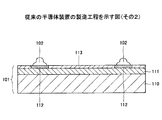
図2〜図10は、従来の半導体装置の製造工程を示す図である。図2〜図10において、図1に示した従来の半導体装置100と同一構成部分には同一符号を付す。
2 to 10 are views showing a manufacturing process of a conventional semiconductor device. 2 to 10, the same components as those of the
始めに、図2に示す工程では、薄板化される前の半導体基板110の表面側に、半導体集積回路111、複数の電極パッド112、及び保護膜113を有した半導体チップ101を形成する。次いで、図3に示す工程では、複数の電極パッド112上に内部接続端子102を形成する。この段階では、複数の内部接続端子102には、高さのばらつきがある。
First, in the step shown in FIG. 2, the
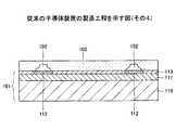
次いで、図4に示す工程では、複数の内部接続端子102に平坦な板115を押し当てて、複数の内部接続端子102の高さを揃える。次いで、図5に示す工程では、内部接続端子102が形成された側の半導体チップ101及び内部接続端子102を覆うように、樹脂層103を形成する。
Next, in the step shown in FIG. 4, the
次いで、図6に示す工程では、内部接続端子102の上面102Aが樹脂層103から露出するまで、樹脂層103を研磨する。このとき、樹脂層103の上面103Aが内部接続端子102の上面102Aと略面一となるように研磨を行う。
Next, in the process illustrated in FIG. 6, the
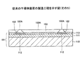
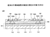
次いで、図7に示す工程では、樹脂層103の上面103Aに配線パターン104を形成する。次いで、図8に示す工程では、外部接続端子配設領域104A以外の部分の配線パターン104を覆うように、樹脂層103上にソルダーレジスト106を形成する。
Next, in the process shown in FIG. 7, the
次いで、図9に示す工程では、半導体基板110の裏面側から半導体基板110を研磨して、半導体基板110を薄板化する。次いで、図10に示す工程では、外部接続端子配設領域104Aに外部接続端子107を形成する。これにより、半導体装置100が製造される(例えば、特許文献1参照。)。
しかしながら、従来の半導体装置100の製造方法では、複数の内部接続端子102の高さを揃える工程や、樹脂層103を研磨して複数の内部接続端子102の上面102Aを樹脂層103から露出させる工程が必要であるため、工程数が増加して、製造コストが増加してしまうという問題があった。
However, in the conventional method for manufacturing the
そこで本発明は、上述した問題点に鑑みなされたものであり、工程数を削減して、製造コストの低減を図ることのできる半導体装置の製造方法を提供することを目的とする。 The present invention has been made in view of the above-described problems, and an object of the present invention is to provide a method for manufacturing a semiconductor device that can reduce the number of steps and reduce the manufacturing cost.
本発明の一観点によれば、複数の半導体チップが形成される半導体基板と、電極パッドを有した前記複数の半導体チップと、前記電極パッドに設けられた内部接続端子と、前記内部接続端子と接続された配線パターンと、を備えた半導体装置の製造方法であって、前記内部接続端子が設けられた側の前記複数の半導体チップと前記内部接続端子とを覆うように絶縁樹脂を形成する絶縁樹脂形成工程と、前記絶縁樹脂上に金属層を形成する金属層形成工程と、前記金属層を押圧して、前記金属層と前記内部接続端子とを圧着させる圧着工程と、前記圧着工程後に、前記金属層をエッチングして前記配線パターンを形成する配線パターン形成工程と、を含むことを特徴とする半導体装置の製造方法が提供される。 According to one aspect of the present invention, a semiconductor substrate on which a plurality of semiconductor chips are formed, the plurality of semiconductor chips having electrode pads, internal connection terminals provided on the electrode pads, and the internal connection terminals A wiring pattern connected to the semiconductor device, wherein the insulating resin is formed so as to cover the plurality of semiconductor chips on the side where the internal connection terminals are provided and the internal connection terminals. A resin forming step, a metal layer forming step of forming a metal layer on the insulating resin, a pressing step of pressing the metal layer and pressing the metal layer and the internal connection terminal, and after the pressing step, And a wiring pattern forming step of forming the wiring pattern by etching the metal layer. A method for manufacturing a semiconductor device is provided.
本発明によれば、内部接続端子が設けられた側の複数の半導体チップと複数の内部接続端子とを覆うように絶縁樹脂を形成後、絶縁樹脂上に配線パターンとなる金属層を形成し、この金属層を押圧して金属層と複数の内部接続端子とを圧着させることにより、複数の内部接続端子の高さを揃える工程、及び複数の内部接続端子の一部を絶縁樹脂から露出させるための絶縁樹脂を研磨する工程が不要となる。これにより、工程数を削減することが可能となるので、半導体装置の製造コストの低減を図ることができる。 According to the present invention, after forming the insulating resin so as to cover the plurality of semiconductor chips on the side provided with the internal connection terminals and the plurality of internal connection terminals, a metal layer to be a wiring pattern is formed on the insulating resin, The step of aligning the height of the plurality of internal connection terminals by pressing the metal layer and crimping the metal layer and the plurality of internal connection terminals, and exposing a part of the plurality of internal connection terminals from the insulating resin The step of polishing the insulating resin becomes unnecessary. As a result, the number of steps can be reduced, and the manufacturing cost of the semiconductor device can be reduced.
本発明の他の観点によれば、複数の半導体チップが形成される半導体基板と、電極パッドを有した前記複数の半導体チップと、前記電極パッドに設けられた内部接続端子と、前記内部接続端子と接続された配線パターンと、を備えた半導体装置の製造方法であって、前記内部接続端子が設けられた側の前記複数の半導体チップと前記内部接続端子とを覆うように絶縁樹脂を形成する絶縁樹脂形成工程と、前記絶縁樹脂上に第1の金属層と第2の金属層とを順次積層させる金属層積層工程と、前記第2の金属層を押圧して、前記第1の金属層と前記内部接続端子とを圧着させる圧着工程と、前記圧着工程後に、前記第2の金属層をエッチングして接続パッドを形成する接続パッド形成工程と、前記第1の金属層をエッチングして前記配線パターンを形成する配線パターン形成工程と、を含むことを特徴とする半導体装置の製造方法が提供される。 According to another aspect of the present invention, a semiconductor substrate on which a plurality of semiconductor chips are formed, the plurality of semiconductor chips having electrode pads, internal connection terminals provided on the electrode pads, and the internal connection terminals A wiring pattern connected to the semiconductor device, wherein an insulating resin is formed so as to cover the plurality of semiconductor chips and the internal connection terminals on the side where the internal connection terminals are provided. An insulating resin forming step; a metal layer laminating step of sequentially laminating a first metal layer and a second metal layer on the insulating resin; and pressing the second metal layer to form the first metal layer A crimping step of crimping the internal connection terminal and the internal connection terminal, a connection pad forming step of etching the second metal layer to form a connection pad after the crimping step, and etching the first metal layer to Wiring putter The method of manufacturing a semiconductor device which comprises a wiring pattern forming step of forming is provided.
本発明によれば、内部接続端子が設けられた側の複数の半導体チップと複数の内部接続端子とを覆うように絶縁樹脂を形成後、絶縁樹脂上に配線パターンとなる第1の金属層と、接続パッドとなる第2の金属層とを順次形成し、第2の金属層を押圧して第1の金属層と複数の内部接続端子とを圧着させることにより、複数の内部接続端子の高さを揃える工程、及び複数の内部接続端子の一部を絶縁樹脂から露出させるための絶縁樹脂を研磨する工程が不要となる。これにより、工程数を削減することが可能となるので、半導体装置の製造コストの低減を図ることができる。 According to the present invention, after forming the insulating resin so as to cover the plurality of semiconductor chips on the side provided with the internal connection terminals and the plurality of internal connection terminals, the first metal layer serving as a wiring pattern on the insulating resin; The second metal layer to be the connection pad is sequentially formed, and the second metal layer is pressed to press the first metal layer and the plurality of internal connection terminals, thereby increasing the height of the plurality of internal connection terminals. The step of aligning the thickness and the step of polishing the insulating resin for exposing a part of the plurality of internal connection terminals from the insulating resin become unnecessary. As a result, the number of steps can be reduced, and the manufacturing cost of the semiconductor device can be reduced.
本発明のその他の観点によれば、複数の半導体チップが形成される半導体基板と、電極パッドを有した前記複数の半導体チップと、前記電極パッドに設けられた内部接続端子と、前記内部接続端子と接続された配線パターンと、を備えた半導体装置の製造方法であって、前記内部接続端子が設けられた側の前記複数の半導体チップと前記内部接続端子とを覆うように絶縁樹脂を形成する絶縁樹脂形成工程と、前記絶縁樹脂上に第1の金属層、第2の金属層、及び前記第2の金属層を保護する保護層を順次積層させる積層工程と、前記積層工程後に、前記保護層を押圧して、前記第1の金属層と前記内部接続端子とを圧着させる圧着工程と、前記圧着工程後に、前記保護層を除去する保護層除去工程と、前記第2の金属層をエッチングして接続パッドを形成する接続パッド形成工程と、前記第1の金属層をエッチングして前記配線パターンを形成する配線パターン形成工程と、を含むことを特徴とする半導体装置の製造方法が提供される。 According to another aspect of the present invention, a semiconductor substrate on which a plurality of semiconductor chips are formed, the plurality of semiconductor chips having electrode pads, internal connection terminals provided on the electrode pads, and the internal connection terminals A wiring pattern connected to the semiconductor device, wherein an insulating resin is formed so as to cover the plurality of semiconductor chips and the internal connection terminals on the side where the internal connection terminals are provided. Insulating resin forming step, laminating step of sequentially laminating a first metal layer, a second metal layer, and a protective layer protecting the second metal layer on the insulating resin, and after the laminating step, the protection Pressing the layer to crimp the first metal layer and the internal connection terminal; after the crimping step, removing the protective layer after removing the protective layer; and etching the second metal layer Connect A connecting pad forming step of forming a head, a method of manufacturing a semiconductor device which comprises a wiring pattern forming step of forming the wiring patterns by etching the first metal layer is provided.
本発明によれば、内部接続端子が設けられた側の複数の半導体チップと複数の内部接続端子とを覆うように絶縁樹脂を形成後、絶縁樹脂上に配線パターンとなる第1の金属層と、接続パッドとなる第2の金属層と、第2の金属層を保護する保護層とを順次形成し、保護層を押圧して第1の金属層と複数の内部接続端子とを圧着させることにより、複数の内部接続端子の高さを揃える工程、及び複数の内部接続端子の一部を絶縁樹脂から露出させるための絶縁樹脂を研磨する工程が不要となる。これにより、工程数を削減することが可能となるので、半導体装置の製造コストの低減を図ることができる。 According to the present invention, after forming the insulating resin so as to cover the plurality of semiconductor chips on the side provided with the internal connection terminals and the plurality of internal connection terminals, the first metal layer serving as a wiring pattern on the insulating resin; Then, a second metal layer to be a connection pad and a protective layer for protecting the second metal layer are sequentially formed, and the first metal layer and the plurality of internal connection terminals are pressure-bonded by pressing the protective layer. This eliminates the steps of aligning the heights of the plurality of internal connection terminals and polishing the insulating resin for exposing a part of the plurality of internal connection terminals from the insulating resin. As a result, the number of steps can be reduced, and the manufacturing cost of the semiconductor device can be reduced.
また、第1の金属層と複数の内部接続端子とを圧着させる際、第2の金属層上に設けられた保護層を押圧することにより、第2の金属層が損傷することを防止できる。 Further, when the first metal layer and the plurality of internal connection terminals are pressure-bonded, it is possible to prevent the second metal layer from being damaged by pressing the protective layer provided on the second metal layer.
本発明のその他の観点によれば、複数の半導体チップが形成される半導体基板と、電極パッドを有した前記複数の半導体チップと、前記電極パッドに設けられた内部接続端子と、前記内部接続端子と接続された配線パターンと、を備えた半導体装置の製造方法であって、前記内部接続端子が設けられた側の前記複数の半導体チップと前記内部接続端子とを覆うように絶縁樹脂を形成する絶縁樹脂形成工程と、前記絶縁樹脂上に第1の金属層、第2の金属層、及び第3の金属層を順次積層させる金属層積層工程と、前記第3の金属層を押圧して、前記第1の金属層と前記内部接続端子とを圧着させる圧着工程と、前記圧着工程後に、第3の金属層をエッチングしてメタルポストを形成するメタルポスト形成工程と、前記第2の金属層をエッチングして接続パッドを形成する接続パッド形成工程と、前記第1の金属層をエッチングして前記配線パターンを形成する配線パターン形成工程と、を含むことを特徴とする半導体装置の製造方法が提供される。 According to another aspect of the present invention, a semiconductor substrate on which a plurality of semiconductor chips are formed, the plurality of semiconductor chips having electrode pads, internal connection terminals provided on the electrode pads, and the internal connection terminals A wiring pattern connected to the semiconductor device, wherein an insulating resin is formed so as to cover the plurality of semiconductor chips and the internal connection terminals on the side where the internal connection terminals are provided. An insulating resin forming step, a metal layer laminating step of sequentially laminating a first metal layer, a second metal layer, and a third metal layer on the insulating resin, pressing the third metal layer, A crimping step for crimping the first metal layer and the internal connection terminal; a metal post forming step for etching the third metal layer to form a metal post after the crimping step; and the second metal layer. Ethen There is provided a method for manufacturing a semiconductor device, comprising: a connection pad forming step for forming a connection pad; and a wiring pattern forming step for etching the first metal layer to form the wiring pattern. The
本発明によれば、内部接続端子が設けられた側の複数の半導体チップと複数の内部接続端子とを覆うように絶縁樹脂を形成後、絶縁樹脂上に配線パターンとなる第1の金属層と、接続パッドとなる第2の金属層と、メタルポストとなる第3の金属層とを順次形成し、第3の金属層を押圧して第1の金属層と複数の内部接続端子とを圧着させることにより、複数の内部接続端子の高さを揃える工程、及び複数の内部接続端子の一部を絶縁樹脂から露出させるための絶縁樹脂を研磨する工程が不要となる。これにより、工程数を削減することが可能となるので、半導体装置の製造コストの低減を図ることができる。 According to the present invention, after forming the insulating resin so as to cover the plurality of semiconductor chips on the side provided with the internal connection terminals and the plurality of internal connection terminals, the first metal layer serving as a wiring pattern on the insulating resin; Then, a second metal layer to be a connection pad and a third metal layer to be a metal post are sequentially formed, and the first metal layer and the plurality of internal connection terminals are crimped by pressing the third metal layer. By doing so, the steps of aligning the heights of the plurality of internal connection terminals and the step of polishing the insulating resin for exposing a part of the plurality of internal connection terminals from the insulating resin become unnecessary. As a result, the number of steps can be reduced, and the manufacturing cost of the semiconductor device can be reduced.
また、接続パッド上にメタルポストを形成することにより、例えば、メタルポスト上にマザーボード等の実装基板と接続される外部接続端子を設けた場合、外部接続端子にかかるストレス(応力)を緩和することができる。 In addition, by forming a metal post on the connection pad, for example, when an external connection terminal connected to a mounting board such as a mother board is provided on the metal post, the stress applied to the external connection terminal is relieved. Can do.
本発明のその他の観点によれば、複数の半導体チップが形成される半導体基板と、電極パッドを有した前記複数の半導体チップと、前記電極パッドに設けられた内部接続端子と、前記内部接続端子と接続された配線パターンと、を備えた半導体装置の製造方法であって、前記内部接続端子が設けられた側の前記複数の半導体チップと前記内部接続端子とを覆うように異方性導電樹脂を形成する異方性導電樹脂形成工程と、前記異方性導電樹脂上に金属層を形成する金属層形成工程と、前記金属層を押圧して、前記金属層と前記内部接続端子とを圧着させる圧着工程と、前記圧着工程後に、前記金属層をエッチングして前記配線パターンを形成する配線パターン形成工程と、を含むことを特徴とする半導体装置の製造方法が提供される。 According to another aspect of the present invention, a semiconductor substrate on which a plurality of semiconductor chips are formed, the plurality of semiconductor chips having electrode pads, internal connection terminals provided on the electrode pads, and the internal connection terminals A wiring pattern connected to the semiconductor device, wherein the anisotropic conductive resin covers the plurality of semiconductor chips and the internal connection terminals on the side where the internal connection terminals are provided. Forming an anisotropic conductive resin, forming a metal layer on the anisotropic conductive resin, pressing the metal layer, and crimping the metal layer and the internal connection terminal There is provided a method for manufacturing a semiconductor device, comprising: a crimping step of forming a wiring pattern; and a wiring pattern forming step of etching the metal layer to form the wiring pattern after the crimping step.
本発明によれば、内部接続端子が設けられた側の複数の半導体チップと複数の内部接続端子とを覆うように異方性導電樹脂を形成後、異方性導電樹脂上に配線パターンとなる金属層を形成し、この金属層を押圧して金属層と複数の内部接続端子とを圧着させることにより、複数の内部接続端子の高さを揃える工程、及び複数の内部接続端子の一部を異方性導電樹脂から露出させるための絶縁樹脂を研磨する工程が不要となる。これにより、工程数を削減することが可能となるので、半導体装置の製造コストの低減を図ることができる。 According to the present invention, after forming the anisotropic conductive resin so as to cover the plurality of semiconductor chips on the side where the internal connection terminals are provided and the plurality of internal connection terminals, a wiring pattern is formed on the anisotropic conductive resin. Forming a metal layer, pressing the metal layer and crimping the metal layer and the plurality of internal connection terminals, aligning the height of the plurality of internal connection terminals, and a part of the plurality of internal connection terminals A step of polishing the insulating resin for exposing from the anisotropic conductive resin becomes unnecessary. As a result, the number of steps can be reduced, and the manufacturing cost of the semiconductor device can be reduced.
また、異方性導電樹脂を用いることにより、絶縁樹脂を用いた場合と比較して、金属層を押圧するときの圧力を小さくすることが可能となるので、半導体装置を容易に製造することができる。 In addition, the use of anisotropic conductive resin makes it possible to reduce the pressure when pressing the metal layer as compared with the case where insulating resin is used, so that the semiconductor device can be easily manufactured. it can.
本発明のその他の観点によれば、複数の半導体チップが形成される半導体基板と、電極パッドを有した前記複数の半導体チップと、前記電極パッドに設けられた内部接続端子と、前記内部接続端子と接続された配線パターンと、を備えた半導体装置の製造方法であって、前記内部接続端子が設けられた側の前記複数の半導体チップと前記内部接続端子とを覆うように異方性導電樹脂を形成する異方性導電樹脂形成工程と、前記異方性導電樹脂に第1の金属層と第2の金属層とを順次積層させる金属層積層工程と、前記第2の金属層を押圧して、前記第1の金属層と前記内部接続端子とを圧着させる圧着工程と、前記圧着工程後に、前記第2の金属層をエッチングして接続パッドを形成する接続パッド形成工程と、前記第1の金属層をエッチングして前記配線パターンを形成する配線パターン形成工程と、を含むことを特徴とする半導体装置の製造方法が提供される。 According to another aspect of the present invention, a semiconductor substrate on which a plurality of semiconductor chips are formed, the plurality of semiconductor chips having electrode pads, internal connection terminals provided on the electrode pads, and the internal connection terminals A wiring pattern connected to the semiconductor device, wherein the anisotropic conductive resin covers the plurality of semiconductor chips and the internal connection terminals on the side where the internal connection terminals are provided. Forming an anisotropic conductive resin, a metal layer laminating step of sequentially laminating a first metal layer and a second metal layer on the anisotropic conductive resin, and pressing the second metal layer A crimping step for crimping the first metal layer and the internal connection terminal, a connection pad forming step for etching the second metal layer to form a connection pad after the crimping step, and the first Etched metal layer The method of manufacturing a semiconductor device which comprises a wiring pattern forming step of forming the wiring pattern is provided with.
本発明によれば、内部接続端子が設けられた側の複数の半導体チップと複数の内部接続端子とを覆うように異方性導電樹脂を形成後、異方性導電樹脂上に配線パターンとなる第1の金属層と、接続パッドとなる第2の金属層とを順次形成し、第2の金属層を押圧して第1の金属層と複数の内部接続端子とを圧着させることにより、複数の内部接続端子の高さを揃える工程、及び複数の内部接続端子の一部を異方性導電樹脂から露出させるための異方性導電樹脂を研磨する工程が不要となる。これにより、工程数を削減することが可能となるので、半導体装置の製造コストの低減を図ることができる。 According to the present invention, after forming the anisotropic conductive resin so as to cover the plurality of semiconductor chips on the side where the internal connection terminals are provided and the plurality of internal connection terminals, a wiring pattern is formed on the anisotropic conductive resin. By sequentially forming a first metal layer and a second metal layer to be a connection pad and pressing the second metal layer to crimp the first metal layer and the plurality of internal connection terminals, a plurality of The steps of aligning the heights of the internal connection terminals and the step of polishing the anisotropic conductive resin for exposing a part of the plurality of internal connection terminals from the anisotropic conductive resin are not required. As a result, the number of steps can be reduced, and the manufacturing cost of the semiconductor device can be reduced.
本発明のその他の観点によれば、複数の半導体チップが形成される半導体基板と、電極パッドを有した前記複数の半導体チップと、前記電極パッドに設けられた内部接続端子と、前記内部接続端子と接続された配線パターンと、を備えた半導体装置の製造方法であって、前記内部接続端子が設けられた側の前記複数の半導体チップと前記内部接続端子とを覆うように異方性導電樹脂を形成する異方性導電樹脂形成工程と、前記異方性導電樹脂に第1の金属層、第2の金属層、及び前記第2の金属層を保護する保護層を順次積層させる積層工程と、前記積層工程後に、前記保護層を押圧して、前記第1の金属層と前記内部接続端子とを圧着させる圧着工程と、前記圧着工程後に、前記保護層を除去する保護層除去工程と、前記第2の金属層をエッチングして接続パッドを形成する接続パッド形成工程と、前記第1の金属層をエッチングして前記配線パターンを形成する配線パターン形成工程と、を含むことを特徴とする半導体装置の製造方法が提供される。 According to another aspect of the present invention, a semiconductor substrate on which a plurality of semiconductor chips are formed, the plurality of semiconductor chips having electrode pads, internal connection terminals provided on the electrode pads, and the internal connection terminals A wiring pattern connected to the semiconductor device, wherein the anisotropic conductive resin covers the plurality of semiconductor chips and the internal connection terminals on the side where the internal connection terminals are provided. Forming an anisotropic conductive resin, and laminating a first metal layer, a second metal layer, and a protective layer for protecting the second metal layer on the anisotropic conductive resin in sequence. A pressure-bonding step of pressing the protective layer after the lamination step to pressure-bond the first metal layer and the internal connection terminal; a protective layer removing step of removing the protective layer after the pressure-bonding step; The second metal layer is etched. A method of manufacturing a semiconductor device, comprising: a connection pad forming step of forming a connection pad by etching; and a wiring pattern forming step of etching the first metal layer to form the wiring pattern. Is done.
本発明によれば、内部接続端子が設けられた側の複数の半導体チップと複数の内部接続端子とを覆うように異方性導電樹脂を形成後、異方性導電樹脂上に配線パターンとなる第1の金属層と、接続パッドとなる第2の金属層と、第2の金属層を保護する保護層とを順次形成し、保護層を押圧して第1の金属層と複数の内部接続端子とを圧着させることにより、複数の内部接続端子の高さを揃える工程、及び複数の内部接続端子の一部を異方性導電樹脂から露出させるための異方性導電樹脂を研磨する工程が不要となる。これにより、工程数を削減することが可能となるので、半導体装置の製造コストの低減を図ることができる。 According to the present invention, after forming the anisotropic conductive resin so as to cover the plurality of semiconductor chips on the side where the internal connection terminals are provided and the plurality of internal connection terminals, a wiring pattern is formed on the anisotropic conductive resin. A first metal layer, a second metal layer serving as a connection pad, and a protective layer for protecting the second metal layer are sequentially formed, and the first metal layer and a plurality of internal connections are pressed by pressing the protective layer The steps of aligning the heights of the plurality of internal connection terminals by crimping the terminals and polishing the anisotropic conductive resin for exposing a part of the plurality of internal connection terminals from the anisotropic conductive resin It becomes unnecessary. As a result, the number of steps can be reduced, and the manufacturing cost of the semiconductor device can be reduced.
また、第1の金属層と複数の内部接続端子とを圧着させる際、第2の金属層上に設けられた保護層を押圧することにより、第2の金属層が損傷することを防止できる。 Further, when the first metal layer and the plurality of internal connection terminals are pressure-bonded, it is possible to prevent the second metal layer from being damaged by pressing the protective layer provided on the second metal layer.
本発明のその他の観点によれば、複数の半導体チップが形成される半導体基板と、電極パッドを有した前記複数の半導体チップと、前記電極パッドに設けられた内部接続端子と、前記内部接続端子と接続された配線パターンと、を備えた半導体装置の製造方法であって、前記内部接続端子が設けられた側の前記複数の半導体チップと前記内部接続端子とを覆うように異方性導電樹脂を形成する異方性導電樹脂形成工程と、前記異方性導電樹脂に第1の金属層、第2の金属層、及び第3の金属層を順次積層させる金属層積層工程と、前記第3の金属層を押圧して、前記第1の金属層と前記内部接続端子とを圧着させる圧着工程と、前記圧着工程後に、前記第3の金属層をエッチングしてメタルポストを形成するメタルポスト形成工程と、前記第2の金属層をエッチングして接続パッドを形成する接続パッド形成工程と、前記第1の金属層をエッチングして前記配線パターンを形成する配線パターン形成工程と、を含むことを特徴とする半導体装置の製造方法が提供される。 According to another aspect of the present invention, a semiconductor substrate on which a plurality of semiconductor chips are formed, the plurality of semiconductor chips having electrode pads, internal connection terminals provided on the electrode pads, and the internal connection terminals A wiring pattern connected to the semiconductor device, wherein the anisotropic conductive resin covers the plurality of semiconductor chips and the internal connection terminals on the side where the internal connection terminals are provided. Forming an anisotropic conductive resin, a metal layer stacking step of sequentially stacking a first metal layer, a second metal layer, and a third metal layer on the anisotropic conductive resin, and the third Pressing the metal layer to crimp the first metal layer and the internal connection terminal, and forming the metal post by etching the third metal layer after the crimping step. And the step A connection pad forming step of forming a connection pad by etching the metal layer; and a wiring pattern forming step of forming the wiring pattern by etching the first metal layer. A manufacturing method is provided.
本発明によれば、内部接続端子が設けられた側の複数の半導体チップと複数の内部接続端子とを覆うように異方性導電樹脂を形成後、異方性導電樹脂上に配線パターンとなる第1の金属層と、接続パッドとなる第2の金属層と、メタルポストとなる第3の金属層とを順次形成し、第3の金属層を押圧して第1の金属層と複数の内部接続端子とを圧着させることにより、複数の内部接続端子の高さを揃える工程、及び複数の内部接続端子の一部を異方性導電樹脂から露出させるための異方性導電樹脂を研磨する工程が不要となる。これにより、工程数を削減することが可能となるので、半導体装置の製造コストの低減を図ることができる。 According to the present invention, after forming the anisotropic conductive resin so as to cover the plurality of semiconductor chips on the side where the internal connection terminals are provided and the plurality of internal connection terminals, a wiring pattern is formed on the anisotropic conductive resin. A first metal layer, a second metal layer serving as a connection pad, and a third metal layer serving as a metal post are sequentially formed, and the third metal layer is pressed to form the first metal layer and a plurality of metal layers. The step of aligning the heights of the plurality of internal connection terminals by crimping the internal connection terminals, and polishing the anisotropic conductive resin for exposing a part of the plurality of internal connection terminals from the anisotropic conductive resin A process becomes unnecessary. As a result, the number of steps can be reduced, and the manufacturing cost of the semiconductor device can be reduced.
また、接続パッド上にメタルポストを形成することにより、例えば、メタルポスト上にマザーボード等の実装基板と接続される外部接続端子を設けた場合、外部接続端子にかかるストレス(応力)を緩和することができる。 In addition, by forming a metal post on the connection pad, for example, when an external connection terminal connected to a mounting board such as a mother board is provided on the metal post, the stress applied to the external connection terminal is relieved. Can do.
本発明によれば、工程数を削減して、半導体装置の製造コストの低減を図ることができる。 According to the present invention, it is possible to reduce the number of steps and reduce the manufacturing cost of a semiconductor device.
次に、図面に基づいて本発明の実施の形態について説明する。 Next, embodiments of the present invention will be described with reference to the drawings.
(第1の実施の形態)
図11は、本発明の第1の実施の形態に係る半導体装置の断面図である。
(First embodiment)
FIG. 11 is a cross-sectional view of the semiconductor device according to the first embodiment of the present invention.
図11を参照するに、第1の実施の形態の半導体装置10は、半導体チップ11と、内部接続端子12と、絶縁樹脂13と、配線パターン14,15と、ソルダーレジスト16と、外部接続端子17とを有する。
Referring to FIG. 11, the
半導体チップ11は、半導体基板21と、半導体集積回路22と、電極パッド23と、保護膜24とを有する。半導体基板21は、半導体集積回路22を形成するための基板である。半導体基板21は、薄板化されている。半導体基板21の厚さT1は、例えば、100μm〜300μmとすることができる。半導体基板21は、例えば、薄板化されたSiウエハが個片化されたものである。
The
半導体集積回路22は、半導体基板21の表面側に設けられている。半導体集積回路22は、半導体基板21に形成された拡散層(図示せず)、半導体基板21上に積層された絶縁層(図示せず)、及び積層された絶縁層に設けられたビア(図示せず)及び配線等(図示せず)から構成されている。
The semiconductor integrated
電極パッド23は、半導体集積回路22上に複数設けられている。電極パッド23は、半導体集積回路22に設けられた配線(図示せず)と電気的に接続されている。電極パッド23の材料としては、例えば、Alを用いることができる。
A plurality of
保護膜24は、半導体集積回路22上に設けられている。保護膜24は、半導体集積回路22を保護するための膜である。保護膜24としては、例えば、SiN膜やPSG膜等を用いることができる。
The
内部接続端子12は、電極パッド23上に設けられている。内部接続端子12は、半導体集積回路22と配線パターン14とを電気的に接続するためのものである。内部接続端子12の高さH1は、例えば、10μm〜60μmとすることができる。内部接続端子12としては、例えば、Auバンプ、Auめっき膜、無電解めっき法により形成されたNi膜とそれを覆うAu膜から構成される金属膜等を用いることができる。Auバンプは、例えば、ボンディング法やめっき法により形成することができる。
The
絶縁樹脂13は、内部接続端子12の上面12Aを除く内部接続端子12部分及び半導体チップ11上を覆うように設けられている。内部接続端子12の上面12Aは、絶縁樹脂13から露出されている。絶縁樹脂13の上面13Aは、内部接続端子12の上面12Aと略面一とされている。絶縁樹脂13としては、例えば、粘着性を有したシート状の絶縁樹脂(例えば、NCF(Non Conductive Film))や、ペースト状の絶縁樹脂(例えば、NCP(Non Conductive Paste))等を用いることができる。絶縁樹脂13の厚さT2は、例えば、10μm〜60μmとすることができる。
The insulating
配線パターン14は、内部接続端子12の上面12Aと接触するように、絶縁樹脂13の上面13Aに設けられている。配線パターン14は、内部接続端子12を介して、半導体集積回路22と電気的に接続されている。配線パターン14は、外部接続端子17が配設される外部接続端子配設領域14Aを有する。
The
配線パターン15は、絶縁樹脂13の上面13Aに設けられている。配線パターン15は、外部接続端子17が配設される外部接続端子配設領域15Aを有する。配線パターン14,15の材料としては、例えば、Cuを用いることができる。配線パターン14,15の厚さは、例えば、12μmとすることができる。
The
ソルダーレジスト16は、外部接続端子配設領域14A,15Aを除く配線パターン14,15部分を覆うように絶縁樹脂13上に設けられている。ソルダーレジスト16は、外部接続端子配設領域14Aを露出する開口部16Aと、外部接続端子配設領域15Aを露出する開口部16Bとを有する。
The solder resist 16 is provided on the insulating
外部接続端子17は、配線パターン14,15の外部接続端子配設領域14A,15Aに設けられている。外部接続端子17は、マザーボード等の実装基板(図示せず)に設けられたパッドと電気的に接続される端子である。外部接続端子17としては、例えば、はんだバンプを用いることができる。
The
図12〜図22は、本発明の第1の実施の形態に係る半導体装置の製造工程を示す図であり、図23は、半導体基板の平面図である。図12〜図23において、第1の実施の形態の半導体装置10と同一構成部分には同一符号を付す。また、図12〜図23において、Cはダイサーが半導体基板31を切断する位置(以下、「切断位置C」とする)を示している。
12 to 22 are views showing a manufacturing process of the semiconductor device according to the first embodiment of the present invention, and FIG. 23 is a plan view of the semiconductor substrate. 12 to 23, the same components as those of the
始めに、図12に示す工程では、複数の半導体装置形成領域Aと、複数の半導体装置形成領域Aを分離するスクライブ領域Bとを有した半導体基板31を準備する(図23参照)。半導体装置形成領域Aは、半導体装置10が形成される領域である。半導体基板31は、薄板化され、かつ切断位置Cにおいて切断されることにより、先に説明した半導体基板21(図11参照)となるものである。半導体基板31としては、例えば、Siウエハを用いることができる。半導体基板31の厚さT3は、例えば、500μm〜775μmとすることができる。
First, in the step shown in FIG. 12, a
次いで、図13に示す工程では、半導体装置形成領域Aに対応する半導体基板31の表面側に、周知の手法により、半導体集積回路22、電極パッド23、及び保護膜24を有した半導体チップ11を形成する。電極パッド23の材料としては、例えば、Alを用いることができる。また、保護膜24としては、例えば、SiN膜やPSG膜等を用いることができる。
Next, in the process shown in FIG. 13, the
次いで、図14に示す工程では、複数の半導体装置形成領域Aに設けられた複数の電極パッド23上にそれぞれ内部接続端子12を形成する。内部接続端子12としては、例えば、Auバンプ、Auめっき膜、無電解めっき法により形成されたNi膜とそれを覆うAu膜から構成される金属膜等を用いることができる。
Auバンプは、例えば、ボンディング法により形成することができる。なお、図14に示す工程で形成された複数の内部接続端子12には、高さばらつきが存在する。
Next, in the process shown in FIG. 14, the
The Au bump can be formed by, for example, a bonding method. Note that there are height variations in the plurality of
次いで、図15に示す工程では、内部接続端子12が設けられた側の複数の半導体チップ11(複数の半導体チップ11の表面側)及び内部接続端子12を覆うように絶縁樹脂13を形成する(絶縁樹脂形成工程)。絶縁樹脂13としては、粘着性を有したシート状の絶縁樹脂(例えば、NCF(Non Conductive Film))や、ペースト状の絶縁樹脂(例えば、NCP(Non Conductive Paste))等を用いることができる。粘着性を有したシート状の絶縁樹脂を用いた場合は、図14に示す構造体の上面側にシート状の絶縁樹脂を貼り付けることで絶縁樹脂13を形成する。また、絶縁樹脂13としてペースト状の絶縁樹脂を用いた場合は、図15に示す構造体の上面側に印刷法によりペースト状の絶縁樹脂を形成し、その後、プリベークして絶縁樹脂を半硬化させる。この半硬化した絶縁樹脂は、接着性を有する。絶縁樹脂13の厚さT4は、例えば、20μm〜100μmとすることができる。
Next, in the step shown in FIG. 15, the insulating
次いで、図16に示す工程では、絶縁樹脂13の上面13Aに金属層33を形成する(金属層形成工程)。金属層33は、後述する図18に示す工程において、エッチングされて配線パターン14,15となるものである。具体的には、金属層33としてCu箔を用意し、このCu箔を絶縁樹脂13の上面13Aに貼り付ける。金属層33の厚さT5は、例えば、10μmとすることができる。
Next, in a step shown in FIG. 16, a
次いで、図17に示す工程では、図17に示す構造体を加熱した状態で、金属層33の上面33A側から金属層33を押圧して、金属層33の下面33Bと複数の内部接続端子12の上面12Aとを接触させて、金属層33と内部接続端子12とを圧着させる(圧着工程)。また、図17に示す構造体を加熱することにより、絶縁樹脂13は硬化する。圧着後の絶縁樹脂13の厚さT2は、例えば、10μm〜60μmとすることができる。
Next, in the process shown in FIG. 17, the
このように、絶縁樹脂13上に配線パターン14,15となる金属層33を形成し、金属層33を押圧して金属層33と複数の内部接続端子12とを圧着させることにより、従来行われていた複数の内部接続端子12の高さを揃える工程、及び複数の内部接続端子12の上端部を絶縁樹脂13から露出させるための絶縁樹脂を研磨する工程が不要となる。これにより、半導体装置10の製造工程数を削減することが可能となるので、半導体装置10の製造コストの低減を図ることができる。
As described above, the
次いで、図18に示す工程では、金属層33をエッチングによりパターニングして、複数の半導体装置形成領域Aに配線パターン14,15を形成(配線パターン形成工程)し、その後、配線パターン14,15の粗化処理を行う。
Next, in the process shown in FIG. 18, the
具体的には、金属層33上にパターニングされたレジスト膜を形成し、次いで、このレジスト膜をマスクとして、金属層33をエッチングして配線パターン14,15を形成する。配線パターン14,15の粗化処理は、黒化処理又は粗化エッチング処理のいずれかの方法により行うことができる。上記粗化処理は、配線パターン14,15の上面及び側面に形成されるソルダーレジスト16と配線パターン14,15との密着性を向上させるためのものである。
Specifically, a patterned resist film is formed on the
次いで、図19に示す工程では、外部接続端子配設領域14A,15Aを除いた配線パターン14,15部分と絶縁樹脂13上とを覆うように、ソルダーレジスト16を形成する。
Next, in the step shown in FIG. 19, the solder resist 16 is formed so as to cover the
次いで、図20に示す工程では、半導体基板31の裏面側から半導体基板31を研磨又は研削して、半導体基板31を薄板化する。半導体基板31の薄板化には、例えば、バックサイドグラインダーを用いることができる。薄板化後の半導体基板31の厚さT6は、例えば、100μm〜300μmとすることができる。
Next, in the process illustrated in FIG. 20, the
次いで、図21に示す工程では、配線パターン14,15の外部接続端子配設領域14A,15Aに外部接続端子17を形成する。これにより、複数の半導体装置形成領域Aに半導体装置10に相当する構造体が形成される。
Next, in the process shown in FIG. 21, the
次いで、図22に示す工程では、半導体基板31を切断位置Cに沿って切断する。これにより、複数の半導体装置10が製造される。
Next, in the step shown in FIG. 22, the
本実施の形態の半導体装置の製造方法によれば、内部接続端子12が設けられた側の複数の半導体チップ11(複数の半導体チップ11の表面側)及び内部接続端子12を覆うように絶縁樹脂13を形成後、絶縁樹脂13上に配線パターン14,15となる金属層33を形成し、金属層33を押圧して金属層33と複数の内部接続端子12とを圧着させることにより、複数の内部接続端子12の高さを揃える工程、及び複数の内部接続端子12の上端部を絶縁樹脂13から露出させるための絶縁樹脂を研磨する工程を行う必要がなくなるため、工程数を削減して、半導体装置10の製造コストの低減を図ることができる。
According to the manufacturing method of the semiconductor device of the present embodiment, the insulating resin covers the plurality of
(第2の実施の形態)
図24は、本発明の第2の実施の形態に係る半導体装置の断面図である。
(Second Embodiment)
FIG. 24 is a cross-sectional view of a semiconductor device according to the second embodiment of the present invention.
図24を参照するに、第2の実施の形態の半導体装置40は、第1の実施の形態の半導体装置10に設けられた絶縁樹脂13の代わりに、異方性導電樹脂41を設けた以外は半導体装置10と同様に構成される。
Referring to FIG. 24, the
異方性導電樹脂41としては、例えば、粘着性を有したシート状の異方性導電樹脂(例えば、ACF(Anisotropic Conductive Film))や、ペースト状の異方性導電樹脂(例えば、ACP(Anisotropic Conductive Paste))等を用いることができる。ACP及びACFは、エポキシ系樹脂をベースとする絶縁樹脂にNi/Auに被膜された小径球状の樹脂が分散されたものであり、鉛直方向に対しては導電性を有し、水平方向には絶縁性を有する樹脂である。異方性導電樹脂41の厚さT7は、例えば、10μm〜60μmとすることができる。
Examples of the anisotropic
図25〜図27は、本発明の第2の実施の形態に係る半導体装置の製造工程を示す図である。図25〜図27において、第2の実施の形態の半導体装置40と同一構成部分には同一符号を付す。
25 to 27 are views showing a manufacturing process of the semiconductor device according to the second embodiment of the present invention. 25 to 27, the same components as those of the
図25〜図27を参照して、第2の実施の形態の半導体装置40の製造方法について説明する。始めに、第1の実施の形態で説明した図12〜図14に示す工程と同様な処理を行って、図14に示す構造体を形成する。
A method for manufacturing the
次いで、図25に示す工程では、内部接続端子12が設けられた側の複数の半導体チップ11(複数の半導体チップ11の表面側)及び内部接続端子12を覆うように異方性導電樹脂41を形成する(異方性導電樹脂形成工程)。異方性導電樹脂41としては、例えば、粘着性を有したシート状の異方性導電樹脂(例えば、ACF(Anisotropic Conductive Film))や、ペースト状の異方性導電樹脂(例えば、ACP(Anisotropic Conductive Paste))等を用いることができる。
Next, in the process shown in FIG. 25, the anisotropic
異方性導電樹脂41としてペースト状の異方性導電樹脂(例えば、ACP(Anisotropic Conductive Paste))を用いた場合は、例えば、印刷法によりペースト状の異方性導電樹脂を形成後、ペースト状の異方性導電樹脂をプリベークして半硬化させる。半硬化した異方性導電樹脂は、接着剤としての機能を有する。異方性導電樹脂41の厚さT8は、例えば、20μm〜100μmとすることができる。
When a paste-like anisotropic conductive resin (for example, ACP (Anisotropic Conductive Paste)) is used as the anisotropic
次いで、図26に示す工程では、異方性導電樹脂41の上面41Aに金属層33を形成する(金属層形成工程)。具体的には、金属層33としてCu箔を用意し、異方性導電樹脂41の上面41AにCu箔を貼り付ける。金属層33の厚さT5は、例えば、10μmとすることができる。
Next, in the step shown in FIG. 26, the
次いで、図27に示す工程では、図26に示す構造体を加熱した状態で、金属層33の上面33A側から金属層33を押圧し、金属層33の下面33Bと複数の内部接続端子12の上面12Aとを接触させて、金属層33と複数の内部接続端子12とを圧着させる(圧着工程)。また、図26に示す構造体を加熱することにより、異方性導電樹脂41は硬化する。圧着後の異方性導電樹脂41の厚さT7は、例えば、10μm〜60μmとすることができる。
Next, in the step shown in FIG. 27, the
このように、内部接続端子12が設けられた側の複数の半導体チップ11(複数の半導体チップ11の表面側)及び内部接続端子12を覆うように異方性導電樹脂41を形成後、異方性導電樹脂41上に配線パターン14,15となる金属層33を形成し、金属層33を押圧して金属層33と複数の内部接続端子12とを圧着させることにより、絶縁樹脂を用いた場合と比較して、金属層33を押圧するときの圧力を小さくすることが可能となるため、半導体装置40を容易に製造することができる。
As described above, the anisotropic
その後、第1の実施の形態で説明した図18〜図22に示す工程と同様な処理を行うことにより、複数の半導体装置40が製造される。
Thereafter, a plurality of
本実施の形態の半導体装置の製造方法によれば、内部接続端子12が設けられた側の複数の半導体チップ11(複数の半導体チップ11の表面側)及び内部接続端子12を覆うように異方性導電樹脂41を形成後、異方性導電樹脂41上に配線パターン14,15となる金属層33を形成し、金属層33を押圧して金属層33と複数の内部接続端子12とを圧着させることにより、複数の内部接続端子12の高さを揃える工程、及び複数の内部接続端子12の上端部を異方性導電樹脂41から露出させるための異方性導電樹脂を研磨する工程を行う必要がなくなるため、工程数を削減して、半導体装置40の製造コストの低減を図ることができる。
According to the method for manufacturing a semiconductor device of the present embodiment, the
また、第1の実施の形態の半導体装置10に設けられた絶縁樹脂13の代わりに異方性導電樹脂41を設けることにより、金属層33を押圧するときの圧力を小さくすることが可能となるため、半導体装置40を容易に製造することができる。
Further, by providing the anisotropic
(第3の実施の形態)
図28は、本発明の第3の実施の形態に係る半導体装置の断面図である。
(Third embodiment)
FIG. 28 is a sectional view of a semiconductor device according to the third embodiment of the present invention.
図28を参照するに、第3の実施の形態の半導体装置50は、第1の実施の形態の半導体装置10の構成に、さらに接続パッド51を設けた以外は半導体装置10と同様に構成される。
Referring to FIG. 28, the
接続パッド51は、配線パターン14,15の外部接続端子配設領域14A,15Aに設けられている。接続パッド51は、ソルダーレジスト16に形成された開口部16A,16Bから露出されている。接続パッド51上には、外部接続端子17が配設されている。接続パッド51の材料としては、例えば、Sn、Ni、Ti等を用いることができる。接続パッド51の厚さは、例えば、2μmとすることができる。
The
図29〜図34は、本発明の第3の実施の形態に係る半導体装置の製造工程を示す図である。図29〜図34において、第3の実施の形態の半導体装置50と同一構成部分には同一符号を付す。
FIGS. 29 to 34 are views showing manufacturing steps of the semiconductor device according to the third embodiment of the invention. 29 to 34, the same components as those of the
図29〜図34を参照して、第3の実施の形態の半導体装置50の製造方法について説明する。始めに、第1の実施の形態で説明した図12〜図15に示す工程と同様な処理を行って、図15に示す構造体を形成する。
A method for manufacturing the
次いで、図29に示す工程では、絶縁樹脂13の上面13Aに第1の金属層54と第2の金属層55とを順次形成する(金属層積層工程)。第1の金属層54は、エッチングによりパターニングされて配線パターン14,15となる金属層である。また、第1の金属層54は、第2の金属層55をエッチングするときのエッチングストッパーとなる。第2の金属層55は、エッチングによりパターニングされて接続パッド51となる金属層である。
Next, in the step shown in FIG. 29, the
第2の金属層55として、例えば、Sn層、Ni層、Ti層等を用いた場合、第1の金属層54としては、例えば、Cu層を用いることができる。具体的には、例えば、Cu箔(第1の金属層54に相当する)上にSn層(第2の金属55に相当する)が形成されたシート状の金属箔を絶縁樹脂13の上面13Aに貼り付けることで、第1及び第2の金属層54,55を形成する。第1の金属層54の厚さT9は、例えば、10μmとすることができる。また、第2の金属層55の厚さT10は、例えば、2μmとすることができる。
For example, when an Sn layer, a Ni layer, a Ti layer, or the like is used as the
次いで、図30に示す工程では、図29に示す構造体を加熱した状態で、第2の金属層55を押圧して、第1の金属層54の下面54Aと複数の内部接続端子12の上面12Aとを接触させて、第1の金属層54と複数の内部接続端子12とを圧着させる(圧着工程)。また、図29に示す構造体を加熱することにより、絶縁樹脂13は硬化する。圧着後の絶縁樹脂13の厚さT2は、例えば、10μm〜60μmとすることができる。
Next, in the process shown in FIG. 30, the
このように、第2の金属層55を押圧して、配線パターン14,15となる第1の金属層54と複数の内部接続端子12とを圧着させることにより、従来、必要であった複数の内部接続端子12の高さを揃える工程、及び複数の内部接続端子12の上端部を絶縁樹脂13から露出させるための絶縁樹脂13を研磨する工程が不要となるため、製造工程数を削減することが可能となるので、半導体装置50の製造コストの低減を図ることができる。
In this way, by pressing the
次いで、図31に示す工程では、第2の金属層55をエッチングによりパターニングして、外部接続端子配設領域14A,15Aに対応する部分の第1の金属層54上に接続パッド51を形成する(接続パッド形成工程)。具体的には、第2の金属層55上にパターニングされたレジスト膜を形成し、このレジスト膜をマスクとする異方性エッチングにより、第2の金属層55をエッチングして接続パッド51を形成する。
Next, in the step shown in FIG. 31, the
このとき、第1の金属層54が第2の金属層55をエッチングする際のエッチングストッパーとして機能するため、絶縁樹脂13がエッチングされることを防止することができる。
At this time, since the
次いで、図32に示す工程では、図31に示す構造体上にパターニングされたレジスト膜57を形成する。レジスト膜57は、第1の金属膜54をエッチングして配線パターン14,15を形成する際のマスクである。
Next, in a step shown in FIG. 32, a patterned resist
次いで、図33に示す工程では、レジスト膜57をマスクとして、第1の金属層54をエッチングして、配線パターン14,15を形成する(配線パターン形成工程)。
Next, in the step shown in FIG. 33, the
次いで、図34に示す工程では、レジスト膜57を除去する。その後、第1の実施の形態で説明した図20〜図22に示す工程と同様な処理を行うことにより、複数の半導体装置50が製造される。
Next, in a step shown in FIG. 34, the resist
本実施の形態の半導体装置の製造方法によれば、複数の内部接続端子12が設けられた側の複数の半導体チップ11と複数の内部接続端子12とを覆うように絶縁樹脂13を形成後、絶縁樹脂13上に配線パターン14,15となる第1の金属層54と、接続パッド51となる第2の金属層55とを順次形成し、第2の金属層55を押圧して、第1の金属層54と複数の内部接続端子12とを圧着させることにより、複数の内部接続端子12の高さを揃える工程、及び複数の内部接続端子12の一部を絶縁樹脂13から露出させるための絶縁樹脂13を研磨する工程が不要となるため、工程数を削減することが可能となり、半導体装置50の製造コストの低減を図ることができる。
According to the manufacturing method of the semiconductor device of the present embodiment, after forming the insulating
なお、本実施の形態の半導体装置50では、配線パターン14,15と半導体チップ11の間に絶縁樹脂13を設けた場合を例に挙げて説明したが、絶縁樹脂13の代わりに第2の実施の形態で説明した異方性導電樹脂41を設けてもよい。この場合、第2の実施の形態の半導体装置40の製造方法と同様な効果を得ることができる。
In the
図35〜図37は、本発明の第3の実施の形態に係る半導体装置の製造工程の変形例を示す図である。図35〜図37において、先に説明した図29に示す構造体と同一構成部分には同一符号を付す。 35 to 37 are views showing modifications of the manufacturing process of the semiconductor device according to the third embodiment of the present invention. 35 to 37, the same components as those of the structure shown in FIG. 29 described above are denoted by the same reference numerals.
図35〜図37を参照して、本発明の第3の実施の形態に係る半導体装置50の製造方法の変形例について説明する。始めに、第1の実施の形態で説明した図12〜図15に示す工程と同様な処理を行って、図15に示す構造体を形成する。
With reference to FIGS. 35-37, the modification of the manufacturing method of the
次いで、図35に示す工程では、絶縁樹脂13の上面13Aに、第1の金属層54、第2の金属層55、及び保護層61を順次形成する(積層工程)。保護層61は、第2の金属層55を保護するためのものである。保護層61は、第2の金属層55に対して接着力の弱い接着剤で貼り付けられている。これにより、保護層61は、第2の金属層55から容易に剥がすことが可能な構成とされている。保護層61としては、例えば、Cu箔を用いることができる。また、保護層61の厚さT11は、例えば、35μm〜100μmとすることができる。
Next, in the step shown in FIG. 35, the
次いで、図36に示す工程では、図35に示す構造体を加熱した状態で、保護層61を押圧して、第1の金属層54の下面54Aと複数の内部接続端子12の上面12Aとを接触させて、第1の金属層54と複数の内部接続端子12とを圧着させる(圧着工程)。また、図35に示す構造体を加熱することにより、絶縁樹脂13は硬化する。圧着後の絶縁樹脂13の厚さT2は、例えば、10μm〜60μmとすることができる。
Next, in the step shown in FIG. 36, the
このように、第2の金属層55上に設けた保護層61を押圧して、配線パターン14,15となる第1の金属層54と複数の内部接続端子12とを圧着させることにより、圧着工程において、厚さの薄い第2の金属層55が損傷することを防止できる。
In this way, the
次いで、図37に示す工程では、保護層61を除去する(保護層除去工程)。その後、先に説明した図31〜図34に示す工程と同様な処理を行い、続いて、第1の実施の形態で説明した図20〜図22に示す工程と同様な処理を行うことにより、複数の半導体装置50が製造される。
Next, in the step shown in FIG. 37, the
本実施の形態の半導体装置の製造工程の変形例によれば、第2の金属層55上に保護層61を形成し、この保護層61を押圧して、配線パターン14,15となる第1の金属層54と複数の内部接続端子12とを圧着させることにより、厚さの薄い第2の金属層55が損傷することを防止できる。
According to the modification of the manufacturing process of the semiconductor device of the present embodiment, the
(第4の実施の形態)
図38は、本発明の第4の実施の形態に係る半導体装置の断面図である。
(Fourth embodiment)
FIG. 38 is a sectional view of a semiconductor device according to the fourth embodiment of the present invention.
図38を参照するに、第4の実施の形態の半導体装置70は、第3の実施の形態の半導体装置50に設けられたソルダーレジスト16の代わりに封止樹脂72を設けると共に、さらにメタルポスト71を設けた以外は半導体装置50と同様に構成される。
Referring to FIG. 38, in the
メタルポスト71は、接続パッド51上に設けられている。メタルポスト71の側面は、封止樹脂72により覆われている。メタルポスト71の上面71Aは、封止樹脂72から露出されている。メタルポスト71の上面71Aは、封止樹脂72の上面72Aと略面一とされている。メタルポスト71の上面71Aには、外部接続端子17が設けられている。
The
メタルポスト71は、外部接続端子17と接続パッド51とを電気的に接続している。メタルポスト71は、外部接続端子17がマザーボード等の実装基板(図示せず)と接続された際に外部接続端子17が受けるストレス(応力)を緩和する機能を有する。メタルポスト71の材料としては、例えば、Cuを用いることができる。メタルポスト71の高さH2は、50μm〜100μmとすることができる。
The
封止樹脂72は、配線パターン14,15、接続パッド51、及びメタルポスト71の側面を覆うように、絶縁樹脂13上に設けられている。封止樹脂72としては、例えば、トランスファーモールド法やコンプレッションモールド法により形成されたエポキシ樹脂を用いることができる。
The sealing
図39〜図49は、本発明の第4の実施の形態に係る半導体装置の製造工程を示す図である。図39〜図49において、第3の実施の形態で説明した図35に示す構造体と同一構成部分には同一符号を付す。 39 to 49 are views showing manufacturing steps of the semiconductor device according to the fourth embodiment of the present invention. 39 to 49, the same components as those of the structure shown in FIG. 35 described in the third embodiment are denoted by the same reference numerals.
図39〜図49を参照して、第4の実施の形態の半導体装置70の製造方法について説明する。始めに、第1の実施の形態で説明した図12〜図15に示す工程と同様な処理を行って、図15に示す構造体を形成する。
With reference to FIGS. 39 to 49, a method for manufacturing the
次いで、図39に示す工程では、絶縁樹脂13の上面13Aに第1の金属層54、第2の金属層55、及び第3の金属層74を順次形成する(金属層積層工程)。第1の金属層54は、第2の金属層55をエッチングして接続パッド51を形成する際、エッチングストッパーとして機能する。第1の金属層54の材料としては、例えば、Cuを用いることができる。また、第1の金属層54の厚さT9は、例えば、10μmとすることができる。
Next, in the step shown in FIG. 39, the
第2の金属層55は、第3の金属層74をエッチングしてメタルポスト71を形成する際、エッチングストッパーとなる金属層である。第2の金属層55の材料としては、例えば、Sn、Ni、Ti等を用いることができる。また、第2の金属層55の厚さT10は、例えば、2μmとすることができる。
The
第3の金属層74は、エッチングによりパターニングされてメタルポスト71となる金属層である。第3の金属層74の材料としては、例えば、Cuを用いることができる。第3の金属層74の厚さT12は、例えば、50μm〜100μmとすることができる。
The
例えば、Cu箔(第1の金属層54に相当する)上に、Sn層(第2の金属55に相当する)、他のCu箔(第3の金属層74に相当する)が積層されたシート状の金属箔を絶縁樹脂13の上面13Aに貼り付けることで、第1〜第3の金属層54,55,74を形成する。
For example, an Sn layer (corresponding to the second metal 55) and another Cu foil (corresponding to the third metal layer 74) are laminated on the Cu foil (corresponding to the first metal layer 54). By sticking a sheet-like metal foil to the
次いで、図40に示す工程では、図39に示す構造体を加熱した状態で、第3の金属層74を押圧して、第1の金属層54の下面54Aと複数の内部接続端子12の上面12Aとを接触させて、第1の金属層54と複数の内部接続端子12とを圧着させる(圧着工程)。また、図39に示す構造体を加熱することにより、絶縁樹脂13は硬化する。圧着後の絶縁樹脂13の厚さT2は、例えば、10μm〜60μmとすることができる。
Next, in the step shown in FIG. 40, the
このように、複数の内部接続端子12が設けられた側の複数の半導体チップ11と複数の内部接続端子12とを覆うように絶縁樹脂13を形成後、絶縁樹脂13上に配線パターン14,15となる第1の金属層54と、第2の金属層55と、第3の金属層74とを順次形成し、第3の金属層74を押圧して、第1の金属層54と複数の内部接続端子12とを圧着させることにより、複数の内部接続端子12の高さを揃える工程、及び複数の内部接続端子12の一部を絶縁樹脂13から露出させるための絶縁樹脂13を研磨する工程が不要となるため、工程数を削減することが可能となり、半導体装置70の製造コストの低減を図ることができる。
Thus, after forming the insulating
次いで、図41に示す工程では、メタルポスト71の形成領域に対応する第3の金属層74上に、パターニングされたレジスト膜76を形成する。次いで、図42に示す工程では、レジスト膜76をマスクとして、第3の金属層74をエッチングすることにより、レジスト膜76の下方にメタルポスト71を形成する(メタルポスト形成工程)。
Next, in a step shown in FIG. 41, a patterned resist
このとき、第2の金属層55が第3の金属層74をエッチングする際のエッチングストッパーとして機能するため、第3の金属層74のエッチング時に第2の金属層55がエッチングされることを防止できる。
At this time, since the
次いで、図43に示す工程では、レジスト膜76をマスクとして、第2の金属層55をエッチングすることにより、接続パッド51を形成する(接続パッド形成工程)。
Next, in the step shown in FIG. 43, the
このとき、第1の金属層54が第2の金属層55をエッチングする際のエッチングストッパーとして機能するため、第2の金属層55のエッチング時に第1の金属層54がエッチングされることを防止できる。
At this time, since the
次いで、図44に示す工程では、レジスト膜76を除去する。次いで、図45に示す工程では、図44に示す構造体上に、パターニングされたレジスト膜78を形成する。レジスト膜78は、第1の金属層54をエッチングして配線パターン14,15を形成する際のマスクである。
Next, in a step shown in FIG. 44, the resist
次いで、図46に示す工程では、レジスト膜78をマスクとして、第1の金属層54をエッチングして配線パターン14,15を形成する(配線パターン形成工程)。次いで、図47に示す工程では、レジスト膜78を除去する。
46, the
次いで、図48に示す工程では、図47に示した構造体の上面側を覆うように封止樹脂72を形成する。封止樹脂72は、例えば、トランスファーモールド法やコンプレッションモールド法により形成することができる。封止樹脂72としては、例えば、エポキシ樹脂を用いることができる。
48, a sealing
次いで、図49に示す工程では、メタルポスト71の上面71Aと封止樹脂72の上面72Aとが略面一となるように、不要な封止樹脂72を除去する。具体的には、例えば、プラズマアッシングにより、不要な封止樹脂72を除去する。
49, unnecessary sealing
その後、第1の実施の形態で説明した図20〜図22に示す工程と同様な処理を行うことにより、複数の半導体装置70が製造される。
Thereafter, a plurality of
本実施の形態の半導体装置の製造方法によれば、複数の内部接続端子12が設けられた側の複数の半導体チップ11と複数の内部接続端子12とを覆うように絶縁樹脂13を形成後、絶縁樹脂13上に配線パターン14,15となる第1の金属層54と、第2の金属層55と、第3の金属層74とを順次形成し、第3の金属層74を押圧して、第1の金属層54と複数の内部接続端子12とを圧着させることにより、複数の内部接続端子12の高さを揃える工程、及び複数の内部接続端子12の一部を絶縁樹脂13から露出させるための絶縁樹脂13を研磨する工程が不要となるため、工程数を削減することが可能となり、半導体装置70の製造コストの低減を図ることができる。
According to the manufacturing method of the semiconductor device of the present embodiment, after forming the insulating
また、外部接続端子17と接続パッド51との間にメタルポスト71を形成することにより、外部接続端子17が受けるストレス(応力)を緩和することができる。
Further, by forming the
なお、本実施の形態の半導体装置70では、配線パターン14,15と半導体チップ11の間に絶縁樹脂13を設けた場合を例に挙げて説明したが、絶縁樹脂13の代わりに第2の実施の形態で説明した異方性導電樹脂41を設けてもよい。この場合、第2の実施の形態の半導体装置40の製造方法と同様な効果を得ることができる。
In the
以上、本発明の好ましい実施の形態について詳述したが、本発明はかかる特定の実施の形態に限定されるものではなく、特許請求の範囲内に記載された本発明の要旨の範囲内において、種々の変形・変更が可能である。 The preferred embodiments of the present invention have been described in detail above, but the present invention is not limited to such specific embodiments, and within the scope of the present invention described in the claims, Various modifications and changes are possible.
本発明は、平面視した状態で半導体チップと略同じ大きさであり、半導体チップが配線パターンにフリップチップ接続された半導体装置の製造方法に適用できる。 The present invention can be applied to a method of manufacturing a semiconductor device that is substantially the same size as a semiconductor chip in a plan view and is flip-chip connected to a wiring pattern.
10,40,50,70 半導体装置
11 半導体チップ
12 内部接続端子
12A,13A,33A,41A,71A,72A 上面
13 絶縁樹脂
14,15 配線パターン
14A,15A 外部接続端子配設領域
16 ソルダーレジスト
16A,16B 開口部
17 外部接続端子
21,31 半導体基板
22 半導体集積回路
23 電極パッド
24 保護膜
33 金属層
33B,54A 下面
41 異方性導電樹脂
51 接続パッド
54 第1の金属層
55 第2の金属層
57,76,78 レジスト膜
61 保護層
71 メタルポスト
72 封止樹脂
74 第3の金属層
A 半導体装置形成領域
B スクライブ領域
C 切断位置
T1〜T12 厚さ
H1,H2 高さ
10, 40, 50, 70
Claims (14)
前記内部接続端子が設けられた側の前記複数の半導体チップと前記内部接続端子とを覆うように絶縁樹脂を形成する絶縁樹脂形成工程と、
前記絶縁樹脂上に第1の金属層と第2の金属層とを順次積層させる金属層積層工程と、
前記第2の金属層を押圧して、前記第1の金属層と前記内部接続端子とを圧着させる圧着工程と、
前記圧着工程後に、前記第2の金属層をエッチングして接続パッドを形成する接続パッド形成工程と、
前記第1の金属層をエッチングして前記配線パターンを形成する配線パターン形成工程と、を含むことを特徴とする半導体装置の製造方法。 A semiconductor substrate on which a plurality of semiconductor chips are formed, the plurality of semiconductor chips having electrode pads, an internal connection terminal provided on the electrode pad, and a wiring pattern connected to the internal connection terminal. A method for manufacturing a semiconductor device comprising:
An insulating resin forming step of forming an insulating resin so as to cover the plurality of semiconductor chips on the side where the internal connection terminals are provided and the internal connection terminals;
A metal layer laminating step of sequentially laminating a first metal layer and a second metal layer on the insulating resin;
A crimping step of pressing the second metal layer and crimping the first metal layer and the internal connection terminal;
A connection pad forming step of forming a connection pad by etching the second metal layer after the crimping step;
And a wiring pattern forming step of forming the wiring pattern by etching the first metal layer.
前記内部接続端子が設けられた側の前記複数の半導体チップと前記内部接続端子とを覆うように絶縁樹脂を形成する絶縁樹脂形成工程と、
前記絶縁樹脂上に第1の金属層、第2の金属層、及び前記第2の金属層を保護する保護層を順次積層させる積層工程と、
前記積層工程後に、前記保護層を押圧して、前記第1の金属層と前記内部接続端子とを圧着させる圧着工程と、
前記圧着工程後に、前記保護層を除去する保護層除去工程と、
前記第2の金属層をエッチングして接続パッドを形成する接続パッド形成工程と、
前記第1の金属層をエッチングして前記配線パターンを形成する配線パターン形成工程と、を含むことを特徴とする半導体装置の製造方法。 A semiconductor substrate on which a plurality of semiconductor chips are formed, the plurality of semiconductor chips having electrode pads, an internal connection terminal provided on the electrode pad, and a wiring pattern connected to the internal connection terminal. A method for manufacturing a semiconductor device comprising:
An insulating resin forming step of forming an insulating resin so as to cover the plurality of semiconductor chips on the side where the internal connection terminals are provided and the internal connection terminals;
A laminating step of sequentially laminating a first metal layer, a second metal layer, and a protective layer protecting the second metal layer on the insulating resin;
After the laminating step, pressing the protective layer to crimp the first metal layer and the internal connection terminal; and
A protective layer removing step for removing the protective layer after the crimping step;
A connection pad forming step of etching the second metal layer to form a connection pad;
And a wiring pattern forming step of forming the wiring pattern by etching the first metal layer.
前記内部接続端子が設けられた側の前記複数の半導体チップと前記内部接続端子とを覆うように絶縁樹脂を形成する絶縁樹脂形成工程と、
前記絶縁樹脂上に第1の金属層、第2の金属層、及び第3の金属層を順次積層させる金属層積層工程と、
前記第3の金属層を押圧して、前記第1の金属層と前記内部接続端子とを圧着させる圧着工程と、
前記圧着工程後に、第3の金属層をエッチングしてメタルポストを形成するメタルポスト形成工程と、
前記第2の金属層をエッチングして接続パッドを形成する接続パッド形成工程と、
前記第1の金属層をエッチングして前記配線パターンを形成する配線パターン形成工程と、を含むことを特徴とする半導体装置の製造方法。 A semiconductor substrate on which a plurality of semiconductor chips are formed, the plurality of semiconductor chips having electrode pads, an internal connection terminal provided on the electrode pad, and a wiring pattern connected to the internal connection terminal. A method for manufacturing a semiconductor device comprising:
An insulating resin forming step of forming an insulating resin so as to cover the plurality of semiconductor chips on the side where the internal connection terminals are provided and the internal connection terminals;
A metal layer laminating step of sequentially laminating a first metal layer, a second metal layer, and a third metal layer on the insulating resin;
A crimping step of pressing the third metal layer to crimp the first metal layer and the internal connection terminal;
A metal post forming step of forming a metal post by etching the third metal layer after the crimping step;
A connection pad forming step of etching the second metal layer to form a connection pad;
And a wiring pattern forming step of forming the wiring pattern by etching the first metal layer.
前記内部接続端子が設けられた側の前記複数の半導体チップと前記内部接続端子とを覆うように異方性導電樹脂を形成する異方性導電樹脂形成工程と、
前記異方性導電樹脂に第1の金属層と第2の金属層とを順次積層させる金属層積層工程と、
前記第2の金属層を押圧して、前記第1の金属層と前記内部接続端子とを圧着させる圧着工程と、
前記圧着工程後に、前記第2の金属層をエッチングして接続パッドを形成する接続パッド形成工程と、
前記第1の金属層をエッチングして前記配線パターンを形成する配線パターン形成工程と、を含むことを特徴とする半導体装置の製造方法。 A semiconductor substrate on which a plurality of semiconductor chips are formed, the plurality of semiconductor chips having electrode pads, an internal connection terminal provided on the electrode pad, and a wiring pattern connected to the internal connection terminal. A method for manufacturing a semiconductor device comprising:
Forming an anisotropic conductive resin so as to cover the plurality of semiconductor chips on the side where the internal connection terminals are provided and the internal connection terminals; and
A metal layer laminating step of sequentially laminating a first metal layer and a second metal layer on the anisotropic conductive resin;
A crimping step of pressing the second metal layer and crimping the first metal layer and the internal connection terminal;
A connection pad forming step of forming a connection pad by etching the second metal layer after the crimping step;
And a wiring pattern forming step of forming the wiring pattern by etching the first metal layer.
前記内部接続端子が設けられた側の前記複数の半導体チップと前記内部接続端子とを覆うように異方性導電樹脂を形成する異方性導電樹脂形成工程と、
前記異方性導電樹脂に第1の金属層、第2の金属層、及び前記第2の金属層を保護する保護層を順次積層させる積層工程と、
前記積層工程後に、前記保護層を押圧して、前記第1の金属層と前記内部接続端子とを圧着させる圧着工程と、
前記圧着工程後に、前記保護層を除去する保護層除去工程と、
前記第2の金属層をエッチングして接続パッドを形成する接続パッド形成工程と、
前記第1の金属層をエッチングして前記配線パターンを形成する配線パターン形成工程と、を含むことを特徴とする半導体装置の製造方法。 A semiconductor substrate on which a plurality of semiconductor chips are formed, the plurality of semiconductor chips having electrode pads, an internal connection terminal provided on the electrode pad, and a wiring pattern connected to the internal connection terminal. A method for manufacturing a semiconductor device comprising:
Forming an anisotropic conductive resin so as to cover the plurality of semiconductor chips on the side where the internal connection terminals are provided and the internal connection terminals; and
A laminating step of sequentially laminating a first metal layer, a second metal layer, and a protective layer protecting the second metal layer on the anisotropic conductive resin;
After the laminating step, pressing the protective layer to crimp the first metal layer and the internal connection terminal; and
A protective layer removing step for removing the protective layer after the crimping step;
A connection pad forming step of etching the second metal layer to form a connection pad;
And a wiring pattern forming step of forming the wiring pattern by etching the first metal layer.
前記内部接続端子が設けられた側の前記複数の半導体チップと前記内部接続端子とを覆うように異方性導電樹脂を形成する異方性導電樹脂形成工程と、
前記異方性導電樹脂に第1の金属層、第2の金属層、及び第3の金属層を順次積層させる金属層積層工程と、
前記第3の金属層を押圧して、前記第1の金属層と前記内部接続端子とを圧着させる圧着工程と、
前記圧着工程後に、前記第3の金属層をエッチングしてメタルポストを形成するメタルポスト形成工程と、
前記第2の金属層をエッチングして接続パッドを形成する接続パッド形成工程と、
前記第1の金属層をエッチングして前記配線パターンを形成する配線パターン形成工程と、を含むことを特徴とする半導体装置の製造方法。 A semiconductor substrate on which a plurality of semiconductor chips are formed, the plurality of semiconductor chips having electrode pads, an internal connection terminal provided on the electrode pad, and a wiring pattern connected to the internal connection terminal. A method for manufacturing a semiconductor device comprising:
Forming an anisotropic conductive resin so as to cover the plurality of semiconductor chips on the side where the internal connection terminals are provided and the internal connection terminals; and
A metal layer laminating step of sequentially laminating a first metal layer, a second metal layer, and a third metal layer on the anisotropic conductive resin;
A crimping step of pressing the third metal layer to crimp the first metal layer and the internal connection terminal;
A metal post forming step of forming a metal post by etching the third metal layer after the crimping step;
A connection pad forming step of etching the second metal layer to form a connection pad;
And a wiring pattern forming step of forming the wiring pattern by etching the first metal layer.
Priority Applications (6)
| Application Number | Priority Date | Filing Date | Title |
|---|---|---|---|
| JP2006260948A JP4105202B2 (en) | 2006-09-26 | 2006-09-26 | Manufacturing method of semiconductor device |
| KR1020070093990A KR20080028283A (en) | 2006-09-26 | 2007-09-17 | Manufacturing method of semiconductor device |
| US11/856,360 US7749889B2 (en) | 2006-09-26 | 2007-09-17 | Manufacturing method of semiconductor device |
| EP07018290A EP1906445A3 (en) | 2006-09-26 | 2007-09-18 | Manufacturing method of semiconductor device |
| TW096135324A TW200818358A (en) | 2006-09-26 | 2007-09-21 | Manufacturing method of semiconductor device |
| CN2007101541921A CN101154606B (en) | 2006-09-26 | 2007-09-24 | Manufacturing method of semiconductor device |
Applications Claiming Priority (1)
| Application Number | Priority Date | Filing Date | Title |
|---|---|---|---|
| JP2006260948A JP4105202B2 (en) | 2006-09-26 | 2006-09-26 | Manufacturing method of semiconductor device |
Publications (2)
| Publication Number | Publication Date |
|---|---|
| JP2008084958A JP2008084958A (en) | 2008-04-10 |
| JP4105202B2 true JP4105202B2 (en) | 2008-06-25 |
Family
ID=38847000
Family Applications (1)
| Application Number | Title | Priority Date | Filing Date |
|---|---|---|---|
| JP2006260948A Expired - Fee Related JP4105202B2 (en) | 2006-09-26 | 2006-09-26 | Manufacturing method of semiconductor device |
Country Status (6)
| Country | Link |
|---|---|
| US (1) | US7749889B2 (en) |
| EP (1) | EP1906445A3 (en) |
| JP (1) | JP4105202B2 (en) |
| KR (1) | KR20080028283A (en) |
| CN (1) | CN101154606B (en) |
| TW (1) | TW200818358A (en) |
Families Citing this family (11)
| Publication number | Priority date | Publication date | Assignee | Title |
|---|---|---|---|---|
| CN101303443A (en) * | 2007-05-11 | 2008-11-12 | 鸿富锦精密工业(深圳)有限公司 | Camera module group and assembling method thereof |
| JP4121542B1 (en) * | 2007-06-18 | 2008-07-23 | 新光電気工業株式会社 | Manufacturing method of electronic device |
| JP5064157B2 (en) * | 2007-09-18 | 2012-10-31 | 新光電気工業株式会社 | Manufacturing method of semiconductor device |
| JP2010010249A (en) | 2008-06-25 | 2010-01-14 | Shinko Electric Ind Co Ltd | Semiconductor device, and method of manufacturing the same |
| WO2010073800A1 (en) | 2008-12-22 | 2010-07-01 | 富士通株式会社 | Electronic component and method for manufacturing same |
| JP2012134270A (en) * | 2010-12-21 | 2012-07-12 | Shinko Electric Ind Co Ltd | Semiconductor device and manufacturing method of the same |
| JP2015076446A (en) * | 2013-10-07 | 2015-04-20 | 日立化成株式会社 | Solar battery cell |
| US10163828B2 (en) * | 2013-11-18 | 2018-12-25 | Taiwan Semiconductor Manufacturing Company Ltd. | Semiconductor device and fabricating method thereof |
| KR102256299B1 (en) | 2016-08-02 | 2021-05-26 | 삼성에스디아이 주식회사 | Lithium cobalt composite oxide for lithium secondary battery and lithium secondary battery including positive electrode comprising the same |
| KR102256296B1 (en) * | 2016-08-02 | 2021-05-26 | 삼성에스디아이 주식회사 | Lithium cobalt composite oxide for lithium secondary battery and lithium secondary battery including positive electrode comprising the same |
| JP6784330B2 (en) * | 2017-06-20 | 2020-11-11 | 株式会社村田製作所 | Module and its manufacturing method |
Family Cites Families (13)
| Publication number | Priority date | Publication date | Assignee | Title |
|---|---|---|---|---|
| US4503112A (en) * | 1981-06-12 | 1985-03-05 | Oak Industries Inc. | Printed circuit material |
| US5517752A (en) * | 1992-05-13 | 1996-05-21 | Fujitsu Limited | Method of connecting a pressure-connector terminal of a device with a terminal electrode of a substrate |
| KR100218996B1 (en) | 1995-03-24 | 1999-09-01 | 모기 쥰이찌 | Semiconductor device |
| JP3378171B2 (en) | 1997-06-02 | 2003-02-17 | 山一電機株式会社 | Semiconductor package manufacturing method |
| JP3780688B2 (en) | 1998-02-27 | 2006-05-31 | 日立化成工業株式会社 | CSP substrate manufacturing method |
| KR100711539B1 (en) * | 1999-06-10 | 2007-04-27 | 도요 고한 가부시키가이샤 | Clad plate for forming interposer for semiconductor device, interposer for semiconductor device, and method of manufacturing them |
| JP2001308095A (en) | 2000-04-19 | 2001-11-02 | Toyo Kohan Co Ltd | Semiconductor device and method of manufacture |
| JP2002110854A (en) | 2000-09-28 | 2002-04-12 | Nec Corp | Semiconductor device and its manufacturing method |
| JP2002151551A (en) * | 2000-11-10 | 2002-05-24 | Hitachi Ltd | Flip-chip mounting structure, semiconductor device therewith and mounting method |
| JP3717899B2 (en) * | 2002-04-01 | 2005-11-16 | Necエレクトロニクス株式会社 | Semiconductor device and manufacturing method thereof |
| JP3614828B2 (en) | 2002-04-05 | 2005-01-26 | 沖電気工業株式会社 | Manufacturing method of chip size package |
| JP2004193297A (en) | 2002-12-11 | 2004-07-08 | Dainippon Printing Co Ltd | Wafer level package and its manufacturing method |
| JP2004193497A (en) * | 2002-12-13 | 2004-07-08 | Nec Electronics Corp | Chip-size package and manufacturing method thereof |
-
2006
- 2006-09-26 JP JP2006260948A patent/JP4105202B2/en not_active Expired - Fee Related
-
2007
- 2007-09-17 KR KR1020070093990A patent/KR20080028283A/en not_active Application Discontinuation
- 2007-09-17 US US11/856,360 patent/US7749889B2/en not_active Expired - Fee Related
- 2007-09-18 EP EP07018290A patent/EP1906445A3/en not_active Withdrawn
- 2007-09-21 TW TW096135324A patent/TW200818358A/en unknown
- 2007-09-24 CN CN2007101541921A patent/CN101154606B/en not_active Expired - Fee Related
Also Published As
| Publication number | Publication date |
|---|---|
| EP1906445A2 (en) | 2008-04-02 |
| CN101154606A (en) | 2008-04-02 |
| US7749889B2 (en) | 2010-07-06 |
| CN101154606B (en) | 2011-04-13 |
| EP1906445A3 (en) | 2009-11-25 |
| JP2008084958A (en) | 2008-04-10 |
| US20080076207A1 (en) | 2008-03-27 |
| TW200818358A (en) | 2008-04-16 |
| KR20080028283A (en) | 2008-03-31 |
Similar Documents
| Publication | Publication Date | Title |
|---|---|---|
| JP4105202B2 (en) | Manufacturing method of semiconductor device | |
| JP5064157B2 (en) | Manufacturing method of semiconductor device | |
| KR100621438B1 (en) | Stack chip package using photo sensitive polymer and manufacturing method thereof | |
| US8410614B2 (en) | Semiconductor device having a semiconductor element buried in an insulating layer and method of manufacturing the same | |
| TWI652780B (en) | Package structure and manufacturing method thereof | |
| US7790515B2 (en) | Semiconductor device with no base member and method of manufacturing the same | |
| US8211754B2 (en) | Semiconductor device and manufacturing method thereof | |
| JP5135246B2 (en) | Semiconductor module, method for manufacturing the same, and portable device | |
| KR20080069712A (en) | Circuit device and method for manufacturing circuit device | |
| JP5423020B2 (en) | SEMICONDUCTOR DEVICE, SEMICONDUCTOR DEVICE MANUFACTURING METHOD, AND ELECTRONIC DEVICE | |
| JP4828515B2 (en) | Manufacturing method of semiconductor device | |
| JP5064158B2 (en) | Semiconductor device and manufacturing method thereof | |
| JP4753960B2 (en) | Semiconductor module and method for manufacturing semiconductor module | |
| JP2013165087A (en) | Semiconductor module and semiconductor module manufacturing method | |
| JP5139039B2 (en) | Semiconductor device and manufacturing method thereof | |
| JP5048420B2 (en) | Semiconductor device and manufacturing method thereof | |
| JP2008147367A (en) | Semiconductor device and its manufacturing method | |
| JP2004063808A (en) | Package structure of semiconductor device and its manufacturing method | |
| US20100248429A1 (en) | Method for manufacturing semiconductor modules |
Legal Events
| Date | Code | Title | Description |
|---|---|---|---|
| A521 | Request for written amendment filed |
Free format text: JAPANESE INTERMEDIATE CODE: A523 Effective date: 20080123 |
|
| A871 | Explanation of circumstances concerning accelerated examination |
Free format text: JAPANESE INTERMEDIATE CODE: A871 Effective date: 20080123 |
|
| TRDD | Decision of grant or rejection written | ||
| A975 | Report on accelerated examination |
Free format text: JAPANESE INTERMEDIATE CODE: A971005 Effective date: 20080311 |
|
| A01 | Written decision to grant a patent or to grant a registration (utility model) |
Free format text: JAPANESE INTERMEDIATE CODE: A01 Effective date: 20080318 |
|
| A61 | First payment of annual fees (during grant procedure) |
Free format text: JAPANESE INTERMEDIATE CODE: A61 Effective date: 20080326 |
|
| R150 | Certificate of patent or registration of utility model |
Ref document number: 4105202 Country of ref document: JP Free format text: JAPANESE INTERMEDIATE CODE: R150 Free format text: JAPANESE INTERMEDIATE CODE: R150 |
|
| FPAY | Renewal fee payment (event date is renewal date of database) |
Free format text: PAYMENT UNTIL: 20110404 Year of fee payment: 3 |
|
| FPAY | Renewal fee payment (event date is renewal date of database) |
Free format text: PAYMENT UNTIL: 20120404 Year of fee payment: 4 |
|
| FPAY | Renewal fee payment (event date is renewal date of database) |
Free format text: PAYMENT UNTIL: 20130404 Year of fee payment: 5 |
|
| FPAY | Renewal fee payment (event date is renewal date of database) |
Free format text: PAYMENT UNTIL: 20130404 Year of fee payment: 5 |
|
| FPAY | Renewal fee payment (event date is renewal date of database) |
Free format text: PAYMENT UNTIL: 20140404 Year of fee payment: 6 |
|
| LAPS | Cancellation because of no payment of annual fees |