JP5048420B2 - Semiconductor device and manufacturing method thereof - Google Patents
Semiconductor device and manufacturing method thereof Download PDFInfo
- Publication number
- JP5048420B2 JP5048420B2 JP2007212949A JP2007212949A JP5048420B2 JP 5048420 B2 JP5048420 B2 JP 5048420B2 JP 2007212949 A JP2007212949 A JP 2007212949A JP 2007212949 A JP2007212949 A JP 2007212949A JP 5048420 B2 JP5048420 B2 JP 5048420B2
- Authority
- JP
- Japan
- Prior art keywords
- internal connection
- connection terminal
- wiring pattern
- metal layer
- recess
- Prior art date
- Legal status (The legal status is an assumption and is not a legal conclusion. Google has not performed a legal analysis and makes no representation as to the accuracy of the status listed.)
- Active
Links
- 239000004065 semiconductor Substances 0.000 title claims description 224
- 238000004519 manufacturing process Methods 0.000 title claims description 61
- 239000002184 metal Substances 0.000 claims description 150
- 238000003825 pressing Methods 0.000 claims description 47
- 239000000758 substrate Substances 0.000 claims description 38
- 238000000034 method Methods 0.000 claims description 36
- 230000002093 peripheral effect Effects 0.000 claims description 24
- 229910000679 solder Inorganic materials 0.000 claims description 18
- 238000005530 etching Methods 0.000 claims description 12
- 239000011347 resin Substances 0.000 description 28
- 229920005989 resin Polymers 0.000 description 28
- 230000001681 protective effect Effects 0.000 description 11
- 230000015572 biosynthetic process Effects 0.000 description 8
- 238000005498 polishing Methods 0.000 description 8
- 238000009792 diffusion process Methods 0.000 description 6
- 238000007747 plating Methods 0.000 description 5
- XUIMIQQOPSSXEZ-UHFFFAOYSA-N Silicon Chemical compound [Si] XUIMIQQOPSSXEZ-UHFFFAOYSA-N 0.000 description 4
- 229910045601 alloy Inorganic materials 0.000 description 4
- 239000000956 alloy Substances 0.000 description 4
- 238000005520 cutting process Methods 0.000 description 4
- 238000010586 diagram Methods 0.000 description 4
- 238000009413 insulation Methods 0.000 description 4
- 229910052710 silicon Inorganic materials 0.000 description 4
- 239000010703 silicon Substances 0.000 description 4
- 239000000853 adhesive Substances 0.000 description 3
- 230000001070 adhesive effect Effects 0.000 description 3
- 238000007772 electroless plating Methods 0.000 description 3
- RYGMFSIKBFXOCR-UHFFFAOYSA-N Copper Chemical compound [Cu] RYGMFSIKBFXOCR-UHFFFAOYSA-N 0.000 description 2
- 229910018594 Si-Cu Inorganic materials 0.000 description 2
- 229910008465 Si—Cu Inorganic materials 0.000 description 2
- 230000007423 decrease Effects 0.000 description 2
- 230000000694 effects Effects 0.000 description 2
- 239000000463 material Substances 0.000 description 2
- 230000002265 prevention Effects 0.000 description 2
- 238000007796 conventional method Methods 0.000 description 1
- 238000001312 dry etching Methods 0.000 description 1
- 238000012986 modification Methods 0.000 description 1
- 230000004048 modification Effects 0.000 description 1
- 238000002360 preparation method Methods 0.000 description 1
- 238000001039 wet etching Methods 0.000 description 1
Images


Classifications
-
- H—ELECTRICITY
- H01—ELECTRIC ELEMENTS
- H01L—SEMICONDUCTOR DEVICES NOT COVERED BY CLASS H10
- H01L23/00—Details of semiconductor or other solid state devices
- H01L23/28—Encapsulations, e.g. encapsulating layers, coatings, e.g. for protection
- H01L23/31—Encapsulations, e.g. encapsulating layers, coatings, e.g. for protection characterised by the arrangement or shape
- H01L23/3107—Encapsulations, e.g. encapsulating layers, coatings, e.g. for protection characterised by the arrangement or shape the device being completely enclosed
- H01L23/3114—Encapsulations, e.g. encapsulating layers, coatings, e.g. for protection characterised by the arrangement or shape the device being completely enclosed the device being a chip scale package, e.g. CSP
-
- H—ELECTRICITY
- H01—ELECTRIC ELEMENTS
- H01L—SEMICONDUCTOR DEVICES NOT COVERED BY CLASS H10
- H01L23/00—Details of semiconductor or other solid state devices
- H01L23/48—Arrangements for conducting electric current to or from the solid state body in operation, e.g. leads, terminal arrangements ; Selection of materials therefor
-
- H—ELECTRICITY
- H01—ELECTRIC ELEMENTS
- H01L—SEMICONDUCTOR DEVICES NOT COVERED BY CLASS H10
- H01L24/00—Arrangements for connecting or disconnecting semiconductor or solid-state bodies; Methods or apparatus related thereto
- H01L24/01—Means for bonding being attached to, or being formed on, the surface to be connected, e.g. chip-to-package, die-attach, "first-level" interconnects; Manufacturing methods related thereto
- H01L24/10—Bump connectors ; Manufacturing methods related thereto
- H01L24/11—Manufacturing methods
-
- H—ELECTRICITY
- H01—ELECTRIC ELEMENTS
- H01L—SEMICONDUCTOR DEVICES NOT COVERED BY CLASS H10
- H01L24/00—Arrangements for connecting or disconnecting semiconductor or solid-state bodies; Methods or apparatus related thereto
- H01L24/01—Means for bonding being attached to, or being formed on, the surface to be connected, e.g. chip-to-package, die-attach, "first-level" interconnects; Manufacturing methods related thereto
- H01L24/10—Bump connectors ; Manufacturing methods related thereto
- H01L24/12—Structure, shape, material or disposition of the bump connectors prior to the connecting process
-
- H—ELECTRICITY
- H01—ELECTRIC ELEMENTS
- H01L—SEMICONDUCTOR DEVICES NOT COVERED BY CLASS H10
- H01L24/00—Arrangements for connecting or disconnecting semiconductor or solid-state bodies; Methods or apparatus related thereto
- H01L24/01—Means for bonding being attached to, or being formed on, the surface to be connected, e.g. chip-to-package, die-attach, "first-level" interconnects; Manufacturing methods related thereto
- H01L24/10—Bump connectors ; Manufacturing methods related thereto
- H01L24/15—Structure, shape, material or disposition of the bump connectors after the connecting process
- H01L24/16—Structure, shape, material or disposition of the bump connectors after the connecting process of an individual bump connector
-
- H—ELECTRICITY
- H01—ELECTRIC ELEMENTS
- H01L—SEMICONDUCTOR DEVICES NOT COVERED BY CLASS H10
- H01L24/00—Arrangements for connecting or disconnecting semiconductor or solid-state bodies; Methods or apparatus related thereto
- H01L24/93—Batch processes
- H01L24/94—Batch processes at wafer-level, i.e. with connecting carried out on a wafer comprising a plurality of undiced individual devices
-
- H—ELECTRICITY
- H01—ELECTRIC ELEMENTS
- H01L—SEMICONDUCTOR DEVICES NOT COVERED BY CLASS H10
- H01L2221/00—Processes or apparatus adapted for the manufacture or treatment of semiconductor or solid state devices or of parts thereof covered by H01L21/00
- H01L2221/67—Apparatus for handling semiconductor or electric solid state devices during manufacture or treatment thereof; Apparatus for handling wafers during manufacture or treatment of semiconductor or electric solid state devices or components; Apparatus not specifically provided for elsewhere
- H01L2221/683—Apparatus for handling semiconductor or electric solid state devices during manufacture or treatment thereof; Apparatus for handling wafers during manufacture or treatment of semiconductor or electric solid state devices or components; Apparatus not specifically provided for elsewhere for supporting or gripping
- H01L2221/68304—Apparatus for handling semiconductor or electric solid state devices during manufacture or treatment thereof; Apparatus for handling wafers during manufacture or treatment of semiconductor or electric solid state devices or components; Apparatus not specifically provided for elsewhere for supporting or gripping using temporarily an auxiliary support
- H01L2221/68377—Apparatus for handling semiconductor or electric solid state devices during manufacture or treatment thereof; Apparatus for handling wafers during manufacture or treatment of semiconductor or electric solid state devices or components; Apparatus not specifically provided for elsewhere for supporting or gripping using temporarily an auxiliary support with parts of the auxiliary support remaining in the finished device
-
- H—ELECTRICITY
- H01—ELECTRIC ELEMENTS
- H01L—SEMICONDUCTOR DEVICES NOT COVERED BY CLASS H10
- H01L2224/00—Indexing scheme for arrangements for connecting or disconnecting semiconductor or solid-state bodies and methods related thereto as covered by H01L24/00
- H01L2224/01—Means for bonding being attached to, or being formed on, the surface to be connected, e.g. chip-to-package, die-attach, "first-level" interconnects; Manufacturing methods related thereto
- H01L2224/02—Bonding areas; Manufacturing methods related thereto
- H01L2224/023—Redistribution layers [RDL] for bonding areas
- H01L2224/0231—Manufacturing methods of the redistribution layers
- H01L2224/02313—Subtractive methods
-
- H—ELECTRICITY
- H01—ELECTRIC ELEMENTS
- H01L—SEMICONDUCTOR DEVICES NOT COVERED BY CLASS H10
- H01L2224/00—Indexing scheme for arrangements for connecting or disconnecting semiconductor or solid-state bodies and methods related thereto as covered by H01L24/00
- H01L2224/01—Means for bonding being attached to, or being formed on, the surface to be connected, e.g. chip-to-package, die-attach, "first-level" interconnects; Manufacturing methods related thereto
- H01L2224/02—Bonding areas; Manufacturing methods related thereto
- H01L2224/023—Redistribution layers [RDL] for bonding areas
- H01L2224/0231—Manufacturing methods of the redistribution layers
- H01L2224/02321—Reworking
-
- H—ELECTRICITY
- H01—ELECTRIC ELEMENTS
- H01L—SEMICONDUCTOR DEVICES NOT COVERED BY CLASS H10
- H01L2224/00—Indexing scheme for arrangements for connecting or disconnecting semiconductor or solid-state bodies and methods related thereto as covered by H01L24/00
- H01L2224/01—Means for bonding being attached to, or being formed on, the surface to be connected, e.g. chip-to-package, die-attach, "first-level" interconnects; Manufacturing methods related thereto
- H01L2224/02—Bonding areas; Manufacturing methods related thereto
- H01L2224/023—Redistribution layers [RDL] for bonding areas
- H01L2224/0233—Structure of the redistribution layers
- H01L2224/02333—Structure of the redistribution layers being a bump
-
- H—ELECTRICITY
- H01—ELECTRIC ELEMENTS
- H01L—SEMICONDUCTOR DEVICES NOT COVERED BY CLASS H10
- H01L2224/00—Indexing scheme for arrangements for connecting or disconnecting semiconductor or solid-state bodies and methods related thereto as covered by H01L24/00
- H01L2224/01—Means for bonding being attached to, or being formed on, the surface to be connected, e.g. chip-to-package, die-attach, "first-level" interconnects; Manufacturing methods related thereto
- H01L2224/02—Bonding areas; Manufacturing methods related thereto
- H01L2224/023—Redistribution layers [RDL] for bonding areas
- H01L2224/0235—Shape of the redistribution layers
- H01L2224/02351—Shape of the redistribution layers comprising interlocking features
-
- H—ELECTRICITY
- H01—ELECTRIC ELEMENTS
- H01L—SEMICONDUCTOR DEVICES NOT COVERED BY CLASS H10
- H01L2224/00—Indexing scheme for arrangements for connecting or disconnecting semiconductor or solid-state bodies and methods related thereto as covered by H01L24/00
- H01L2224/01—Means for bonding being attached to, or being formed on, the surface to be connected, e.g. chip-to-package, die-attach, "first-level" interconnects; Manufacturing methods related thereto
- H01L2224/02—Bonding areas; Manufacturing methods related thereto
- H01L2224/04—Structure, shape, material or disposition of the bonding areas prior to the connecting process
- H01L2224/0401—Bonding areas specifically adapted for bump connectors, e.g. under bump metallisation [UBM]
-
- H—ELECTRICITY
- H01—ELECTRIC ELEMENTS
- H01L—SEMICONDUCTOR DEVICES NOT COVERED BY CLASS H10
- H01L2224/00—Indexing scheme for arrangements for connecting or disconnecting semiconductor or solid-state bodies and methods related thereto as covered by H01L24/00
- H01L2224/01—Means for bonding being attached to, or being formed on, the surface to be connected, e.g. chip-to-package, die-attach, "first-level" interconnects; Manufacturing methods related thereto
- H01L2224/02—Bonding areas; Manufacturing methods related thereto
- H01L2224/04—Structure, shape, material or disposition of the bonding areas prior to the connecting process
- H01L2224/05—Structure, shape, material or disposition of the bonding areas prior to the connecting process of an individual bonding area
- H01L2224/0554—External layer
- H01L2224/0555—Shape
- H01L2224/05556—Shape in side view
-
- H—ELECTRICITY
- H01—ELECTRIC ELEMENTS
- H01L—SEMICONDUCTOR DEVICES NOT COVERED BY CLASS H10
- H01L2224/00—Indexing scheme for arrangements for connecting or disconnecting semiconductor or solid-state bodies and methods related thereto as covered by H01L24/00
- H01L2224/01—Means for bonding being attached to, or being formed on, the surface to be connected, e.g. chip-to-package, die-attach, "first-level" interconnects; Manufacturing methods related thereto
- H01L2224/10—Bump connectors; Manufacturing methods related thereto
- H01L2224/12—Structure, shape, material or disposition of the bump connectors prior to the connecting process
- H01L2224/13—Structure, shape, material or disposition of the bump connectors prior to the connecting process of an individual bump connector
- H01L2224/13001—Core members of the bump connector
- H01L2224/1302—Disposition
- H01L2224/13021—Disposition the bump connector being disposed in a recess of the surface
-
- H—ELECTRICITY
- H01—ELECTRIC ELEMENTS
- H01L—SEMICONDUCTOR DEVICES NOT COVERED BY CLASS H10
- H01L2224/00—Indexing scheme for arrangements for connecting or disconnecting semiconductor or solid-state bodies and methods related thereto as covered by H01L24/00
- H01L2224/01—Means for bonding being attached to, or being formed on, the surface to be connected, e.g. chip-to-package, die-attach, "first-level" interconnects; Manufacturing methods related thereto
- H01L2224/10—Bump connectors; Manufacturing methods related thereto
- H01L2224/12—Structure, shape, material or disposition of the bump connectors prior to the connecting process
- H01L2224/13—Structure, shape, material or disposition of the bump connectors prior to the connecting process of an individual bump connector
- H01L2224/13001—Core members of the bump connector
- H01L2224/13099—Material
-
- H—ELECTRICITY
- H01—ELECTRIC ELEMENTS
- H01L—SEMICONDUCTOR DEVICES NOT COVERED BY CLASS H10
- H01L2224/00—Indexing scheme for arrangements for connecting or disconnecting semiconductor or solid-state bodies and methods related thereto as covered by H01L24/00
- H01L2224/01—Means for bonding being attached to, or being formed on, the surface to be connected, e.g. chip-to-package, die-attach, "first-level" interconnects; Manufacturing methods related thereto
- H01L2224/10—Bump connectors; Manufacturing methods related thereto
- H01L2224/15—Structure, shape, material or disposition of the bump connectors after the connecting process
- H01L2224/16—Structure, shape, material or disposition of the bump connectors after the connecting process of an individual bump connector
-
- H—ELECTRICITY
- H01—ELECTRIC ELEMENTS
- H01L—SEMICONDUCTOR DEVICES NOT COVERED BY CLASS H10
- H01L2224/00—Indexing scheme for arrangements for connecting or disconnecting semiconductor or solid-state bodies and methods related thereto as covered by H01L24/00
- H01L2224/01—Means for bonding being attached to, or being formed on, the surface to be connected, e.g. chip-to-package, die-attach, "first-level" interconnects; Manufacturing methods related thereto
- H01L2224/26—Layer connectors, e.g. plate connectors, solder or adhesive layers; Manufacturing methods related thereto
- H01L2224/27—Manufacturing methods
- H01L2224/274—Manufacturing methods by blanket deposition of the material of the layer connector
-
- H—ELECTRICITY
- H01—ELECTRIC ELEMENTS
- H01L—SEMICONDUCTOR DEVICES NOT COVERED BY CLASS H10
- H01L2924/00—Indexing scheme for arrangements or methods for connecting or disconnecting semiconductor or solid-state bodies as covered by H01L24/00
- H01L2924/01—Chemical elements
- H01L2924/01005—Boron [B]
-
- H—ELECTRICITY
- H01—ELECTRIC ELEMENTS
- H01L—SEMICONDUCTOR DEVICES NOT COVERED BY CLASS H10
- H01L2924/00—Indexing scheme for arrangements or methods for connecting or disconnecting semiconductor or solid-state bodies as covered by H01L24/00
- H01L2924/01—Chemical elements
- H01L2924/01006—Carbon [C]
-
- H—ELECTRICITY
- H01—ELECTRIC ELEMENTS
- H01L—SEMICONDUCTOR DEVICES NOT COVERED BY CLASS H10
- H01L2924/00—Indexing scheme for arrangements or methods for connecting or disconnecting semiconductor or solid-state bodies as covered by H01L24/00
- H01L2924/01—Chemical elements
- H01L2924/01013—Aluminum [Al]
-
- H—ELECTRICITY
- H01—ELECTRIC ELEMENTS
- H01L—SEMICONDUCTOR DEVICES NOT COVERED BY CLASS H10
- H01L2924/00—Indexing scheme for arrangements or methods for connecting or disconnecting semiconductor or solid-state bodies as covered by H01L24/00
- H01L2924/01—Chemical elements
- H01L2924/01023—Vanadium [V]
-
- H—ELECTRICITY
- H01—ELECTRIC ELEMENTS
- H01L—SEMICONDUCTOR DEVICES NOT COVERED BY CLASS H10
- H01L2924/00—Indexing scheme for arrangements or methods for connecting or disconnecting semiconductor or solid-state bodies as covered by H01L24/00
- H01L2924/01—Chemical elements
- H01L2924/01025—Manganese [Mn]
-
- H—ELECTRICITY
- H01—ELECTRIC ELEMENTS
- H01L—SEMICONDUCTOR DEVICES NOT COVERED BY CLASS H10
- H01L2924/00—Indexing scheme for arrangements or methods for connecting or disconnecting semiconductor or solid-state bodies as covered by H01L24/00
- H01L2924/01—Chemical elements
- H01L2924/01029—Copper [Cu]
-
- H—ELECTRICITY
- H01—ELECTRIC ELEMENTS
- H01L—SEMICONDUCTOR DEVICES NOT COVERED BY CLASS H10
- H01L2924/00—Indexing scheme for arrangements or methods for connecting or disconnecting semiconductor or solid-state bodies as covered by H01L24/00
- H01L2924/01—Chemical elements
- H01L2924/01033—Arsenic [As]
-
- H—ELECTRICITY
- H01—ELECTRIC ELEMENTS
- H01L—SEMICONDUCTOR DEVICES NOT COVERED BY CLASS H10
- H01L2924/00—Indexing scheme for arrangements or methods for connecting or disconnecting semiconductor or solid-state bodies as covered by H01L24/00
- H01L2924/01—Chemical elements
- H01L2924/01045—Rhodium [Rh]
-
- H—ELECTRICITY
- H01—ELECTRIC ELEMENTS
- H01L—SEMICONDUCTOR DEVICES NOT COVERED BY CLASS H10
- H01L2924/00—Indexing scheme for arrangements or methods for connecting or disconnecting semiconductor or solid-state bodies as covered by H01L24/00
- H01L2924/01—Chemical elements
- H01L2924/01078—Platinum [Pt]
-
- H—ELECTRICITY
- H01—ELECTRIC ELEMENTS
- H01L—SEMICONDUCTOR DEVICES NOT COVERED BY CLASS H10
- H01L2924/00—Indexing scheme for arrangements or methods for connecting or disconnecting semiconductor or solid-state bodies as covered by H01L24/00
- H01L2924/01—Chemical elements
- H01L2924/01079—Gold [Au]
-
- H—ELECTRICITY
- H01—ELECTRIC ELEMENTS
- H01L—SEMICONDUCTOR DEVICES NOT COVERED BY CLASS H10
- H01L2924/00—Indexing scheme for arrangements or methods for connecting or disconnecting semiconductor or solid-state bodies as covered by H01L24/00
- H01L2924/013—Alloys
- H01L2924/014—Solder alloys
-
- H—ELECTRICITY
- H01—ELECTRIC ELEMENTS
- H01L—SEMICONDUCTOR DEVICES NOT COVERED BY CLASS H10
- H01L2924/00—Indexing scheme for arrangements or methods for connecting or disconnecting semiconductor or solid-state bodies as covered by H01L24/00
- H01L2924/10—Details of semiconductor or other solid state devices to be connected
- H01L2924/11—Device type
- H01L2924/14—Integrated circuits
Description
本発明は、半導体装置及びその製造方法に係り、半導体基板に形成された複数の半導体チップの電極パッドに設けられた内部接続端子の上端部と配線パターンとを電気的に接続する半導体装置及びその製造方法に関する。 The present invention relates to a method of manufacturing a semiconductor device and its semiconductor device and electrically connected to the upper end of the internal connecting terminal provided on the electrode pads of the plurality of semiconductor chips formed on a semiconductor substrate and a wiring pattern its process for the preparation of.
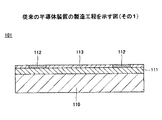
図1は、従来の半導体装置の断面図である。 FIG. 1 is a cross-sectional view of a conventional semiconductor device.
図1を参照するに、従来の半導体装置100(例えば、チップサイズパッケージ)は、半導体チップ101と、内部接続端子102と、樹脂層103と、配線パターン104と、ソルダーレジスト106と、外部接続端子107とを有する。
Referring to FIG. 1, a conventional semiconductor device 100 (for example, a chip size package) includes a
半導体チップ101は、薄板化された半導体基板110と、半導体集積回路111と、複数の電極パッド112と、保護膜113とを有する。半導体集積回路111は、半導体基板110の表面側に設けられている。半導体集積回路111は、拡散層、絶縁層、ビア、及び配線等から構成されている。複数の電極パッド112は、半導体集積回路111上に設けられている。複数の電極パッド112は、半導体集積回路111に設けられた配線と電気的に接続されている。保護膜113は、半導体集積回路111上に設けられている。保護膜113は、半導体集積回路111を保護するための膜である。
The
内部接続端子102は、電極パッド112上に設けられている。内部接続端子102の上端部の上面は、樹脂層103から露出されている。内部接続端子102の上端部は、配線パターン104と接続されている。樹脂層103は、内部接続端子102が設けられた側の半導体チップ101を覆うように設けられている。
The
配線パターン104は、樹脂層103上に設けられている。配線パターン104は、内部接続端子102と接続されている。配線パターン104は、内部接続端子102を介して、電極パッド112と電気的に接続されている。配線パターン104は、外部接続端子107が配設される外部接続端子配設領域104Aを有する。ソルダーレジスト106は、外部接続端子配設領域104A以外の配線パターン104部分を覆うように、樹脂層103上に設けられている。
The
図2〜図10は、従来の半導体装置の製造工程を示す図である。図2〜図10において、図1に示した従来の半導体装置100と同一構成部分には同一符号を付す。
2 to 10 are views showing a manufacturing process of a conventional semiconductor device. 2 to 10, the same components as those of the
始めに、図2に示す工程では、薄板化される前の半導体基板110の表面側に、半導体集積回路111、複数の電極パッド112、及び保護膜113を有した半導体チップ101を形成する。次いで、図3に示す工程では、複数の電極パッド112上に内部接続端子102を形成する。この段階では、複数の内部接続端子102には、高さのばらつきがある。
First, in the step shown in FIG. 2, the
次いで、図4に示す工程では、複数の内部接続端子102の上端部に平坦な板115を押し当てて、複数の内部接続端子102の高さを揃える。次いで、図5に示す工程では、内部接続端子102が形成された側の半導体チップ101及び内部接続端子102を覆うように樹脂層103を形成する。
Next, in the process shown in FIG. 4, the
次いで、図6に示す工程では、内部接続端子102の上端部の上面102Aが樹脂層103から露出するまで、樹脂層103を研磨する。このとき、樹脂層103の上面103Aが内部接続端子102の上端部の上面102Aと略面一となるように研磨を行う。
Next, in the step shown in FIG. 6, the
次いで、図7に示す工程では、樹脂層103の上面103Aに配線パターン104を形成する。次いで、図8に示す工程では、外部接続端子配設領域104A以外の部分の配線パターン104を覆うように、樹脂層103上にソルダーレジスト106を形成する。
Next, in the process shown in FIG. 7, the
次いで、図9に示す工程では、半導体基板110の裏面側から半導体基板110を研磨して、半導体基板110を薄板化する。次いで、図10に示す工程では、外部接続端子配設領域104Aに外部接続端子107を形成する。これにより、半導体装置100が製造される(例えば、特許文献1参照。)。
しかしながら、従来の半導体装置100の製造方法では、複数の内部接続端子102の高さを揃える工程や、樹脂層103を研磨して複数の内部接続端子102の上面102Aを樹脂層103から露出させる工程が必要であるため、工程数が増加して、半導体装置100の製造コストが増加してしまうという問題があった。
However, in the conventional method for manufacturing the
また、樹脂層103を研磨する場合、内部接続端子102の上端部の上面102Aに存在する樹脂層103を精度良く除去することが困難なため、内部接続端子102の上端部の上面102Aに樹脂層103が残ってしまう。これにより、内部接続端子102と配線パターン104との間の密着性が低下(最悪の場合、内部接続端子102と配線パターン104との間で剥がれが発生する)や、内部接続端子102と配線パターン104との間の抵抗値の増大等により、半導体装置100の歩留まりが低下してしまうという問題があった。
Further, when the
そこで本発明は、上述した問題点に鑑みなされたものであり、工程数を削減して、半導体装置の製造コストの低減を図ることができると共に、半導体装置の歩留まりを向上させることのできる半導体装置の製造方法を提供することを目的とする。 Therefore, the present invention has been made in view of the above-described problems, and can reduce the number of steps to reduce the manufacturing cost of the semiconductor device and improve the yield of the semiconductor device. It aims at providing the manufacturing method of.
本発明の一観点によれば、複数の半導体チップが形成される半導体基板と、電極パッドを有した前記複数の半導体チップと、前記電極パッドに設けられた内部接続端子と、前記内部接続端子と接続された配線パターンと、を備えた半導体装置の製造方法であって、前記内部接続端子が設けられた側の前記複数の半導体チップと前記内部接続端子とを覆うように絶縁層を形成する絶縁層形成工程と、前記絶縁層上に金属層を形成する金属層形成工程と、前記金属層の全体を押圧して、前記金属層と前記内部接続端子の上端部とを接触させる金属層押圧工程と、前記内部接続端子の上端部と接触する部分の前記金属層を押圧して、前記内部接続端子に第1の凹部を形成すると共に、前記金属層に第2の凹部を形成する凹部形成工程と、前記凹部形成工程後に、前記金属層をエッチングして前記配線パターンを形成する配線パターン形成工程と、を含むことを特徴とする半導体装置の製造方法が提供される。 According to one aspect of the present invention, a semiconductor substrate on which a plurality of semiconductor chips are formed, the plurality of semiconductor chips having electrode pads, internal connection terminals provided on the electrode pads, and the internal connection terminals A method of manufacturing a semiconductor device comprising a connected wiring pattern, wherein an insulating layer is formed so as to cover the plurality of semiconductor chips on the side where the internal connection terminals are provided and the internal connection terminals A layer forming step, a metal layer forming step of forming a metal layer on the insulating layer, and a metal layer pressing step of pressing the entire metal layer to bring the metal layer and the upper end portion of the internal connection terminal into contact with each other. And forming a first recess in the internal connection terminal and forming a second recess in the metal layer by pressing the portion of the metal layer in contact with the upper end portion of the internal connection terminal. And the concave shape After step method of manufacturing a semiconductor device which comprises a wiring pattern forming step of forming the wiring patterns by etching the metal layer is provided.
本発明によれば、内部接続端子が設けられた側の複数の半導体チップと内部接続端子とを覆うように絶縁層を形成し、次いで、絶縁層上に金属層を形成し、その後、金属層の全体を押圧して金属層と内部接続端子の上端部とを接触させることにより、従来、必要であった複数の内部接続端子の高さを揃える工程、及び複数の内部接続端子の一部を絶縁層から露出させるための絶縁層を研磨する工程が不要となるため、工程数を削減することが可能となるので、半導体装置の製造コストの低減を図ることができる。 According to the present invention, an insulating layer is formed so as to cover the plurality of semiconductor chips on the side where the internal connection terminals are provided and the internal connection terminals, and then a metal layer is formed on the insulating layer, and then the metal layer The step of aligning the heights of the plurality of internal connection terminals, which has conventionally been required, and a part of the plurality of internal connection terminals Since the step of polishing the insulating layer to be exposed from the insulating layer is not necessary, the number of steps can be reduced, and the manufacturing cost of the semiconductor device can be reduced.
また、金属層の全体を押圧して金属層と内部接続端子の上端部とを接触させた後、内部接続端子の上端部と接触する部分の金属層を押圧して、内部接続端子に第1の凹部を形成すると共に、金属層に第2の凹部を形成することにより、第1の凹部の底面及び側面と金属層とが接触するため、内部接続端子と配線パターンとの接触面積が増加する。これにより、内部接続端子と配線パターンとの間の密着性を向上できると共に、内部接続端子と配線パターンとの間に絶縁層が介在されにくくなる(絶縁層の影響により内部接続端子と配線パターンとの間の抵抗値が増加することがなくなる)ため、半導体装置の歩留まりを向上させることができる。 Further, after pressing the entire metal layer to bring the metal layer into contact with the upper end portion of the internal connection terminal, the metal layer in the portion in contact with the upper end portion of the internal connection terminal is pressed, and the first internal connection terminal is pressed. By forming the second concave portion and forming the second concave portion in the metal layer, the bottom and side surfaces of the first concave portion and the metal layer are in contact with each other, so that the contact area between the internal connection terminal and the wiring pattern increases. . As a result, the adhesion between the internal connection terminal and the wiring pattern can be improved, and an insulating layer is less likely to be interposed between the internal connection terminal and the wiring pattern. Therefore, the yield of the semiconductor device can be improved.
本発明の他の観点によれば、複数の半導体チップが形成される半導体基板と、電極パッドを有した前記複数の半導体チップと、前記電極パッドに設けられた内部接続端子と、前記内部接続端子と接続された配線パターンと、を備えた半導体装置の製造方法であって、前記内部接続端子が設けられた側の前記複数の半導体チップと前記内部接続端子とを覆うように絶縁層を形成する絶縁層形成工程と、前記絶縁層上に金属層を形成する金属層形成工程と、前記金属層の全体を押圧して、前記金属層と前記内部接続端子の上端部とを接触させる金属層押圧工程と、前記金属層をエッチングして前記配線パターンを形成する配線パターン形成工程と、前記内部接続端子の上端部と接触する部分の前記配線パターンを押圧して、前記内部接続端子に第1の凹部を形成すると共に、前記配線パターンに第2の凹部を形成する凹部形成工程と、を含むことを特徴とする半導体装置の製造方法が提供される。 According to another aspect of the present invention, a semiconductor substrate on which a plurality of semiconductor chips are formed, the plurality of semiconductor chips having electrode pads, internal connection terminals provided on the electrode pads, and the internal connection terminals A wiring pattern connected to the semiconductor device, wherein an insulating layer is formed so as to cover the plurality of semiconductor chips on the side where the internal connection terminals are provided and the internal connection terminals An insulating layer forming step, a metal layer forming step of forming a metal layer on the insulating layer, and a metal layer pressing that presses the entire metal layer to bring the metal layer into contact with the upper end portion of the internal connection terminal. A step of forming a wiring pattern by etching the metal layer, and pressing the wiring pattern at a portion in contact with the upper end portion of the internal connection terminal. To form a recess, a method of manufacturing a semiconductor device which comprises a a recess forming step of forming a second recess in the wiring pattern.
本発明によれば、内部接続端子が設けられた側の複数の半導体チップと内部接続端子とを覆うように絶縁層を形成し、次いで、絶縁層上に金属層を形成し、その後、金属層の全体を押圧して金属層と内部接続端子の上端部とを接触させることにより、従来、必要であった複数の内部接続端子の高さを揃える工程、及び複数の内部接続端子の一部を絶縁層から露出させるための絶縁層を研磨する工程が不要となるため、工程数を削減することが可能となるので、半導体装置の製造コストの低減を図ることができる。 According to the present invention, an insulating layer is formed so as to cover the plurality of semiconductor chips on the side where the internal connection terminals are provided and the internal connection terminals, and then a metal layer is formed on the insulating layer, and then the metal layer The step of aligning the heights of the plurality of internal connection terminals, which has conventionally been required, and a part of the plurality of internal connection terminals Since the step of polishing the insulating layer to be exposed from the insulating layer is not necessary, the number of steps can be reduced, and the manufacturing cost of the semiconductor device can be reduced.
また、金属層の全体を押圧して金属層と内部接続端子の上端部とを接触させた後、金属層をエッチングして配線パターンを形成し、その後、内部接続端子の上端部と接触する部分の配線パターンを押圧して、内部接続端子に第1の凹部を形成すると共に、配線パターンに第2の凹部を形成することにより、第1の凹部の底面及び側面と配線パターンとが接触するため、内部接続端子と配線パターンとの接触面積が増加する。これにより、内部接続端子と配線パターンとの間の密着性を向上できると共に、内部接続端子と配線パターンとの間に絶縁層が介在されにくくなる(絶縁層の影響により内部接続端子と配線パターンとの間の抵抗値が増加することがなくなる)ため、半導体装置の歩留まりを向上させることができる。 Also, after pressing the entire metal layer to bring the metal layer into contact with the upper end of the internal connection terminal, the metal layer is etched to form a wiring pattern, and then the portion that comes into contact with the upper end of the internal connection terminal By pressing the wiring pattern to form the first recess in the internal connection terminal and forming the second recess in the wiring pattern, the bottom and side surfaces of the first recess come into contact with the wiring pattern. The contact area between the internal connection terminal and the wiring pattern increases. As a result, the adhesion between the internal connection terminal and the wiring pattern can be improved, and an insulating layer is less likely to be interposed between the internal connection terminal and the wiring pattern. Therefore, the yield of the semiconductor device can be improved.
本発明のその他の観点によれば、複数の半導体チップが形成される半導体基板と、電極パッドを有した前記複数の半導体チップと、前記電極パッドに設けられた内部接続端子と、前記内部接続端子と接続された配線パターンと、を備えた半導体装置の製造方法であって、
前記内部接続端子が設けられた側の前記複数の半導体チップと前記内部接続端子とを覆うように絶縁層を形成する絶縁層形成工程と、前記絶縁層上に金属層を形成する金属層形成工程と、前記金属層の全体を押圧して、前記金属層と前記内部接続端子の上端部とを接触させる金属層押圧工程と、平面視において、前記金属層と接触している前記内部接続端子の上端部の周囲に位置する部分の前記金属層を押圧して、前記絶縁層に前記内部接続端子の上端部の外周面を露出する第1の凹部を形成すると共に、前記金属層に第2の凹部を形成する凹部形成工程と、前記凹部形成工程後に、前記金属層をエッチングして前記配線パターンを形成する配線パターン形成工程と、を含むことを特徴とする半導体装置の製造方法が提供される。
According to another aspect of the present invention, a semiconductor substrate on which a plurality of semiconductor chips are formed, the plurality of semiconductor chips having electrode pads, internal connection terminals provided on the electrode pads, and the internal connection terminals A method of manufacturing a semiconductor device comprising a wiring pattern connected to
An insulating layer forming step of forming an insulating layer so as to cover the plurality of semiconductor chips on the side where the internal connecting terminals are provided and the internal connecting terminals, and a metal layer forming step of forming a metal layer on the insulating layer And a metal layer pressing step of pressing the entire metal layer to bring the metal layer into contact with the upper end of the internal connection terminal, and in plan view, the internal connection terminal in contact with the metal layer A portion of the metal layer located around the upper end is pressed to form a first recess exposing the outer peripheral surface of the upper end of the internal connection terminal in the insulating layer, and a second recess is formed in the metal layer. There is provided a method for manufacturing a semiconductor device, comprising: a recess forming step for forming a recess; and a wiring pattern forming step for forming the wiring pattern by etching the metal layer after the recess forming step. .
本発明によれば、内部接続端子が設けられた側の複数の半導体チップと内部接続端子とを覆うように絶縁層を形成し、次いで、絶縁層上に金属層を形成し、その後、金属層の全体を押圧して金属層と内部接続端子の上端部とを接触させることにより、従来、必要であった複数の内部接続端子の高さを揃える工程、及び複数の内部接続端子の一部を絶縁層から露出させるための絶縁層を研磨する工程が不要となるため、工程数を削減することが可能となるので、半導体装置の製造コストの低減を図ることができる。 According to the present invention, an insulating layer is formed so as to cover the plurality of semiconductor chips on the side where the internal connection terminals are provided and the internal connection terminals, and then a metal layer is formed on the insulating layer, and then the metal layer The step of aligning the heights of the plurality of internal connection terminals, which has conventionally been required, and a part of the plurality of internal connection terminals Since the step of polishing the insulating layer to be exposed from the insulating layer is not necessary, the number of steps can be reduced, and the manufacturing cost of the semiconductor device can be reduced.
また、金属層の全体を押圧して金属層と内部接続端子の上端部とを接触させた後、内部接続端子の上端部の外周部に配置された部分の金属層を押圧して、絶縁層に内部接続端子の上端部の外周面を露出する第1の凹部を形成すると共に、金属層に第2の凹部を形成することにより、内部接続端子の上端部の外周面と金属層とが接触して、内部接続端子と金属層との接触面積が増加するため、内部接続端子と配線パターンとの間の密着性を向上させることができると共に、内部接続端子と配線パターンとの間に絶縁層が介在されにくくなる(絶縁層の影響により内部接続端子と配線パターンとの間の抵抗値が増加することがなくなる)ため、半導体装置の歩留まりを向上させることができる。 Also, after pressing the entire metal layer to bring the metal layer into contact with the upper end portion of the internal connection terminal, the metal layer at the outer peripheral portion of the upper end portion of the internal connection terminal is pressed to form an insulating layer Forming a first recess that exposes the outer peripheral surface of the upper end portion of the internal connection terminal, and forming a second recess in the metal layer so that the outer peripheral surface of the upper end portion of the internal connection terminal and the metal layer are in contact with each other. Since the contact area between the internal connection terminal and the metal layer is increased, the adhesion between the internal connection terminal and the wiring pattern can be improved, and the insulating layer is provided between the internal connection terminal and the wiring pattern. Since the resistance value between the internal connection terminal and the wiring pattern does not increase due to the influence of the insulating layer, the yield of the semiconductor device can be improved.
本発明のその他の観点によれば、複数の半導体チップが形成される半導体基板と、電極パッドを有した前記複数の半導体チップと、前記電極パッドに設けられた内部接続端子と、前記内部接続端子と接続された配線パターンと、を備えた半導体装置の製造方法であって、前記内部接続端子が設けられた側の前記複数の半導体チップと前記内部接続端子とを覆うように絶縁層を形成する絶縁層形成工程と、前記絶縁層上に金属層を形成する金属層形成工程と、前記金属層の全体を所定の圧力で押圧して、前記金属層と前記内部接続端子の上端部とを接触させる金属層押圧工程と、前記金属層をエッチングして前記配線パターンを形成する配線パターン形成工程と、平面視において、前記配線パターンと接触している前記内部接続端子の上端部の周囲に位置する部分の前記配線パターンを押圧して、前記絶縁層に前記内部接続端子の上端部の外周面を露出する第1の凹部を形成すると共に、前記配線パターンに第2の凹部を形成する凹部形成工程と、を含むことを特徴とする半導体装置の製造方法が提供される。 According to another aspect of the present invention, a semiconductor substrate on which a plurality of semiconductor chips are formed, the plurality of semiconductor chips having electrode pads, internal connection terminals provided on the electrode pads, and the internal connection terminals A wiring pattern connected to the semiconductor device, wherein an insulating layer is formed so as to cover the plurality of semiconductor chips on the side where the internal connection terminals are provided and the internal connection terminals An insulating layer forming step, a metal layer forming step of forming a metal layer on the insulating layer, and pressing the entire metal layer with a predetermined pressure to bring the metal layer into contact with the upper end portion of the internal connection terminal a metal layer pushing step of a wiring pattern forming step of forming the wiring patterns by etching the metal layer in a plan view, the upper end of the internal connecting terminal in contact with the wiring pattern By pressing the wiring pattern of the portion located on the circumference, to form a first recess exposing the outer peripheral surface of the upper portion of the internal connection terminals to said insulating layer, forming a second recess in the wiring pattern And a recess forming step. The method for manufacturing a semiconductor device is provided.
本発明によれば、内部接続端子が設けられた側の複数の半導体チップと内部接続端子とを覆うように絶縁層を形成し、次いで、絶縁層上に金属層を形成し、その後、金属層の全体を押圧して金属層と内部接続端子の上端部とを接触させることにより、従来、必要であった複数の内部接続端子の高さを揃える工程、及び複数の内部接続端子の一部を絶縁層から露出させるための絶縁層を研磨する工程が不要となるため、工程数を削減することが可能となるので、半導体装置の製造コストの低減を図ることができる。 According to the present invention, an insulating layer is formed so as to cover the plurality of semiconductor chips on the side where the internal connection terminals are provided and the internal connection terminals, and then a metal layer is formed on the insulating layer, and then the metal layer The step of aligning the heights of the plurality of internal connection terminals, which has conventionally been required, and a part of the plurality of internal connection terminals Since the step of polishing the insulating layer to be exposed from the insulating layer is not necessary, the number of steps can be reduced, and the manufacturing cost of the semiconductor device can be reduced.
また、金属層の全体を押圧して金属層と内部接続端子の上端部とを接触させた後、金属層をエッチングして配線パターンを形成し、その後、内部接続端子の上端部の外周部に配置された部分の配線パターンを押圧して、絶縁層に内部接続端子の上端部の外周面を露出する第1の凹部を形成すると共に、配線パターンに第2の凹部を形成することにより、内部接続端子の上端部の外周面と配線パターンとが接触して、内部接続端子と配線パターンとの接触面積が増加するため、内部接続端子と配線パターンとの間の密着性を向上させることができると共に、内部接続端子と配線パターンとの間に絶縁層が介在されにくくなる(絶縁層の影響により内部接続端子と配線パターンとの間の抵抗値が増加することがなくなる)ため、半導体装置の歩留まりを向上させることができる。
本発明のその他の観点によれば、半導体チップと、前記半導体チップと接続された内部接続端子と、前記内部接続端子の部分を除いて半導体チップを覆うように形成された絶縁層と、前記絶縁層上に設けられ、前記内部接続端子と接続された配線パターンと、前記配線パターンに接続された外部接続端子と、前記配線パターン及び前記絶縁層を覆い、前記配線パターンと前記外部接続端子との接続部を露出する開口部を有するソルダーレジストと、を備えた半導体装置であって、前記内部接続端子は、前記配線パターン側に設けられた第1の凹部を有し、前記配線パターンの前記ソルダーレジスト側には、平面視において前記第1の凹部と重複する領域内に、前記第1の凹部よりも平面形状が小さく、前記第1の凹部に対応する深さの第2の凹部が設けられ、前記内部接続端子は、前記絶縁層から露出する上面と、前記第1の凹部の側面及び底面とが、前記配線パターンに接触されていることを特徴とする半導体装置が提供される。
本発明によれば、配線パターンと半導体チップとを電気的に接続する内部接続端子に凹部を設けると共に、凹部上に配置された部分の配線パターンに凹部を設けて、凹部の形成領域に対応する部分の配線パターンを凹部の側面及び底面と接触させることにより、内部接続端子と配線パターンとの接触面積が大きくなるため、内部接続端子と配線パターンとの間の抵抗値を小さくすることが可能となるので、半導体装置の歩留まりを向上できる。
本発明のその他の観点によれば、半導体チップと、前記半導体チップと接続された内部接続端子と、前記内部接続端子の部分を除いて半導体チップを覆うように形成された絶縁層と、前記絶縁層上に設けられ、前記内部接続端子と接続された配線パターンと、前記配線パターンに接続された外部接続端子と、前記配線パターン及び前記絶縁層を覆い、前記配線パターンと前記外部接続端子との接続部を露出する開口部を有するソルダーレジストと、を備えた半導体装置であって、前記内部接続端子は、前記配線パターン側に突起した凸形状であり、前記絶縁層は、前記内部接続端子の前記絶縁層から露出する上面の外周の側面部及び平面視において前記上面の周囲に位置する面が露出するように、前記外周に第1の凹部を有し、前記配線パターンの前記ソルダーレジスト側には、平面視において前記第1の凹部と重複する領域内に、前記第1の凹部よりも平面形状が小さく、前記第1の凹部に対応する深さの第2の凹部が設けられ、前記内部接続端子は、前記絶縁層から露出する上面と、前記絶縁層から露出する前記外周の側面部と、前記上面の周囲に位置する面とが、前記配線パターンに接触されていることを特徴とする半導体装置が提供される。
本発明によれば、内部接続端子の上端部の上面と配線パターンとを接触させると共に、絶縁層に内部接続端子の上端部の外周側面を露出するリング状の凹部を設け、凹部の上方に配置された部分の配線パターンにリング状の凹部を設けて、凹部に配置された部分の配線パターンにより内部接続端子の上端部の外周側面を覆うことにより、内部接続端子と配線パターンとの接触面積が増加するため、内部接続端子と配線パターンとの間の密着性を向上させることができると共に、内部接続端子と配線パターンとの間に絶縁層が介在されにくくなる(絶縁層の影響により内部接続端子と配線パターンとの間の抵抗値が増加することがなくなる)ため、半導体装置の歩留まりを向上させることができる。
Also, after pressing the entire metal layer to bring the metal layer into contact with the upper end of the internal connection terminal, the metal layer is etched to form a wiring pattern, and then on the outer periphery of the upper end of the internal connection terminal. By pressing the wiring pattern of the arranged portion to form a first recess that exposes the outer peripheral surface of the upper end portion of the internal connection terminal in the insulating layer, and by forming a second recess in the wiring pattern, Since the outer peripheral surface of the upper end portion of the connection terminal and the wiring pattern come into contact with each other and the contact area between the internal connection terminal and the wiring pattern increases, the adhesion between the internal connection terminal and the wiring pattern can be improved. At the same time, the insulating layer is less likely to be interposed between the internal connection terminal and the wiring pattern (the resistance value between the internal connection terminal and the wiring pattern is not increased due to the influence of the insulating layer). Stay Ri can be improved.
According to another aspect of the present invention, a semiconductor chip, an internal connection terminal connected to the semiconductor chip, an insulating layer formed to cover the semiconductor chip except for the portion of the internal connection terminal, and the insulation A wiring pattern provided on the layer and connected to the internal connection terminal; an external connection terminal connected to the wiring pattern; the wiring pattern and the insulating layer; and the wiring pattern and the external connection terminal A solder resist having an opening that exposes the connection portion, wherein the internal connection terminal has a first recess provided on the wiring pattern side, and the solder of the wiring pattern On the resist side, in a region overlapping with the first concave portion in plan view, the planar shape is smaller than the first concave portion and has a depth corresponding to the first concave portion. A semiconductor device is provided, wherein the internal connection terminal has a top surface exposed from the insulating layer and a side surface and a bottom surface of the first recess in contact with the wiring pattern. The
According to the present invention, the internal connection terminal that electrically connects the wiring pattern and the semiconductor chip is provided with the recess, and the recess is provided in the wiring pattern of the portion disposed on the recess to correspond to the formation area of the recess. Since the contact area between the internal connection terminal and the wiring pattern is increased by bringing the partial wiring pattern into contact with the side surface and bottom surface of the recess, the resistance value between the internal connection terminal and the wiring pattern can be reduced. Therefore, the yield of the semiconductor device can be improved.
According to another aspect of the present invention, a semiconductor chip, an internal connection terminal connected to the semiconductor chip, an insulating layer formed to cover the semiconductor chip except for the portion of the internal connection terminal, and the insulation A wiring pattern provided on the layer and connected to the internal connection terminal; an external connection terminal connected to the wiring pattern; the wiring pattern and the insulating layer; and the wiring pattern and the external connection terminal A solder resist having an opening that exposes the connection portion, wherein the internal connection terminal has a convex shape protruding toward the wiring pattern, and the insulating layer is formed of the internal connection terminal. The wiring pattern has a first recess on the outer periphery so that a side surface portion of the outer periphery of the upper surface exposed from the insulating layer and a surface located around the upper surface in a plan view are exposed. On the side of the solder resist in a plane, in a region overlapping with the first recess in plan view, the planar shape is smaller than the first recess and has a depth corresponding to the first recess. A recess is provided, and the internal connection terminal has an upper surface exposed from the insulating layer, a side surface portion of the outer periphery exposed from the insulating layer, and a surface located around the upper surface in contact with the wiring pattern. A semiconductor device is provided.
According to the present invention, the upper surface of the upper end of the internal connection terminal is brought into contact with the wiring pattern, and the insulating layer is provided with the ring-shaped recess that exposes the outer peripheral side surface of the upper end of the internal connection terminal, and is disposed above the recess By providing a ring-shaped recess in the wiring pattern of the part, and covering the outer peripheral side surface of the upper end portion of the internal connection terminal with the wiring pattern of the part arranged in the recess, the contact area between the internal connection terminal and the wiring pattern is increased. Therefore, the adhesion between the internal connection terminal and the wiring pattern can be improved, and an insulating layer is less likely to be interposed between the internal connection terminal and the wiring pattern (the internal connection terminal is affected by the influence of the insulating layer). The resistance value between the wiring pattern and the wiring pattern is not increased), and the yield of the semiconductor device can be improved.
本発明によれば、工程数を削減して、半導体装置の製造コストの低減を図ることができると共に、半導体装置の歩留まりを向上させることができる。 According to the present invention, the number of steps can be reduced to reduce the manufacturing cost of the semiconductor device, and the yield of the semiconductor device can be improved.
次に、図面に基づいて本発明の実施の形態について説明する。 Next, embodiments of the present invention will be described with reference to the drawings.
(第1の実施の形態)
図11は、本発明の第1の実施の形態に係る半導体装置の断面図である。
(First embodiment)
FIG. 11 is a cross-sectional view of the semiconductor device according to the first embodiment of the present invention.
図11を参照するに、第1の実施の形態の半導体装置10は、半導体チップ11と、内部接続端子12と、絶縁層13と、配線パターン14,15と、ソルダーレジスト16と、外部接続端子17とを有する。
Referring to FIG. 11, the
半導体チップ11は、半導体基板21と、半導体集積回路22と、電極パッド23と、保護膜24とを有する。半導体基板21は、半導体集積回路22を形成するための基板である。半導体基板21は、薄板化されている。半導体基板21の厚さT1は、例えば、100μm〜300μmとすることができる。半導体基板21としては、例えば、シリコン基板(具体的には、薄板化されたシリコンウエハを個片化したもの)を用いることができる。
The
半導体集積回路22は、半導体基板21の上面21A側に設けられている。半導体集積回路22は、半導体基板21に形成された拡散層(図示せず)、半導体基板21上に積層された絶縁層(図示せず)、積層された絶縁層に設けられたビア(図示せず)、及び配線等(図示せず)から構成されている。
The semiconductor integrated
電極パッド23は、半導体集積回路22上に複数設けられている。電極パッド23は、半導体集積回路22に設けられた配線(図示せず)と電気的に接続されている。電極パッド23の材料としては、例えば、AlやAlを含んだ合金(例えば、Al−Si−Cu合金)を用いることができる。
A plurality of
保護膜24は、半導体集積回路22上に設けられている。保護膜24は、半導体集積回路22を保護するための膜である。保護膜24としては、例えば、SiN膜やPSG膜等を用いることができる。
The
内部接続端子12は、電極パッド23上に設けられている。内部接続端子12の下端部は、電極パッド23を介して、半導体集積回路22と電気的に接続されている。内部接続端子12の上端部12−1は、配線パターン14と対向する部分に第1の凹部である凹部12−1Aを有する。凹部12−1Aの側面及び底面と内部接続端子12の上端部12−1の上面とは、配線パターン14と接触している。これにより、配線14と半導体集積回路22とは、内部接続端子12により電気的に接続されている。内部接続端子12の上端部12−1の直径が40μmの場合、凹部12−1Aの直径は、例えば、20μmとすることができる。この場合、凹部12−1Aの深さは、例えば、10μmとすることができる。
The
内部接続端子12の高さH1は、絶縁層13の厚さT2と略等しい。内部接続端子12の高さH1は、例えば、10μm〜60μmとすることができる。内部接続端子12としては、例えば、Auバンプ、Auめっき膜、無電解めっき法により形成されたNi膜とそれを覆うAu膜から構成される金属膜等を用いることができる。Auバンプは、例えば、ボンディング法やめっき法により形成することができる。
The height H 1 of the
絶縁層13は、内部接続端子12の上端部12−1の上面及び凹部12−1Aを除いた部分の内部接続端子12と半導体チップ11上とを覆うように設けられている。絶縁層13としては、例えば、粘着性を有したシート状の絶縁樹脂(例えば、NCF(Non Conductive Film))、ペースト状の絶縁樹脂(例えば、NCP(Non Conductive Paste))、異方性導電樹脂(例えば、ACF(Anisotropic Conductive Film))等を用いることができる。絶縁層13の厚さT2は、例えば、10μm〜60μmとすることができる。
The insulating
配線パターン14は、内部接続端子12の上端部12−1及びその近傍に配置された絶縁層13上に設けられている。配線パターン14は、接続部14Aと、第2の凹部である凹部14Bとを有する。接続部14Aは、絶縁層13上に配置されている。接続部14Aには、外部接続端子17が配設されている。
The
凹部14Bは、内部接続端子12の凹部12−1A上に配置された部分の配線パターン14に形成されている。凹部14Bの形成領域に対応する部分の配線パターン14は、内部接続端子12の凹部12−1Aの側面及び底面と接触している。上記構成とされた配線パターン14は、内部接続端子12を介して、半導体集積回路22と電気的に接続されている。
The
このように、内部接続端子12に凹部12−1Aを設けると共に、凹部12−1A上に配置された部分の配線パターン14に凹部14Bを設けて、凹部14Bの形成領域に対応する部分の配線パターン14を凹部12−1Aの側面及び底面と接触させることにより、内部接続端子12と配線パターン14との接触面積が大きくなるため、内部接続端子12と配線パターン14との間の抵抗値を小さくすることができる。
As described above, the recess 12-1A is provided in the
配線パターン14としては、例えば、Cu膜を用いることができる。この場合、配線パターン14と外部接続端子17との間に、図示していない拡散防止膜を形成するとよい。拡散防止膜としては、例えば、配線パターン14上に、Ni層と、Au層とを順次積層させたNi/Au積層膜を用いることができる。配線パターン14としてCu膜を用いた場合、配線パターン14の厚さは、例えば、12μmとすることができる。
As the
配線パターン15は、絶縁層13の上面13Aに設けられている。配線パターン15は、接続部15Aを有する。接続部15Aには、外部接続端子17が配設されている。配線パターン15としては、例えば、Cu膜を用いることができる。この場合、配線パターン15と外部接続端子17との間に、図示していない拡散防止膜を形成するとよい。拡散防止膜としては、例えば、配線パターン15上に、Ni層と、Au層とを順次積層させたNi/Au積層膜を用いることができる。配線パターン15としてCu膜を用いた場合、配線パターン15の厚さは、例えば、12μmとすることができる。
The
ソルダーレジスト16は、接続部14A,15Aを除いた部分の配線パターン14,15を覆うように絶縁層13上に設けられている。ソルダーレジスト16は、接続部14Aを露出する開口部16Aと、接続部15Aを露出する開口部16Bとを有する。
The solder resist 16 is provided on the insulating
外部接続端子17は、配線パターン14,15の接続部14A,15Aにそれぞれ配設されている。外部接続端子17は、マザーボード等の実装基板(図示せず)に設けられたパッドと電気的に接続される端子である。外部接続端子17としては、例えば、はんだバンプを用いることができる。
The
本実施の形態の半導体装置によれば、配線パターン14と半導体チップ11とを電気的に接続する内部接続端子12に凹部12−1Aを設けると共に、凹部12−1A上に配置された部分の配線パターン14に凹部14Bを設けて、凹部14Bの形成領域に対応する部分の配線パターン14を凹部12−1Aの側面及び底面と接触させることにより、内部接続端子12と配線パターン14との接触面積が大きくなるため、内部接続端子12と配線パターン14との間の抵抗値を小さくすることが可能となるので、半導体装置10の歩留まりを向上できる。
According to the semiconductor device of the present embodiment, the recess 12-1A is provided in the
図12〜図22は、本発明の第1の実施の形態に係る半導体装置の製造工程を示す図である。図12〜図22において、第1の実施の形態の半導体装置10と同一構成部分には同一符号を付す。また、図12〜図22において、Bはダイサーが半導体基板31を切断する位置(以下、「切断位置B」とする)を示している。
12 to 22 are views showing manufacturing steps of the semiconductor device according to the first embodiment of the present invention. 12 to 22, the same components as those of the
始めに、図12に示す工程では、複数の半導体装置形成領域Aを有した半導体基板31の上面31A側に、周知の手法により、半導体集積回路22、電極パッド23、及び保護膜24を有した半導体チップ11を形成する。半導体装置形成領域Aは、半導体装置10が形成される領域である。半導体基板31は、後述する工程において、薄板化され、かつ切断位置Bにおいて切断されることにより、先に説明した半導体基板21(図11参照)となるものである。
First, in the process shown in FIG. 12, the semiconductor integrated
半導体基板31としては、例えば、シリコンウエハを用いることができる。半導体基板31としてシリコンウエハを用いた場合、半導体基板31の厚さT3は、例えば、500μm〜775μmとすることができる。電極パッド23の材料としては、例えば、AlやAlを含んだ合金(例えば、Al−Si−Cu合金)を用いることができる。保護膜24としては、例えば、SiN膜やPSG膜等を用いることができる。
As the
次いで、図13に示す工程では、図12に示す構造体の複数の電極パッド23上にそれぞれ内部接続端子12を形成する。内部接続端子12としては、例えば、Auバンプ、Auめっき膜、無電解めっき法により形成されたNi膜とそれを覆うAu膜から構成される金属膜等を用いることができる。Auバンプは、例えば、ボンディング法により形成することができる。なお、図13に示す工程で形成された複数の内部接続端子12には、高さばらつきが存在する。
Next, in the step shown in FIG. 13, the
次いで、図14に示す工程では、内部接続端子12が設けられた側の複数の半導体チップ11及び複数の内部接続端子12を覆うように絶縁層13を形成する(絶縁層形成工程)。絶縁層13としては、粘着性を有したシート状の絶縁樹脂(例えば、NCF(Non Conductive Film))、ペースト状の絶縁樹脂(例えば、NCP(Non Conductive Paste))、異方性導電樹脂(例えば、ACF(Anisotropic Conductive Film))等を用いることができる。粘着性を有したシート状の絶縁樹脂を用いた場合は、図13に示す構造体の上面側にシート状の絶縁樹脂を貼り付けることで絶縁層13を形成する。また、絶縁層13としてペースト状の絶縁樹脂を用いた場合は、図13に示す構造体の上面側に印刷法によりペースト状の絶縁樹脂を形成し、その後、プリベークして絶縁樹脂を半硬化させる。この半硬化した絶縁樹脂は、接着性を有する。絶縁層13の厚さT4は、例えば、20μm〜100μmとすることができる。
Next, in a step shown in FIG. 14, an insulating
次いで、図15に示す工程では、絶縁層13の上面13Aに金属層33を形成する(金属層形成工程)。具体的には、例えば、金属層33としてCu箔を用意し、このCu箔を絶縁層13の上面13Aに貼り付ける。金属層33の厚さT5は、例えば、12μmとすることができる。金属層33は、後述する図17に示す工程において、エッチングされることにより配線パターン14,15となる。
Next, in a step shown in FIG. 15, a
次いで、図16に示す工程では、図15に示す構造体を加熱した状態で、金属層33の上面33Aに平板34を配置し、この平板34を介して、金属層33全体を押圧して、金属層33の下面33Bと複数の内部接続端子12の上端部12−1とを接触させることにより、複数の内部接続端子12の上端部12−1に略平坦とされた接触面12Aを形成する(金属層押圧工程)。
Next, in the step shown in FIG. 16, with the structure shown in FIG. 15 heated, a
複数の内部接続端子12の上端部12−1に略平坦とされた接触面12Aを形成後、金属層33から平板34を除去する。金属層33を押圧するときの圧力としては、例えば、4MPa(30mN/cm2)を用いることができる。金属層押圧工程後の絶縁層13の厚さT2は、例えば、10μm〜60μmとすることができる。また、内部接続端子12の高さH1は、絶縁層13の厚さT2と略等しく、具体的には、例えば、30μmとすることができる。
After forming a substantially
このように、金属層33の全体を押圧して金属層33の下面33Bと複数の内部接続端子12の上端部12−1とを接触させて、複数の内部接続端子12の上端部12−1に略平坦とされた接触面12Aを形成することにより、従来行われていた複数の内部接続端子12の高さを揃える工程、及び複数の内部接続端子12の上端部12−1の接触面12Aを絶縁層13から露出させるための研磨工程が不要となるため、製造工程数を削減することが可能となるので、半導体装置10の製造コストの低減を図ることができる。
In this way, the
次いで、図17に示す工程では、突出部37を有したプレス用工具36を準備し、図16に示す構造体を加熱した状態で、内部接続端子12の上端部12−1上に配置された部分の金属層33に突出部37を当接させた後、突出部37により、内部接続端子12の上端部12−1上に配置された部分の金属層33を押圧(例えば、10gf〜30gf)することで、内部接続端子12に第1の凹部である凹部12−1Aを形成すると共に、金属層33に第2の凹部である凹部14Bを形成する(凹部形成工程)。
Next, in the step shown in FIG. 17, a
これにより、凹部14Bに対応する部分の金属層33は、内部接続端子12の凹部12−1Aの側面及び底面と接触するため、凹部形成工程における金属層33と内部接続端子12の上端部12−1との接触面積を、金属層押圧工程における金属層33と内部接続端子12の上端部12−1との接触面積よりも大きくすることができる。突出部37の形状としては、例えば、円柱や四角柱等を用いることができる。また、内部接続端子12の高さH1が30μmの場合、突出部37の突出量Cは、例えば、10μmとすることができる。
As a result, the
このように、金属層33の全体を押圧して金属層33と内部接続端子12の上端部12−1の接触面12Aとを接触させた後、内部接続端子12の上端部と接触する部分の金属層33を押圧して、内部接続端子12に凹部12−1Aを形成すると共に、金属層33に凹部14Bを形成することにより、内部接続端子12に形成された凹部12−1Aの底面及び側面と金属層33とが接触するため、内部接続端子12と配線パターン14との接触面積が増加する。これにより、内部接続端子12と配線パターン14との間の密着性を向上できると共に、内部接続端子12と配線パターン14との間に絶縁層13が介在されにくくなる(絶縁層13の影響により内部接続端子12と配線パターン14との間の抵抗値が増加することがなくなる)ため、半導体装置10の歩留まりを向上させることができる。
Thus, after pressing the
次いで、図18に示す工程では、図17に示す金属層33をエッチングして、配線パターン14,15を形成する(配線パターン形成工程)。具体的には、例えば、図17に示す金属層33上にパターニングされたレジスト膜(図示せず)を形成し、その後、このレジスト膜をマスクとするエッチング(例えば、ドライエッチング又はウエットエッチング)により、金属層33をエッチングして、配線パターン14,15を形成する。
Next, in the step shown in FIG. 18, the
次いで、図19に示す工程では、絶縁膜13上に、接続部14A,15Aを除いた部分の配線パターン14,15を覆うように、開口部16A,16Bを有したソルダーレジスト16を形成する。開口部16Aは、配線パターン14の接続部14Aを露出するように形成し、開口部16Bは、配線パターン15の接続部15Aを露出するように形成する。
Next, in a step shown in FIG. 19, a solder resist 16 having
次いで、図20に示す工程では、配線パターン14,15の接続部14A,15Aに外部接続端子17を形成する。外部接続端子17としては、例えば、はんだバンプを用いることができる。
Next, in the step shown in FIG. 20, the
次いで、図21に示す工程では、図20に示す半導体基板31の下面31B側から半導体基板31を研磨又は研削して、半導体基板31を薄板化する。半導体基板31の薄板化には、例えば、バックサイドグラインダーを用いることができる。薄板化後の半導体基板31の厚さT1は、例えば、100μm〜300μmとすることができる。これにより各半導体装置形成領域Aに半導体装置10に相当する構造体が形成される。
Next, in the step shown in FIG. 21, the
次いで、図22に示す工程では、図21に示す構造体を切断位置Bに沿って切断して、複数の半導体装置10を個片化する。これにより、複数の半導体装置10が製造される。
Next, in the step shown in FIG. 22, the structure shown in FIG. 21 is cut along the cutting position B to divide the plurality of
本実施の形態の半導体装置の製造方法によれば、金属層33全体を押圧して金属層33の下面33Bと複数の内部接続端子12の上端部12−1とを接触させて、複数の内部接続端子12の上端部12−1に略平坦とされた接触面12Aを形成することにより、従来行われていた複数の内部接続端子12の高さを揃える工程、及び複数の内部接続端子12の上端部12−1の接触面12Aを絶縁層13から露出させるための研磨工程が不要となるため、半導体装置10の製造工程数を削減することが可能となるので、半導体装置10の製造コストの低減を図ることができる。
According to the method for manufacturing a semiconductor device of the present embodiment, the
また、金属層33の全体を押圧して金属層33と内部接続端子12の上端部とを接触させた後、内部接続端子12の上端部12−1と接触する部分の金属層33を押圧して、内部接続端子12に凹部12−1Aを形成すると共に、金属層33に凹部14Bを形成することにより、内部接続端子12に形成された凹部12−1Aの底面及び側面に金属層33が接触するため、内部接続端子12と配線パターン14との接触面積が増加する。これにより、内部接続端子12と配線パターン14との間の密着性を向上できると共に、内部接続端子12と配線パターン14との間に絶縁層13が介在されにくくなる(絶縁層13の影響により内部接続端子12と配線パターン14との間の抵抗値が増加することがなくなる)ため、半導体装置10の歩留まりを向上させることができる。
Moreover, after pressing the
なお、本実施の形態では、凹部12−1A,14Bを形成後に、金属層33をエッチングして配線パターン14,15を形成した場合を例に挙げて説明したが、図16に示す金属層押圧工程後に金属層33をエッチングして配線パターン14,15を形成し、その後、凹部12−1A,凹部14Bを形成してもよい。
In the present embodiment, the case where the
図23は、他のプレス用工具の断面図であり、図24は、図23に示すプレス用工具により形成される凹部の断面形状を示す図である。 FIG. 23 is a cross-sectional view of another press tool, and FIG. 24 is a view showing a cross-sectional shape of a recess formed by the press tool shown in FIG.
図17に示す工程において使用したプレス用工具36の代わりに、図23に示す断面形状が台形とされた突出部42を有したプレス用工具41を用いて、凹部形成工程を行ってもよい。この場合、図24に示すように、内部接続端子12の上端部12−1に凹部12−1B(凹部12−1Bの底面からその上方に離間するにつれて幅広形状とされている)が形成されると共に、配線パターン14に凹部14C(凹部14Cの底面からその上方に離間するにつれて幅広形状とされている)が形成される。
Instead of the
図25は、その他のプレス用工具の断面図であり、図26は、図25に示すプレス用工具により形成される凹部の断面形状を示す図である。 25 is a cross-sectional view of another press tool, and FIG. 26 is a view showing a cross-sectional shape of a recess formed by the press tool shown in FIG.
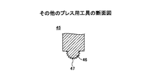
また、図17に示す工程において使用したプレス用工具36の代わりに、図25に示す複数の突起47を有した突出部46を有したプレス用工具45を用いて、凹部形成工程を行ってもよい。この場合、図26に示すように、内部接続端子12の上端部12−1に複数の突起47の形状が転写された凹部12−1Cが形成されると共に、配線パターン14に複数の突起47の形状が転写された凹部14Dが形成される。
Further, in place of the
このように、複数の突起47を有した突出部46を有したプレス用工具45を用いて凹部形成工程を行うことにより、配線パターン14と内部接続端子12との接触面積をさらに増加させることができる。突起47の高さは、例えば、5μmとすることができる。
Thus, the contact area between the
(第2の実施の形態)
図27は、本発明の第2の実施の形態に係る半導体装置の断面図である。図27において、第1の実施の形態の半導体装置10と同一構成部分には同一符号を付す。
(Second Embodiment)
FIG. 27 is a cross-sectional view of a semiconductor device according to the second embodiment of the present invention. In FIG. 27, the same components as those of the
図27を参照するに、第2の実施の形態の半導体装置50は、第1の実施の形態の半導体装置10に設けられた内部接続端子12の代わりに内部接続端子51を備えると共に、絶縁層13に凹部13Cを設け、さらに配線パターン14に設けられた凹部14Bの代わりに凹部14Eを設けた以外は半導体装置10と同様に構成される。
Referring to FIG. 27, the
内部接続端子51は、上面51−1Aが略平坦な面とされた上端部51−1を有する。上端部51−1の上面51−1Aは、絶縁層13の上面13Aと略面一とされており、配線パターン14と接触している。内部接続端子51の高さH2は、絶縁層13の厚さT2と略等しい。内部接続端子51の高さH2は、例えば、10μm〜60μmとすることができる。内部接続端子51としては、例えば、Auバンプ、Auめっき膜、無電解めっき法により形成されたNi膜とそれを覆うAu膜から構成される金属膜等を用いることができる。Auバンプは、例えば、ボンディング法やめっき法により形成することができる。
The
凹部13Cは、リング状の溝であり、内部接続端子51の上端部51−1の外周部に配置された部分の絶縁層13に形成されている。凹部13Cは、内部接続端子51の上端部51−1の外周側面を露出するように形成されている。凹部13Cの深さは、例えば、15μmとすることができる。
The
凹部14Eは、リング状の溝であり、凹部13Cの上方に配置された部分の配線パターン14に形成されている。凹部14Eに対応する部分の配線パターン14は、内部接続端子51の上端部51−1の外周側面を覆うように配置されている。
The
本実施の形態の半導体装置によれば、内部接続端子51の上端部51−1の上面51−1Aと配線パターン14とを接触させると共に、絶縁層13に内部接続端子51の上端部51−1の外周側面を露出するリング状の凹部13Cを設け、凹部13Cの上方に配置された部分の配線パターン14にリング状の凹部14Eを設けて、凹部13Cに配置された部分の配線パターン14により内部接続端子51の上端部51−1の外周側面を覆うことにより、内部接続端子51と配線パターン14との接触面積が増加するため、内部接続端子51と配線パターン14との間の密着性を向上させることができると共に、内部接続端子51と配線パターン14との間に絶縁層13が介在されにくくなる(絶縁層13の影響により内部接続端子51と配線パターン14との間の抵抗値が増加することがなくなる)ため、半導体装置50の歩留まりを向上させることができる。
According to the semiconductor device of the present embodiment, the upper surface 51-1A of the upper end portion 51-1 of the
図28は、本発明の第2の実施の形態に係る半導体装置の製造工程を示す図である。図28において、第1の実施の形態で説明した図17に示す構造体及び第2の実施の形態の半導体装置50と同一構成部分には同一符号を付す。
FIG. 28 is a diagram showing manufacturing steps of the semiconductor device according to the second embodiment of the present invention. In FIG. 28, the same components as those of the structure shown in FIG. 17 described in the first embodiment and the
図28を主に参照して、第2の実施の形態の半導体装置の製造方法について説明する。始めに、第1の実施の形態で説明した図12〜図16に示す工程と同様な処理を行って、図16に示す構造体(図16に示す平板34は図16に示す構造体の構成要素から除く)を形成する。
A method for manufacturing a semiconductor device according to the second embodiment will be described mainly with reference to FIG. First, processing similar to that shown in FIGS. 12 to 16 described in the first embodiment is performed, and the structure shown in FIG. 16 (the
次いで、図28に示す工程では、リング状の突出部56を有したプレス用工具55を準備し、突出部56により、図16に示す構造体に設けられた内部接続端子51の上端部51−1の外周部に配置された部分の金属層33を押圧(圧力は、例えば、10gf〜30gf)することで、絶縁層13に第1の凹部である凹部13Cを形成すると共に、金属層33にリング状の第2の凹部である凹部14Eを形成する(凹部形成工程)。
Next, in the step shown in FIG. 28, a
突出部56の幅は、例えば、5μmとすることができる。また、内部接続端子51の高さH2が30μmの場合、突出部56の突出量Eは、例えば、15μmとすることができる。
The width of the protruding
このように、リング状の突出部56を有したプレス用工具55により、内部接続端子51の上端部51−1の外周部に配置された部分の金属層33を押圧して、金属層33にリング状の凹部14Eを形成すると共に、絶縁層13に凹部13Cを形成することにより、凹部14Eが形成された部分の金属層33により内部接続端子51の上端部51−1の外周側面が覆われるため、凹部形成工程における金属層33と内部接続端子51の上端部51−1との接触面積を、金属層押圧工程における金属層33と内部接続端子51の上端部51−1との接触面積よりも大きくすることができる。
In this way, the
これにより、内部接続端子51と配線パターン14との接触面積が増加するため、内部接続端子51と配線パターン14との間の密着性を向上させることができると共に、内部接続端子51と配線パターン14との間に絶縁層13が介在されにくくなる(絶縁層13の影響により内部接続端子51と配線パターン14との間の抵抗値が増加することがなくなる)ため、半導体装置50の歩留まりを向上させることができる。
As a result, the contact area between the
次いで、第1の実施の形態で説明した図18〜図22に示す工程と同様な処理を行うことにより、複数の半導体装置50が製造される。
Next, a plurality of
本実施の形態の半導体装置の製造方法によれば、金属層33の全体を押圧して金属層33と内部接続端子51の上端部51−1とを接触させた後、内部接続端子51の上端部51−1の外周部に配置された部分の金属層33を押圧して、絶縁層13に内部接続端子51の上端部51−1の外周面を露出する凹部13Cを形成すると共に、金属層33に凹部14Eを形成することにより、内部接続端子51の上端部の外周面と金属層33とが接触して、内部接続端子51と金属層33との接触面積が増加するため、内部接続端子51と配線パターン14との間の密着性を向上させることができると共に、内部接続端子51と配線パターン14との間に絶縁層13が介在されにくくなる(絶縁層13の影響により内部接続端子51と配線パターン14との間の抵抗値が増加することがなくなる)ため、半導体装置50の歩留まりを向上させることができる。
According to the semiconductor device manufacturing method of the present embodiment, the
なお、本実施の形態では、凹部13C,14Eを形成後に、金属層33をエッチングして配線パターン14,15を形成した場合を例に挙げて説明したが、金属層押圧工程後に金属層33をエッチングして配線パターン14,15を形成し、その後、凹部13C,14Eを形成してもよい。また、プレス用工具55の突出部56は、本実施の形態の形状に限定されない。例えば、突出部56は、不連続とされたリング形状としてもよい。
In the present embodiment, the case where the
以上、本発明の好ましい実施の形態について詳述したが、本発明はかかる特定の実施の形態に限定されるものではなく、特許請求の範囲内に記載された本発明の要旨の範囲内において、種々の変形・変更が可能である。 The preferred embodiments of the present invention have been described in detail above, but the present invention is not limited to such specific embodiments, and within the scope of the present invention described in the claims, Various modifications and changes are possible.
本発明は、半導体基板に形成された複数の半導体チップの電極パッドに設けられた内部接続端子の上端部と配線パターンとを電気的に接続する半導体装置の製造方法に適用できる。 The present invention can be applied to a method for manufacturing a semiconductor device in which an upper end portion of an internal connection terminal provided on an electrode pad of a plurality of semiconductor chips formed on a semiconductor substrate and a wiring pattern are electrically connected.
10,50 半導体装置
11 半導体チップ
12,51 内部接続端子
12−1,51−1 上端部
12−1A,12−1B,12−1C,13C,14B,14C,14D,14E 凹部
12A 接触面
13 絶縁層
13A,21A,31A,51−1A 上面
14,15 配線パターン
14A,15A 接続部
16 ソルダーレジスト
16A,16B 開口部
17 外部接続端子
21,31 半導体基板
22 半導体集積回路
23 電極パッド
24 保護膜
31B,33B 下面
33 金属層
34 平板
36,41,45,55 プレス用工具
37,42,46,56 突出部
47 突起
A 半導体装置形成領域
B 切断位置
C,E 突出量
T1〜T5 厚さ
H1,H2 高さ
DESCRIPTION OF
Claims (12)
前記内部接続端子が設けられた側の前記複数の半導体チップと前記内部接続端子とを覆うように絶縁層を形成する絶縁層形成工程と、
前記絶縁層上に金属層を形成する金属層形成工程と、
前記金属層の全体を押圧して、前記金属層と前記内部接続端子の上端部とを接触させる金属層押圧工程と、
前記内部接続端子の上端部と接触する部分の前記金属層を押圧して、前記内部接続端子に第1の凹部を形成すると共に、前記金属層に第2の凹部を形成する凹部形成工程と、
前記凹部形成工程後に、前記金属層をエッチングして前記配線パターンを形成する配線パターン形成工程と、を含むことを特徴とする半導体装置の製造方法。 A semiconductor substrate on which a plurality of semiconductor chips are formed, the plurality of semiconductor chips having electrode pads, an internal connection terminal provided on the electrode pad, and a wiring pattern connected to the internal connection terminal. A method for manufacturing a semiconductor device comprising:
An insulating layer forming step of forming an insulating layer so as to cover the plurality of semiconductor chips on the side where the internal connection terminals are provided and the internal connection terminals;
A metal layer forming step of forming a metal layer on the insulating layer;
A metal layer pressing step of pressing the entire metal layer to bring the metal layer into contact with the upper end of the internal connection terminal;
A step of forming a first recess in the internal connection terminal by pressing the metal layer in a portion in contact with the upper end portion of the internal connection terminal, and forming a second recess in the metal layer;
And a wiring pattern forming step of forming the wiring pattern by etching the metal layer after the recess forming step.
前記内部接続端子が設けられた側の前記複数の半導体チップと前記内部接続端子とを覆うように絶縁層を形成する絶縁層形成工程と、
前記絶縁層上に金属層を形成する金属層形成工程と、
前記金属層の全体を押圧して、前記金属層と前記内部接続端子の上端部とを接触させる金属層押圧工程と、
前記金属層をエッチングして前記配線パターンを形成する配線パターン形成工程と、
前記内部接続端子の上端部と接触する部分の前記配線パターンを押圧して、前記内部接続端子に第1の凹部を形成すると共に、前記配線パターンに第2の凹部を形成する凹部形成工程と、を含むことを特徴とする半導体装置の製造方法。 A semiconductor substrate on which a plurality of semiconductor chips are formed, the plurality of semiconductor chips having electrode pads, an internal connection terminal provided on the electrode pad, and a wiring pattern connected to the internal connection terminal. A method for manufacturing a semiconductor device comprising:
An insulating layer forming step of forming an insulating layer so as to cover the plurality of semiconductor chips on the side where the internal connection terminals are provided and the internal connection terminals;
A metal layer forming step of forming a metal layer on the insulating layer;
A metal layer pressing step of pressing the entire metal layer to bring the metal layer into contact with the upper end of the internal connection terminal;
A wiring pattern forming step of forming the wiring pattern by etching the metal layer;
A step of forming a first recess in the internal connection terminal by pressing the wiring pattern at a portion in contact with the upper end of the internal connection terminal, and forming a second recess in the wiring pattern; A method for manufacturing a semiconductor device, comprising:
前記内部接続端子が設けられた側の前記複数の半導体チップと前記内部接続端子とを覆うように絶縁層を形成する絶縁層形成工程と、
前記絶縁層上に金属層を形成する金属層形成工程と、
前記金属層の全体を押圧して、前記金属層と前記内部接続端子の上端部とを接触させる金属層押圧工程と、
平面視において、前記金属層と接触している前記内部接続端子の上端部の周囲に位置する部分の前記金属層を押圧して、前記絶縁層に前記内部接続端子の上端部の外周面を露出する第1の凹部を形成すると共に、前記金属層に第2の凹部を形成する凹部形成工程と、
前記凹部形成工程後に、前記金属層をエッチングして前記配線パターンを形成する配線パターン形成工程と、を含むことを特徴とする半導体装置の製造方法。 A semiconductor substrate on which a plurality of semiconductor chips are formed, the plurality of semiconductor chips having electrode pads, an internal connection terminal provided on the electrode pad, and a wiring pattern connected to the internal connection terminal. A method for manufacturing a semiconductor device comprising:
An insulating layer forming step of forming an insulating layer so as to cover the plurality of semiconductor chips on the side where the internal connection terminals are provided and the internal connection terminals;
A metal layer forming step of forming a metal layer on the insulating layer;
A metal layer pressing step of pressing the entire metal layer to bring the metal layer into contact with the upper end of the internal connection terminal;
In plan view, the metal layer in a portion located around the upper end of the internal connection terminal that is in contact with the metal layer is pressed to expose the outer peripheral surface of the upper end of the internal connection terminal to the insulating layer Forming a first recess and forming a second recess in the metal layer; and
And a wiring pattern forming step of forming the wiring pattern by etching the metal layer after the recess forming step.
前記内部接続端子が設けられた側の前記複数の半導体チップと前記内部接続端子とを覆うように絶縁層を形成する絶縁層形成工程と、
前記絶縁層上に金属層を形成する金属層形成工程と、
前記金属層の全体を所定の圧力で押圧して、前記金属層と前記内部接続端子の上端部とを接触させる金属層押圧工程と、
前記金属層をエッチングして前記配線パターンを形成する配線パターン形成工程と、
平面視において、前記配線パターンと接触している前記内部接続端子の上端部の周囲に位置する部分の前記配線パターンを押圧して、前記絶縁層に前記内部接続端子の上端部の外周面を露出する第1の凹部を形成すると共に、前記配線パターンに第2の凹部を形成する凹部形成工程と、を含むことを特徴とする半導体装置の製造方法。 A semiconductor substrate on which a plurality of semiconductor chips are formed, the plurality of semiconductor chips having electrode pads, an internal connection terminal provided on the electrode pad, and a wiring pattern connected to the internal connection terminal. A method for manufacturing a semiconductor device comprising:
An insulating layer forming step of forming an insulating layer so as to cover the plurality of semiconductor chips on the side where the internal connection terminals are provided and the internal connection terminals;
A metal layer forming step of forming a metal layer on the insulating layer;
A metal layer pressing step of pressing the entire metal layer with a predetermined pressure to bring the metal layer into contact with the upper end of the internal connection terminal;
A wiring pattern forming step of forming the wiring pattern by etching the metal layer;
In plan view, the wiring pattern in a portion located around the upper end portion of the internal connection terminal that is in contact with the wiring pattern is pressed to expose the outer peripheral surface of the upper end portion of the internal connection terminal to the insulating layer. Forming a first recess, and forming a second recess in the wiring pattern. A method for manufacturing a semiconductor device, comprising:
前記内部接続端子は、前記配線パターン側に設けられた第1の凹部を有し、
前記配線パターンの前記ソルダーレジスト側には、平面視において前記第1の凹部と重複する領域内に、前記第1の凹部よりも平面形状が小さく、前記第1の凹部に対応する深さの第2の凹部が設けられ、
前記内部接続端子は、前記絶縁層から露出する上面と、前記第1の凹部の側面及び底面とが、前記配線パターンに接触されていることを特徴とする半導体装置。 A semiconductor chip; an internal connection terminal connected to the semiconductor chip; an insulating layer formed so as to cover the semiconductor chip except for a portion of the internal connection terminal; and the internal connection terminal provided on the insulating layer A wiring pattern connected to the wiring pattern; an external connection terminal connected to the wiring pattern; a solder having an opening that covers the wiring pattern and the insulating layer and exposes a connection portion between the wiring pattern and the external connection terminal A semiconductor device comprising a resist,
The internal connection terminal has a first recess provided on the wiring pattern side,
On the solder resist side of the wiring pattern, the planar shape is smaller than the first recess and has a depth corresponding to the first recess in a region overlapping the first recess in plan view. 2 recesses are provided,
In the semiconductor device, the upper surface exposed from the insulating layer and the side and bottom surfaces of the first recess are in contact with the wiring pattern.
前記内部接続端子は、前記配線パターン側に突起した凸形状であり、
前記絶縁層は、前記内部接続端子の前記絶縁層から露出する上面の外周の側面部及び平面視において前記上面の周囲に位置する面が露出するように、前記外周に第1の凹部を有し、
前記配線パターンの前記ソルダーレジスト側には、平面視において前記第1の凹部と重複する領域内に、前記第1の凹部よりも平面形状が小さく、前記第1の凹部に対応する深さの第2の凹部が設けられ、
前記内部接続端子は、前記絶縁層から露出する上面と、前記絶縁層から露出する前記外周の側面部と、前記上面の周囲に位置する面とが、前記配線パターンに接触されていることを特徴とする半導体装置。 A semiconductor chip; an internal connection terminal connected to the semiconductor chip; an insulating layer formed so as to cover the semiconductor chip except for a portion of the internal connection terminal; and the internal connection terminal provided on the insulating layer A wiring pattern connected to the wiring pattern; an external connection terminal connected to the wiring pattern; a solder having an opening that covers the wiring pattern and the insulating layer and exposes a connection portion between the wiring pattern and the external connection terminal A semiconductor device comprising a resist,
The internal connection terminal has a convex shape protruding toward the wiring pattern side,
The insulating layer has a first recess on the outer periphery so that a side surface portion of the outer periphery of the upper surface exposed from the insulating layer of the internal connection terminal and a surface located around the upper surface in plan view are exposed. ,
On the solder resist side of the wiring pattern, the planar shape is smaller than the first recess and has a depth corresponding to the first recess in a region overlapping the first recess in plan view. 2 recesses are provided,
In the internal connection terminal, an upper surface exposed from the insulating layer, a side surface portion of the outer periphery exposed from the insulating layer, and a surface located around the upper surface are in contact with the wiring pattern. A semiconductor device.
Priority Applications (6)
| Application Number | Priority Date | Filing Date | Title |
|---|---|---|---|
| JP2007212949A JP5048420B2 (en) | 2007-08-17 | 2007-08-17 | Semiconductor device and manufacturing method thereof |
| KR1020080079244A KR20090018576A (en) | 2007-08-17 | 2008-08-13 | Method of manufacturing semiconductor device and semiconductor device |
| EP08162325A EP2026380A3 (en) | 2007-08-17 | 2008-08-13 | Method of manufacturing semiconductor device |
| US12/190,789 US7719123B2 (en) | 2007-08-17 | 2008-08-13 | Method of manufacturing semiconductor device |
| CNA2008101459885A CN101369546A (en) | 2007-08-17 | 2008-08-15 | Method for manufacturing semiconductor device |
| US12/749,758 US8148254B2 (en) | 2007-08-17 | 2010-03-30 | Method of manufacturing semiconductor device |
Applications Claiming Priority (1)
| Application Number | Priority Date | Filing Date | Title |
|---|---|---|---|
| JP2007212949A JP5048420B2 (en) | 2007-08-17 | 2007-08-17 | Semiconductor device and manufacturing method thereof |
Publications (3)
| Publication Number | Publication Date |
|---|---|
| JP2009049134A JP2009049134A (en) | 2009-03-05 |
| JP2009049134A5 JP2009049134A5 (en) | 2010-07-01 |
| JP5048420B2 true JP5048420B2 (en) | 2012-10-17 |
Family
ID=39766905
Family Applications (1)
| Application Number | Title | Priority Date | Filing Date |
|---|---|---|---|
| JP2007212949A Active JP5048420B2 (en) | 2007-08-17 | 2007-08-17 | Semiconductor device and manufacturing method thereof |
Country Status (5)
| Country | Link |
|---|---|
| US (2) | US7719123B2 (en) |
| EP (1) | EP2026380A3 (en) |
| JP (1) | JP5048420B2 (en) |
| KR (1) | KR20090018576A (en) |
| CN (1) | CN101369546A (en) |
Families Citing this family (3)
| Publication number | Priority date | Publication date | Assignee | Title |
|---|---|---|---|---|
| JP2010103300A (en) * | 2008-10-23 | 2010-05-06 | Sanyo Electric Co Ltd | Semiconductor device, and method of manufacturing the same |
| US7956471B2 (en) * | 2008-11-12 | 2011-06-07 | Freescale Semiconductor, Inc. | Mold and substrate for use with mold |
| JP5383460B2 (en) * | 2009-12-04 | 2014-01-08 | 新光電気工業株式会社 | Manufacturing method of semiconductor device |
Family Cites Families (8)
| Publication number | Priority date | Publication date | Assignee | Title |
|---|---|---|---|---|
| US5148265A (en) * | 1990-09-24 | 1992-09-15 | Ist Associates, Inc. | Semiconductor chip assemblies with fan-in leads |
| US5412539A (en) * | 1993-10-18 | 1995-05-02 | Hughes Aircraft Company | Multichip module with a mandrel-produced interconnecting decal |
| JP3502776B2 (en) | 1998-11-26 | 2004-03-02 | 新光電気工業株式会社 | Metal foil with bump, circuit board, and semiconductor device using the same |
| JP4707283B2 (en) * | 2001-08-30 | 2011-06-22 | イビデン株式会社 | Semiconductor chip |
| JP3717899B2 (en) * | 2002-04-01 | 2005-11-16 | Necエレクトロニクス株式会社 | Semiconductor device and manufacturing method thereof |
| JP3614828B2 (en) | 2002-04-05 | 2005-01-26 | 沖電気工業株式会社 | Manufacturing method of chip size package |
| JP2004193497A (en) * | 2002-12-13 | 2004-07-08 | Nec Electronics Corp | Chip-size package and manufacturing method thereof |
| JP2008108849A (en) | 2006-10-24 | 2008-05-08 | Shinko Electric Ind Co Ltd | Semiconductor device, and manufacturing method of semiconductor device |
-
2007
- 2007-08-17 JP JP2007212949A patent/JP5048420B2/en active Active
-
2008
- 2008-08-13 US US12/190,789 patent/US7719123B2/en active Active
- 2008-08-13 KR KR1020080079244A patent/KR20090018576A/en not_active Application Discontinuation
- 2008-08-13 EP EP08162325A patent/EP2026380A3/en not_active Withdrawn
- 2008-08-15 CN CNA2008101459885A patent/CN101369546A/en active Pending
-
2010
- 2010-03-30 US US12/749,758 patent/US8148254B2/en active Active
Also Published As
| Publication number | Publication date |
|---|---|
| US20100184257A1 (en) | 2010-07-22 |
| EP2026380A2 (en) | 2009-02-18 |
| CN101369546A (en) | 2009-02-18 |
| EP2026380A3 (en) | 2009-11-18 |
| JP2009049134A (en) | 2009-03-05 |
| US8148254B2 (en) | 2012-04-03 |
| US20090045529A1 (en) | 2009-02-19 |
| KR20090018576A (en) | 2009-02-20 |
| US7719123B2 (en) | 2010-05-18 |
Similar Documents
| Publication | Publication Date | Title |
|---|---|---|
| JP5064157B2 (en) | Manufacturing method of semiconductor device | |
| JP4143345B2 (en) | Chip stacked package element and manufacturing method thereof | |
| KR100497111B1 (en) | WL CSP, stack package stacking the same and manufacturing method thereof | |
| KR100621438B1 (en) | Stack chip package using photo sensitive polymer and manufacturing method thereof | |
| JP4105202B2 (en) | Manufacturing method of semiconductor device | |
| EP1906446A2 (en) | Semiconductor device and manufacturing method thereof | |
| US20100213605A1 (en) | Semiconductor device and method of manufacturing semiconductor device | |
| US7615408B2 (en) | Method of manufacturing semiconductor device | |
| US7964493B2 (en) | Method of manufacturing semiconductor device | |
| JP4753960B2 (en) | Semiconductor module and method for manufacturing semiconductor module | |
| JP5048420B2 (en) | Semiconductor device and manufacturing method thereof | |
| JP5139039B2 (en) | Semiconductor device and manufacturing method thereof | |
| US20100112786A1 (en) | Method of manufacturing semiconductor device | |
| JP5264640B2 (en) | Multilayer semiconductor device and manufacturing method thereof | |
| JP4577316B2 (en) | Manufacturing method of semiconductor device | |
| JP2010238996A (en) | Method of manufacturing semiconductor module |
Legal Events
| Date | Code | Title | Description |
|---|---|---|---|
| A521 | Request for written amendment filed |
Free format text: JAPANESE INTERMEDIATE CODE: A523 Effective date: 20100510 |
|
| A621 | Written request for application examination |
Free format text: JAPANESE INTERMEDIATE CODE: A621 Effective date: 20100510 |
|
| A977 | Report on retrieval |
Free format text: JAPANESE INTERMEDIATE CODE: A971007 Effective date: 20110721 |
|
| A131 | Notification of reasons for refusal |
Free format text: JAPANESE INTERMEDIATE CODE: A131 Effective date: 20110802 |
|
| A521 | Request for written amendment filed |
Free format text: JAPANESE INTERMEDIATE CODE: A523 Effective date: 20110926 |
|
| A131 | Notification of reasons for refusal |
Free format text: JAPANESE INTERMEDIATE CODE: A131 Effective date: 20111025 |
|
| A521 | Request for written amendment filed |
Free format text: JAPANESE INTERMEDIATE CODE: A523 Effective date: 20111219 |
|
| A131 | Notification of reasons for refusal |
Free format text: JAPANESE INTERMEDIATE CODE: A131 Effective date: 20120403 |
|
| A521 | Request for written amendment filed |
Free format text: JAPANESE INTERMEDIATE CODE: A523 Effective date: 20120529 |
|
| TRDD | Decision of grant or rejection written | ||
| A01 | Written decision to grant a patent or to grant a registration (utility model) |
Free format text: JAPANESE INTERMEDIATE CODE: A01 Effective date: 20120703 |
|
| A01 | Written decision to grant a patent or to grant a registration (utility model) |
Free format text: JAPANESE INTERMEDIATE CODE: A01 |
|
| A61 | First payment of annual fees (during grant procedure) |
Free format text: JAPANESE INTERMEDIATE CODE: A61 Effective date: 20120719 |
|
| FPAY | Renewal fee payment (event date is renewal date of database) |
Free format text: PAYMENT UNTIL: 20150727 Year of fee payment: 3 |
|
| R150 | Certificate of patent or registration of utility model |
Ref document number: 5048420 Country of ref document: JP Free format text: JAPANESE INTERMEDIATE CODE: R150 Free format text: JAPANESE INTERMEDIATE CODE: R150 |