EP1197992B1 - Production method for a semiconductor wafer - Google Patents
Production method for a semiconductor wafer Download PDFInfo
- Publication number
- EP1197992B1 EP1197992B1 EP01915871A EP01915871A EP1197992B1 EP 1197992 B1 EP1197992 B1 EP 1197992B1 EP 01915871 A EP01915871 A EP 01915871A EP 01915871 A EP01915871 A EP 01915871A EP 1197992 B1 EP1197992 B1 EP 1197992B1
- Authority
- EP
- European Patent Office
- Prior art keywords
- crystal layer
- crystal
- substrate
- sigec
- layer
- Prior art date
- Legal status (The legal status is an assumption and is not a legal conclusion. Google has not performed a legal analysis and makes no representation as to the accuracy of the status listed.)
- Expired - Lifetime
Links
Images


Classifications
-
- C—CHEMISTRY; METALLURGY
- C30—CRYSTAL GROWTH
- C30B—SINGLE-CRYSTAL GROWTH; UNIDIRECTIONAL SOLIDIFICATION OF EUTECTIC MATERIAL OR UNIDIRECTIONAL DEMIXING OF EUTECTOID MATERIAL; REFINING BY ZONE-MELTING OF MATERIAL; PRODUCTION OF A HOMOGENEOUS POLYCRYSTALLINE MATERIAL WITH DEFINED STRUCTURE; SINGLE CRYSTALS OR HOMOGENEOUS POLYCRYSTALLINE MATERIAL WITH DEFINED STRUCTURE; AFTER-TREATMENT OF SINGLE CRYSTALS OR A HOMOGENEOUS POLYCRYSTALLINE MATERIAL WITH DEFINED STRUCTURE; APPARATUS THEREFOR
- C30B29/00—Single crystals or homogeneous polycrystalline material with defined structure characterised by the material or by their shape
- C30B29/02—Elements
- C30B29/06—Silicon
-
- C—CHEMISTRY; METALLURGY
- C30—CRYSTAL GROWTH
- C30B—SINGLE-CRYSTAL GROWTH; UNIDIRECTIONAL SOLIDIFICATION OF EUTECTIC MATERIAL OR UNIDIRECTIONAL DEMIXING OF EUTECTOID MATERIAL; REFINING BY ZONE-MELTING OF MATERIAL; PRODUCTION OF A HOMOGENEOUS POLYCRYSTALLINE MATERIAL WITH DEFINED STRUCTURE; SINGLE CRYSTALS OR HOMOGENEOUS POLYCRYSTALLINE MATERIAL WITH DEFINED STRUCTURE; AFTER-TREATMENT OF SINGLE CRYSTALS OR A HOMOGENEOUS POLYCRYSTALLINE MATERIAL WITH DEFINED STRUCTURE; APPARATUS THEREFOR
- C30B29/00—Single crystals or homogeneous polycrystalline material with defined structure characterised by the material or by their shape
- C30B29/10—Inorganic compounds or compositions
- C30B29/52—Alloys
-
- C—CHEMISTRY; METALLURGY
- C30—CRYSTAL GROWTH
- C30B—SINGLE-CRYSTAL GROWTH; UNIDIRECTIONAL SOLIDIFICATION OF EUTECTIC MATERIAL OR UNIDIRECTIONAL DEMIXING OF EUTECTOID MATERIAL; REFINING BY ZONE-MELTING OF MATERIAL; PRODUCTION OF A HOMOGENEOUS POLYCRYSTALLINE MATERIAL WITH DEFINED STRUCTURE; SINGLE CRYSTALS OR HOMOGENEOUS POLYCRYSTALLINE MATERIAL WITH DEFINED STRUCTURE; AFTER-TREATMENT OF SINGLE CRYSTALS OR A HOMOGENEOUS POLYCRYSTALLINE MATERIAL WITH DEFINED STRUCTURE; APPARATUS THEREFOR
- C30B33/00—After-treatment of single crystals or homogeneous polycrystalline material with defined structure
-
- H—ELECTRICITY
- H10—SEMICONDUCTOR DEVICES; ELECTRIC SOLID-STATE DEVICES NOT OTHERWISE PROVIDED FOR
- H10D—INORGANIC ELECTRIC SEMICONDUCTOR DEVICES
- H10D30/00—Field-effect transistors [FET]
- H10D30/60—Insulated-gate field-effect transistors [IGFET]
- H10D30/751—Insulated-gate field-effect transistors [IGFET] having composition variations in the channel regions
-
- H—ELECTRICITY
- H10—SEMICONDUCTOR DEVICES; ELECTRIC SOLID-STATE DEVICES NOT OTHERWISE PROVIDED FOR
- H10D—INORGANIC ELECTRIC SEMICONDUCTOR DEVICES
- H10D62/00—Semiconductor bodies, or regions thereof, of devices having potential barriers
- H10D62/80—Semiconductor bodies, or regions thereof, of devices having potential barriers characterised by the materials
- H10D62/82—Heterojunctions
- H10D62/822—Heterojunctions comprising only Group IV materials heterojunctions, e.g. Si/Ge heterojunctions
-
- H—ELECTRICITY
- H10—SEMICONDUCTOR DEVICES; ELECTRIC SOLID-STATE DEVICES NOT OTHERWISE PROVIDED FOR
- H10D—INORGANIC ELECTRIC SEMICONDUCTOR DEVICES
- H10D62/00—Semiconductor bodies, or regions thereof, of devices having potential barriers
- H10D62/80—Semiconductor bodies, or regions thereof, of devices having potential barriers characterised by the materials
- H10D62/83—Semiconductor bodies, or regions thereof, of devices having potential barriers characterised by the materials being Group IV materials, e.g. B-doped Si or undoped Ge
- H10D62/832—Semiconductor bodies, or regions thereof, of devices having potential barriers characterised by the materials being Group IV materials, e.g. B-doped Si or undoped Ge being Group IV materials comprising two or more elements, e.g. SiGe
- H10D62/8325—Silicon carbide
-
- H—ELECTRICITY
- H10—SEMICONDUCTOR DEVICES; ELECTRIC SOLID-STATE DEVICES NOT OTHERWISE PROVIDED FOR
- H10P—GENERIC PROCESSES OR APPARATUS FOR THE MANUFACTURE OR TREATMENT OF DEVICES COVERED BY CLASS H10
- H10P14/00—Formation of materials, e.g. in the shape of layers or pillars
- H10P14/20—Formation of materials, e.g. in the shape of layers or pillars of semiconductor materials
- H10P14/24—Formation of materials, e.g. in the shape of layers or pillars of semiconductor materials using chemical vapour deposition [CVD]
-
- H—ELECTRICITY
- H10—SEMICONDUCTOR DEVICES; ELECTRIC SOLID-STATE DEVICES NOT OTHERWISE PROVIDED FOR
- H10P—GENERIC PROCESSES OR APPARATUS FOR THE MANUFACTURE OR TREATMENT OF DEVICES COVERED BY CLASS H10
- H10P14/00—Formation of materials, e.g. in the shape of layers or pillars
- H10P14/20—Formation of materials, e.g. in the shape of layers or pillars of semiconductor materials
- H10P14/29—Formation of materials, e.g. in the shape of layers or pillars of semiconductor materials characterised by the substrates
- H10P14/2901—Materials
- H10P14/2902—Materials being Group IVA materials
- H10P14/2905—Silicon, silicon germanium or germanium
-
- H—ELECTRICITY
- H10—SEMICONDUCTOR DEVICES; ELECTRIC SOLID-STATE DEVICES NOT OTHERWISE PROVIDED FOR
- H10P—GENERIC PROCESSES OR APPARATUS FOR THE MANUFACTURE OR TREATMENT OF DEVICES COVERED BY CLASS H10
- H10P14/00—Formation of materials, e.g. in the shape of layers or pillars
- H10P14/20—Formation of materials, e.g. in the shape of layers or pillars of semiconductor materials
- H10P14/32—Formation of materials, e.g. in the shape of layers or pillars of semiconductor materials characterised by intermediate layers between substrates and deposited layers
- H10P14/3202—Materials thereof
- H10P14/3204—Materials thereof being Group IVA semiconducting materials
- H10P14/3208—Silicon carbide
-
- H—ELECTRICITY
- H10—SEMICONDUCTOR DEVICES; ELECTRIC SOLID-STATE DEVICES NOT OTHERWISE PROVIDED FOR
- H10P—GENERIC PROCESSES OR APPARATUS FOR THE MANUFACTURE OR TREATMENT OF DEVICES COVERED BY CLASS H10
- H10P14/00—Formation of materials, e.g. in the shape of layers or pillars
- H10P14/20—Formation of materials, e.g. in the shape of layers or pillars of semiconductor materials
- H10P14/32—Formation of materials, e.g. in the shape of layers or pillars of semiconductor materials characterised by intermediate layers between substrates and deposited layers
- H10P14/3202—Materials thereof
- H10P14/3204—Materials thereof being Group IVA semiconducting materials
- H10P14/3211—Silicon, silicon germanium or germanium
-
- H—ELECTRICITY
- H10—SEMICONDUCTOR DEVICES; ELECTRIC SOLID-STATE DEVICES NOT OTHERWISE PROVIDED FOR
- H10P—GENERIC PROCESSES OR APPARATUS FOR THE MANUFACTURE OR TREATMENT OF DEVICES COVERED BY CLASS H10
- H10P14/00—Formation of materials, e.g. in the shape of layers or pillars
- H10P14/20—Formation of materials, e.g. in the shape of layers or pillars of semiconductor materials
- H10P14/32—Formation of materials, e.g. in the shape of layers or pillars of semiconductor materials characterised by intermediate layers between substrates and deposited layers
- H10P14/3242—Structure
- H10P14/3244—Layer structure
- H10P14/3248—Layer structure consisting of two layers
-
- H—ELECTRICITY
- H10—SEMICONDUCTOR DEVICES; ELECTRIC SOLID-STATE DEVICES NOT OTHERWISE PROVIDED FOR
- H10P—GENERIC PROCESSES OR APPARATUS FOR THE MANUFACTURE OR TREATMENT OF DEVICES COVERED BY CLASS H10
- H10P14/00—Formation of materials, e.g. in the shape of layers or pillars
- H10P14/20—Formation of materials, e.g. in the shape of layers or pillars of semiconductor materials
- H10P14/32—Formation of materials, e.g. in the shape of layers or pillars of semiconductor materials characterised by intermediate layers between substrates and deposited layers
- H10P14/3242—Structure
- H10P14/3256—Microstructure
-
- H—ELECTRICITY
- H10—SEMICONDUCTOR DEVICES; ELECTRIC SOLID-STATE DEVICES NOT OTHERWISE PROVIDED FOR
- H10P—GENERIC PROCESSES OR APPARATUS FOR THE MANUFACTURE OR TREATMENT OF DEVICES COVERED BY CLASS H10
- H10P14/00—Formation of materials, e.g. in the shape of layers or pillars
- H10P14/20—Formation of materials, e.g. in the shape of layers or pillars of semiconductor materials
- H10P14/34—Deposited materials, e.g. layers
- H10P14/3402—Deposited materials, e.g. layers characterised by the chemical composition
- H10P14/3404—Deposited materials, e.g. layers characterised by the chemical composition being Group IVA materials
- H10P14/3411—Silicon, silicon germanium or germanium
-
- H—ELECTRICITY
- H10—SEMICONDUCTOR DEVICES; ELECTRIC SOLID-STATE DEVICES NOT OTHERWISE PROVIDED FOR
- H10P—GENERIC PROCESSES OR APPARATUS FOR THE MANUFACTURE OR TREATMENT OF DEVICES COVERED BY CLASS H10
- H10P14/00—Formation of materials, e.g. in the shape of layers or pillars
- H10P14/20—Formation of materials, e.g. in the shape of layers or pillars of semiconductor materials
- H10P14/38—Formation of materials, e.g. in the shape of layers or pillars of semiconductor materials characterised by treatments done after the formation of the materials
- H10P14/3802—Crystallisation or recrystallisation of non-monocrystalline semiconductor materials, e.g. regrowth
-
- H—ELECTRICITY
- H10—SEMICONDUCTOR DEVICES; ELECTRIC SOLID-STATE DEVICES NOT OTHERWISE PROVIDED FOR
- H10P—GENERIC PROCESSES OR APPARATUS FOR THE MANUFACTURE OR TREATMENT OF DEVICES COVERED BY CLASS H10
- H10P95/00—Generic processes or apparatus for manufacture or treatments not covered by the other groups of this subclass
- H10P95/90—Thermal treatments, e.g. annealing or sintering
Definitions
- the present invention relates to a method for fabricating a semiconductor wafer, and more particularly, to a method for fabricating a semiconductor wafer including a semiconductor crystal layer having strain.
- a strained Si crystal as described above is produced by depositing a thick SiGe crystal layer on a Si substrate made of a bulk Si crystal and then depositing a Si crystal on the SiGe crystal layer.
- a SiGe crystal which has a lattice constant greater than Si
- Si silicon germanium
- a considerably large compressible strain is generated in the SiGe crystal.
- the in-plane lattice constant of the SiGe layer becomes greater than that at the surface of the Si substrate.
- the in-plane lattice constant of the newly deposited Si matches with that of the strain-relieved SiGe crystal, and therefore the Si layer has a lattice constant greater than the inherent lattice constant of Si.
- a strained Si crystal layer undergoing tensile stress is produced (hereinafter, a crystal layer that causes lattice relieving and has an interstitial distance greater than a Si substrate, such as the SiGe crystal described above, is called a relieved buffer layer).
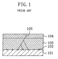
- FIG. 1 is a cross-sectional view of a substrate on which a strained Si crystal layer has been formed by a conventional method.
- a SiGe crystal layer 103 having a thickness of several micrometers or more that exceeds a critical thickness is epitaxially grown on a Si substrate 101 by CVD.
- dislocations are generated in the SiGe crystal layer 103 , and thus the SiGe crystal layer 103 is subjected to lattice relieving.
- a Si crystal is deposited on the SiGe crystal layer 103 by CVD, to form a strained Si crystal layer 104.
- a method for fabricating a semiconductor wafer comprising the steps of depositing a crystal layer on a Si substrate, at least part of the crystal layer containing Si, Ge and C; depositing a Si crystal layer on the SiGeC crystal layer; annealing the SiGeC crystal layer and the SiC crystal substrate including the deposited Si crystal layer; and dispersing the SiC crystals in the SiGeC crystal layer.
- a large defect running through the crystal layer (a through dislocation 105 ) is generated during the formation of the relieved buffer layer made of the SiGe crystal layer 103 having a thickness greater than a critical thickness.
- the through dislocation 105 may even enter the strained Si crystal layer 104 , according to the circumstances, and lead to formation of a defect in the strained Si crystal layer 104 .
- Such a defect in the crystal layer may become a factor impeding improvement of the device characteristics.
- An object of the present invention is proposing a structure and formation method of a relieved buffer layer having a reduced density of crystal defects, and thereby fabricating a semiconductor wafer including a strained Si layer and the like used as a substrate of a semiconductor device.
- the inventive method it is possible to fabricate a semiconductor wafer that uses the crystal layer containing Si, Ge, and C as the relieved buffer layer and enables formation of a strained Si crystal layer hardly having dislocations at positions on the relieved buffer layer.
- step (b) by annealing the substrate to precipitate SiC, it is possible to suppress generation of a through dislocation in the crystal layer as the relieved buffer layer. It is also possible to reduce the thickness of the relieved buffer layer compared with the conventional relieved buffer layer requiring to be as thick as about several micrometers. This enables mass-production of the semiconductor wafer on which a strained Si crystal layer can be formed.
- the inventive method also includes the step of: (c).
- the semiconductor device can exhibit improved performance compared with a semiconductor device using a bulk Si crystal as the substrate.
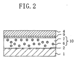
- FIG. 2 is a cross-sectional view of a semiconductor wafer of this embodiment.
- the semiconductor wafer obtained by an method according to of the present invention includes a Si substrate 1 made of a bulk Si crystal, an annealed SiGeC crystal layer 10 having a thickness of about 130 nm formed on the Si substrate 1 , a Si crystal layer 9 having a thickness of about 4 nm formed on the annealed SiGeC crystal layer 10 , and a strained Si crystal layer 4 formed on the Si crystal layer 9 .
- the annealed SiGeC crystal layer 10 includes a matrix SiGeC crystal layer 7 formed on the Si substrate 1 and SiC microcrystals 6 having a diameter of about 2 to 3 nm dispersed in the matrix SiGeC crystal layer 7 .
- Defects 2 suspected of being dislocations are present in a region of the matrix SiGeC crystal layer 7 within 20 nm from the interface with the Si substrate 1 .
- a feature of the wafer of this embodiment is to use the annealed SiGeC crystal layer 10 including the SiC microcrystals 6 and the matrix SiGeC crystal layer 7 as the relieved buffer layer.
- the lattice constant of the lattice-relieved matrix SiGeC crystal layer 7 is greater than the lattice constant of Si. Therefore, although the thickness of the relieved buffer layer is as small as about 130 nm, it is possible to form the strained Si crystal layer 4 by growing the Si crystal layer 9 on the annealed SiGeC crystal layer 10 .
- the crystal defects 2 suspected of being dislocations are confined in the region within 20 nm from the interface between the Si substrate 1 and the annealed SiGeC crystal layer 10 . No through dislocation is observed. The evidence of this, as well as the reasoning by the present inventors on why no through dislocation is generated, will be described later.
- a highly-reliable, high-performance semiconductor device can be fabricated using the semiconductor wafer of this embodiment.
- the thickness of the Si crystal layer 4 is set at 4 nm in this embodiment, it is not specifically limited.
- the Si crystal layer 9 may not necessarily be formed on the annealed SiGeC crystal layer 10, and the strained Si crystal layer 4 may be directly formed on the annealed SiGeC crystal layer 10.
- a SiGe crystal or a SiGeC crystal may be formed under the strained Si crystal layer 4 and on the Si crystal layer 9 .
- the wafer including the strained Si crystal layer 4 was described.
- the wafer may be provided to the user at the stage where the strained Si crystal layer 4 has not been formed.
- composition of the SiGeC crystal in the semiconductor wafer of this embodiment is 68.3% of Si, 30.5% of Ge, and 1.2% of C, as will be described later.
- the contents of these atoms are not limited to these.
- the thickness of the annealed SiGeC crystal layer 10 as the relieved buffer layer is 130 nm.
- a thickness more than 20 nm is enough for the annealed SiGeC crystal layer 10.
- the thickness of the annealed SiGeC crystal layer 10 may exceed 130 nm.
- FIGS. 3A through 3D are cross-sectional views illustrating a fabrication process of the semiconductor wafer of the embodiment of the present invention.
- the surface of the Si substrate 1 in (001) face is cleaned in the following manner.
- the surface of the Si substrate 1 is cleaned with a mixed solution of sulfuric acid - hydrogen peroxide aqueous solution, to remove organic substances and metallic contaminants on the surface of the Si substrate 1.
- the surface of the Si substrate 1 is then cleaned with a solution of ammonia - hydrogen peroxide aqueous solution, to remove attachments on the surface of the Si substrate 1 .
- a naturally-oxidized film on the surface of the Si substrate 1 is removed with hydrofluoric acid.
- the resultant Si substrate 1 is immersed in the solution of ammonia - hydrogen peroxide aqueous solution again, to form a thin protection oxide film on the surface of the Si substrate 1 .
- the surface-cleaned Si substrate 1 is put in an ultrahigh vacuum chemical vapor deposition (UHV-CVD) apparatus, and the inside of the UHV-CVD apparatus is decompressed to as low as 2.6 ⁇ 10 -7 Pa (2 ⁇ 10 -9 Torr).
- UHV-CVD ultrahigh vacuum chemical vapor deposition
- the Si substrate 1 is then heated to a temperature of 800°C in a hydrogen gas atmosphere, to remove the protection oxide film and thus expose the cleaned surface of the Si substrate 1 .
- the temperature of the Si substrate 1 is decreased to 490°C, and while keeping this temperature, disilane (Si 2 H 6 ) gas, germane (GeH 4 ) gas, and methylsilane (SiCH 6 ) gas as material sources of Si, Ge, C, respectively, are introduced into the UHV-CVD apparatus, to permit epitaxial growth of a SiGeC crystal on the Si substrate 1 for 15 minutes, so that the SiGeC crystal layer 8 having a thickness of about 130 nm is deposited.
- disilane (Si 2 H 6 ) gas, germane (GeH 4 ) gas, and methylsilane (SiCH 6 ) gas as material sources of Si, Ge, C, respectively.
- the pressures of the gases during this process are 9.1 ⁇ 10 -3 Pa (7 ⁇ 10 -5 Torr) for the Si 2 H 6 gas, 4.2 ⁇ 10 -2 Pa (3 ⁇ 10 -4 Torr) for the GeH 4 gas, and 1.2 ⁇ 10 -3 Pa (9 ⁇ 10 -6 Torr) for the SiCH 6 gas.
- the feeding of the GeH 4 gas and the SiCH 6 gas is then stopped, and after the substrate temperature is temporarily raised to 550°C, only the Si 2 H 6 gas is fed at a pressure of 3.2 ⁇ 10 -2 Pa (2.4 ⁇ 10 -4 Torr) for 2 minutes, to deposit the Si crystal layer 9 having a thickness of about 4 nm.
- the Si crystal layer 9 serves as a protection film for preventing Ge and C atoms from flowing out to a process apparatus such as a cleaning apparatus used in the next step and contaminating the apparatus.
- the thickness of the Si crystal layer 9 deposited on the SiGeC crystal layer 8 was set at 4 nm. However, it may be thicker or thinner than 4 nm without causing any problem against prevention of contamination. The deposition of the Si crystal layer 9 may even be omitted depending on the structure of the apparatus. Alternatively, a SiGe crystal or a SiGeC crystal may be formed on the Si crystal layer 9 .
- the UHV-CVD method was employed for the crystal growth.
- a LRP apparatus, a RT-CVD apparatus, or the like may be used.
- Si wafer in (001) face was used as the substrate in this embodiment, a Si wafer having a different crystal face may be used.
- FIG. 4 shows XRD spectra of the SiGeC crystal measured immediately after the growth on the Si substrate and after annealing.
- the lower part of FIG. 4 shows the XRD spectrum of the crystal obtained from the substrate immediately after the formation of the SiGeC crystal layer 8 and the Si crystal layer 9 in the step shown in FIG. 3B .
- the peak observed near 34.56 degree is that caused by diffraction from (004) planes of Si used as the substrate, and the peak near 34.06 degree is that caused by the SiGeC crystal deposited on the Si substrate 1 .
- This SiGeC crystal is considered to be in the completely strained state, that is, the state in which any lattice constant of the SiGeC crystal in directions in parallel with the Si substrate completely matches with the lattice constant of the Si substrate.
- the composition of the crystal was estimated from the peak angle of the X-ray diffraction spectrum using a crystal analysis technique called Vegard's Law. As a result, the crystal was found to be a SiGeC crystal containing 30.5% of Ge and about 1.2% of C. Further, from close observation of the lower spectrum in FIG. 4 , it is found that small peaks exist around the peak of the SiGeC crystal near 34.06 degree. These small peaks, which constitute a fringe in the X-ray diffraction image, indicate that the crystallinity and flatness of the SiGeC crystal formed in this embodiment are very good. In order to confirm the crystallinity of the crystal, a cross-sectional view of the crystal was observed by a transmission electron microscope (TEM). And it was found that no defect or the like was observed at all at the interface between the Si substrate 1 and the deposited SiGeC crystal layer 8 and inside the SiGeC crystal layer 8 .
- TEM transmission electron microscope
- the substrate is taken out from the UHV-CVD apparatus, and then annealed in a nitrogen atmosphere with a halogen lamp annealing apparatus, an electric furnace annealing apparatus, or the like.
- the annealing is performed at 1050°C for 15 seconds.
- the SiGeC crystal layer 8 is phase-separated into the SiC microcrystals 6 and the matrix SiGeC crystal layer 7 as will be described later.
- lattice relieving occurs, and as a result, the lattice constant in the plane of the matrix SiGeC crystal layer 7 becomes greater than the lattice constant of the Si substrate 1, as will be described later.
- the substrate was annealed at 1050°C in this embodiment, the annealing may be performed at a temperature at which SiC is precipitated, that is, about 950°C or more.
- the substrate was temporarily taken out of the crystal growth apparatus before starting the annealing. This procedure is not necessarily followed, but the annealing may be sequentially performed in the crystal growth apparatus after the deposition of the SiGeC crystal layer 8.
- FIG. 6 is a TEM micrograph showing the results of observation of a section of the substrate after annealing with a TEM. From FIG. 6 , it is found that the SiC microcrystals 6 having a diameter of about 2 to 3 nm were precipitated in the region that would have otherwise maintained a uniform SiGeC crystal. The SiC microcrystals 6 were presumably generated because the metastable SiGeC crystal was phase-separated by the annealing into the SiC crystals and the SiGe crystal as stable crystals.
- the SiC microcrystals 6 are shown as occupying a greater proportion than the actual volume proportion thereof for easy understanding. In reality, the volume proportion of the SiC microcrystals 6 in the annealed SiGeC crystal layer 10 is considerably small.
- the defects 2 suspected of being dislocations are found only in the region within about 20 nm from the interface between the Si substrate 1 and the annealed SiGeC crystal layer 10 in the matrix SiGeC crystal layer 7 .
- the other region of the matrix SiGeC crystal layer 7 that is, in the region apart from the interface between the Si substrate 1 and the annealed SiGeC crystal layer 10 by more than 20 nm, defects are hardly found. It is known that in general when a structure of a mere SiGe crystal deposited on a Si substrate is annealed, a large through dislocation and the like are generated.
- FIG. 7 is a TEM micrograph taken after annealing of a SiGe crystal formed on a substrate. From FIG. 7 , it is found that a through dislocation was generated in the SiGe layer after annealing. Such a defect was not generated at all in the wafer including the SiGeC layer fabricated in this embodiment.
- the upper spectrum in FIG. 4 shows the results of X-ray diffraction of the substrate after the annealing (see FIG. 3B ).
- the peak appearing at 33.95 degree corresponds to a diffraction peak caused by the SiGeC crystal layer 7. From close analysis using the peak angle and Vegard's Law, it is found that relieving occurred in the matrix SiGeC crystal layer 7 and the interstitial distance in the plane of the matrix SiGeC crystal layer 7 is about 0.5494 nm, which is larger than the lattice constant of Si by about 0.6%.
- this value covers only the matrix SiGeC crystal layer 7 , and is not the lattice constant of the annealed SiGeC crystal layer 10 including the SiC microcrystals. However, since the volume proportion of the SiC microcrystals is considerably small as described above, this value can be regarded equal to the lattice constant of the annealed SiGeC crystal layer 10 .
- the structure of the present invention which includes the Si substrate and the SiGeC crystal layer with SiC crystals dispersed therein, functions as the relieved buffer layer having a reduced defect.
- defects of the crystal structure generated only in the region within 20 nm from the interface between the Si substrate 1 and the annealed SiGeC crystal layer 10 in the matrix SiGeC crystal layer 7 .
- a wafer free from a defect such as a through dislocation can be fabricated by only forming a deposited layer considerably thinner than that formed in this embodiment.
- the surface of the substrate including the Si substrate 1 , the annealed SiGe crystal layer 10 , and the Si crystal layer 9 is cleaned in substantially the same manner as that adopted in the step shown in FIG. 3A .
- the substrate is then put in the UHV-CVD apparatus, and the cleaned substrate surface is exposed inside.
- the substrate temperature is set at 550°C.
- a Si 2 H 6 gas is fed at a pressure of 3.2 ⁇ 10 -2 Pa (2.4 ⁇ 10 -4 Torr) for 15 minutes, to epitaxially grow a Si crystal layer having a thickness of about 30 nm on the Si crystal layer 9 .
- the annealed SiGeC crystal layer 10 and the Si crystal layer 9 are greater in the lattice constant in the plane than the Si substrate 1 . Therefore, the newly deposited Si crystal layer has a lattice constant greater than the Si substrate 1 and therefore constitutes the strained Si crystal layer 4 that has strain.
- a semiconductor substrate including a strained Si crystal layer is fabricated.
- the wafer including the strained Si crystal layer 4 By using the wafer including the strained Si crystal layer 4 , a semiconductor device superior in performance to the conventional semiconductor device using a Si crystal can be fabricated. For example, this makes it possible to fabricate a field effect transistor having a Si/SiGeC heterostructure in which a gate oxide film and a gate electrode are formed on the strained Si crystal layer 4 .
- the thickness of the relieved buffer layer is as small as 130 nm
- the time and cost required for fabrication can be widely reduced compared with the conventional method. This permits mass-production of the semiconductor wafer including the strained Si crystal layer 4.
- FIG. 5 is a view showing the results of measurement of an X-ray diffraction spectrum of the Si substrate 1 with the annealed SiGeC crystal layer 10 and the strained Si crystal layer 4 formed thereon. From FIG. 5 , it is found that, in addition to the diffraction peak of the Si substrate 1 near 34.56 degree and the diffraction peak of the relieved SiGeC crystal (annealed SiGeC crystal layer 10 ) near 33.95 degree, a weak broad peak is observed near 34.7 degree.
- This peak near 34.7 degree is considered to have appeared because the Si crystal layer, which was deposited on the annealed SiGeC crystal layer 10 having a lattice constant in the plane greater than the Si substrate 1 , received tensile stress and thus strained. From analysis using Vegard's Law, it is found that the in-plane lattice constant of the strained Si crystal layer 4 is about 0.5458 nm. Since the interstitial distance of the Si substrate 1 (bulk Si crystal) is 0.5431 nm, the Si crystal layer 4 has a strain of about 0.5%. From the above results, it is found that a strained Si crystal also can be formed by depositing a Si crystal on the SiGeC crystal layer including SiC crystals dispersed therein.
- the present invention is applicable to a field effect transistor that has a Si/SiGeC heterostructure and includes a strained Si crystal, and the like.
Landscapes
- Chemical & Material Sciences (AREA)
- Engineering & Computer Science (AREA)
- Crystallography & Structural Chemistry (AREA)
- Materials Engineering (AREA)
- Metallurgy (AREA)
- Organic Chemistry (AREA)
- Inorganic Chemistry (AREA)
- Recrystallisation Techniques (AREA)
- Insulated Gate Type Field-Effect Transistor (AREA)
- Crystals, And After-Treatments Of Crystals (AREA)
Applications Claiming Priority (3)
| Application Number | Priority Date | Filing Date | Title |
|---|---|---|---|
| JP2000086117 | 2000-03-27 | ||
| JP2000086117A JP4406995B2 (ja) | 2000-03-27 | 2000-03-27 | 半導体基板および半導体基板の製造方法 |
| PCT/JP2001/002523 WO2001073827A1 (en) | 2000-03-27 | 2001-03-27 | Semiconductor wafer and production method therefor |
Publications (3)
| Publication Number | Publication Date |
|---|---|
| EP1197992A1 EP1197992A1 (en) | 2002-04-17 |
| EP1197992A4 EP1197992A4 (en) | 2004-12-29 |
| EP1197992B1 true EP1197992B1 (en) | 2008-08-20 |
Family
ID=18602333
Family Applications (1)
| Application Number | Title | Priority Date | Filing Date |
|---|---|---|---|
| EP01915871A Expired - Lifetime EP1197992B1 (en) | 2000-03-27 | 2001-03-27 | Production method for a semiconductor wafer |
Country Status (8)
| Country | Link |
|---|---|
| US (2) | US6645836B2 (enExample) |
| EP (1) | EP1197992B1 (enExample) |
| JP (1) | JP4406995B2 (enExample) |
| KR (1) | KR20020019037A (enExample) |
| CN (1) | CN1364309A (enExample) |
| DE (1) | DE60135425D1 (enExample) |
| TW (1) | TW495845B (enExample) |
| WO (1) | WO2001073827A1 (enExample) |
Families Citing this family (65)
| Publication number | Priority date | Publication date | Assignee | Title |
|---|---|---|---|---|
| US6744079B2 (en) * | 2002-03-08 | 2004-06-01 | International Business Machines Corporation | Optimized blocking impurity placement for SiGe HBTs |
| WO2002101833A1 (en) * | 2001-06-07 | 2002-12-19 | Amberwave Systems Corporation | Multiple gate insulators with strained semiconductor heterostructures |
| WO2004012243A2 (en) | 2002-07-29 | 2004-02-05 | Amberwave Systems | Selective placement of dislocation arrays |
| GB0220438D0 (en) * | 2002-09-03 | 2002-10-09 | Univ Warwick | Formation of lattice-turning semiconductor substrates |
| CN1286157C (zh) * | 2002-10-10 | 2006-11-22 | 松下电器产业株式会社 | 半导体装置及其制造方法 |
| US6707106B1 (en) * | 2002-10-18 | 2004-03-16 | Advanced Micro Devices, Inc. | Semiconductor device with tensile strain silicon introduced by compressive material in a buried oxide layer |
| US6730576B1 (en) * | 2002-12-31 | 2004-05-04 | Advanced Micro Devices, Inc. | Method of forming a thick strained silicon layer and semiconductor structures incorporating a thick strained silicon layer |
| EP1439570A1 (en) * | 2003-01-14 | 2004-07-21 | Interuniversitair Microelektronica Centrum ( Imec) | SiGe strain relaxed buffer for high mobility devices and a method of fabricating it |
| US6995427B2 (en) | 2003-01-29 | 2006-02-07 | S.O.I.Tec Silicon On Insulator Technologies S.A. | Semiconductor structure for providing strained crystalline layer on insulator and method for fabricating same |
| US7238595B2 (en) * | 2003-03-13 | 2007-07-03 | Asm America, Inc. | Epitaxial semiconductor deposition methods and structures |
| US7682947B2 (en) * | 2003-03-13 | 2010-03-23 | Asm America, Inc. | Epitaxial semiconductor deposition methods and structures |
| US20060225642A1 (en) * | 2003-03-31 | 2006-10-12 | Yoshihiko Kanzawa | Method of forming semiconductor crystal |
| US7517768B2 (en) * | 2003-03-31 | 2009-04-14 | Intel Corporation | Method for fabricating a heterojunction bipolar transistor |
| US6900502B2 (en) * | 2003-04-03 | 2005-05-31 | Taiwan Semiconductor Manufacturing Company, Ltd. | Strained channel on insulator device |
| WO2005013375A1 (ja) * | 2003-08-05 | 2005-02-10 | Fujitsu Limited | 半導体装置及びその製造方法 |
| DE10344986B4 (de) * | 2003-09-27 | 2008-10-23 | Forschungszentrum Dresden - Rossendorf E.V. | Verfahren zur Erzeugung verbesserter heteroepitaktischer gewachsener Siliziumkarbidschichten auf Siliziumsubstraten |
| US7183593B2 (en) * | 2003-12-05 | 2007-02-27 | Taiwan Semiconductor Manufacturing Company, Ltd. | Heterostructure resistor and method of forming the same |
| US7064037B2 (en) * | 2004-01-12 | 2006-06-20 | Chartered Semiconductor Manufacturing Ltd. | Silicon-germanium virtual substrate and method of fabricating the same |
| EP1763893A2 (en) * | 2004-02-27 | 2007-03-21 | ASM America, Inc. | Germanium deposition |
| US20060071213A1 (en) * | 2004-10-04 | 2006-04-06 | Ce Ma | Low temperature selective epitaxial growth of silicon germanium layers |
| KR100708942B1 (ko) * | 2005-12-22 | 2007-04-17 | 매그나칩 반도체 유한회사 | 반도체 웨이퍼 및 그 제조방법 |
| US7560326B2 (en) | 2006-05-05 | 2009-07-14 | International Business Machines Corporation | Silicon/silcion germaninum/silicon body device with embedded carbon dopant |
| US7648853B2 (en) | 2006-07-11 | 2010-01-19 | Asm America, Inc. | Dual channel heterostructure |
| JP4916247B2 (ja) * | 2006-08-08 | 2012-04-11 | トヨタ自動車株式会社 | 炭化珪素半導体装置及びその製造方法 |
| US20080206965A1 (en) * | 2007-02-27 | 2008-08-28 | International Business Machines Corporation | STRAINED SILICON MADE BY PRECIPITATING CARBON FROM Si(1-x-y)GexCy ALLOY |
| US20090108291A1 (en) * | 2007-10-26 | 2009-04-30 | United Microelectronics Corp. | Semiconductor device and method for fabricating the same |
| US8187955B2 (en) | 2009-08-24 | 2012-05-29 | International Business Machines Corporation | Graphene growth on a carbon-containing semiconductor layer |
| US8466502B2 (en) | 2011-03-24 | 2013-06-18 | United Microelectronics Corp. | Metal-gate CMOS device |
| US8445363B2 (en) | 2011-04-21 | 2013-05-21 | United Microelectronics Corp. | Method of fabricating an epitaxial layer |
| US8324059B2 (en) | 2011-04-25 | 2012-12-04 | United Microelectronics Corp. | Method of fabricating a semiconductor structure |
| US8426284B2 (en) | 2011-05-11 | 2013-04-23 | United Microelectronics Corp. | Manufacturing method for semiconductor structure |
| US8481391B2 (en) | 2011-05-18 | 2013-07-09 | United Microelectronics Corp. | Process for manufacturing stress-providing structure and semiconductor device with such stress-providing structure |
| US8431460B2 (en) | 2011-05-27 | 2013-04-30 | United Microelectronics Corp. | Method for fabricating semiconductor device |
| US8716750B2 (en) | 2011-07-25 | 2014-05-06 | United Microelectronics Corp. | Semiconductor device having epitaxial structures |
| US8575043B2 (en) | 2011-07-26 | 2013-11-05 | United Microelectronics Corp. | Semiconductor device and manufacturing method thereof |
| US8647941B2 (en) | 2011-08-17 | 2014-02-11 | United Microelectronics Corp. | Method of forming semiconductor device |
| US8674433B2 (en) | 2011-08-24 | 2014-03-18 | United Microelectronics Corp. | Semiconductor process |
| US8476169B2 (en) | 2011-10-17 | 2013-07-02 | United Microelectronics Corp. | Method of making strained silicon channel semiconductor structure |
| US8691659B2 (en) | 2011-10-26 | 2014-04-08 | United Microelectronics Corp. | Method for forming void-free dielectric layer |
| US8754448B2 (en) | 2011-11-01 | 2014-06-17 | United Microelectronics Corp. | Semiconductor device having epitaxial layer |
| US8647953B2 (en) | 2011-11-17 | 2014-02-11 | United Microelectronics Corp. | Method for fabricating first and second epitaxial cap layers |
| US8709930B2 (en) | 2011-11-25 | 2014-04-29 | United Microelectronics Corp. | Semiconductor process |
| US9127345B2 (en) | 2012-03-06 | 2015-09-08 | Asm America, Inc. | Methods for depositing an epitaxial silicon germanium layer having a germanium to silicon ratio greater than 1:1 using silylgermane and a diluent |
| US9136348B2 (en) | 2012-03-12 | 2015-09-15 | United Microelectronics Corp. | Semiconductor structure and fabrication method thereof |
| US9202914B2 (en) | 2012-03-14 | 2015-12-01 | United Microelectronics Corporation | Semiconductor device and method for fabricating the same |
| US8664069B2 (en) | 2012-04-05 | 2014-03-04 | United Microelectronics Corp. | Semiconductor structure and process thereof |
| US8866230B2 (en) | 2012-04-26 | 2014-10-21 | United Microelectronics Corp. | Semiconductor devices |
| US8835243B2 (en) | 2012-05-04 | 2014-09-16 | United Microelectronics Corp. | Semiconductor process |
| US8951876B2 (en) | 2012-06-20 | 2015-02-10 | United Microelectronics Corp. | Semiconductor device and manufacturing method thereof |
| US8796695B2 (en) | 2012-06-22 | 2014-08-05 | United Microelectronics Corp. | Multi-gate field-effect transistor and process thereof |
| US9171715B2 (en) | 2012-09-05 | 2015-10-27 | Asm Ip Holding B.V. | Atomic layer deposition of GeO2 |
| US8710632B2 (en) | 2012-09-07 | 2014-04-29 | United Microelectronics Corp. | Compound semiconductor epitaxial structure and method for fabricating the same |
| US9117925B2 (en) | 2013-01-31 | 2015-08-25 | United Microelectronics Corp. | Epitaxial process |
| US8753902B1 (en) | 2013-03-13 | 2014-06-17 | United Microelectronics Corp. | Method of controlling etching process for forming epitaxial structure |
| US9034705B2 (en) | 2013-03-26 | 2015-05-19 | United Microelectronics Corp. | Method of forming semiconductor device |
| US9064893B2 (en) | 2013-05-13 | 2015-06-23 | United Microelectronics Corp. | Gradient dopant of strained substrate manufacturing method of semiconductor device |
| US9076652B2 (en) | 2013-05-27 | 2015-07-07 | United Microelectronics Corp. | Semiconductor process for modifying shape of recess |
| US8853060B1 (en) | 2013-05-27 | 2014-10-07 | United Microelectronics Corp. | Epitaxial process |
| US8765546B1 (en) | 2013-06-24 | 2014-07-01 | United Microelectronics Corp. | Method for fabricating fin-shaped field-effect transistor |
| US8895396B1 (en) | 2013-07-11 | 2014-11-25 | United Microelectronics Corp. | Epitaxial Process of forming stress inducing epitaxial layers in source and drain regions of PMOS and NMOS structures |
| US8981487B2 (en) | 2013-07-31 | 2015-03-17 | United Microelectronics Corp. | Fin-shaped field-effect transistor (FinFET) |
| US9224822B2 (en) | 2013-09-10 | 2015-12-29 | Globalfoundries Inc. | High percentage silicon germanium alloy fin formation |
| US9218963B2 (en) | 2013-12-19 | 2015-12-22 | Asm Ip Holding B.V. | Cyclical deposition of germanium |
| TWI620558B (zh) | 2016-12-20 | 2018-04-11 | 富伯生醫科技股份有限公司 | 穿戴式手部復健輔具系統 |
| CN114000120B (zh) | 2022-01-05 | 2022-03-15 | 武汉大学 | 一种基于cvd法的应变金刚石生长掺杂方法 |
Family Cites Families (4)
| Publication number | Priority date | Publication date | Assignee | Title |
|---|---|---|---|---|
| JP2798576B2 (ja) * | 1993-01-27 | 1998-09-17 | 日本電気株式会社 | シリコン膜の成長方法 |
| JPH0722330A (ja) * | 1993-06-29 | 1995-01-24 | Oki Electric Ind Co Ltd | 歪ヘテロエピタキシャル層の形成方法 |
| EP0799495A4 (en) * | 1994-11-10 | 1999-11-03 | Lawrence Semiconductor Researc | Silicon-germanium-carbon compositions and processes thereof |
| JPH11233440A (ja) * | 1998-02-13 | 1999-08-27 | Toshiba Corp | 半導体装置 |
-
2000
- 2000-03-27 JP JP2000086117A patent/JP4406995B2/ja not_active Expired - Fee Related
-
2001
- 2001-03-27 KR KR1020017015163A patent/KR20020019037A/ko not_active Withdrawn
- 2001-03-27 EP EP01915871A patent/EP1197992B1/en not_active Expired - Lifetime
- 2001-03-27 TW TW090107219A patent/TW495845B/zh not_active IP Right Cessation
- 2001-03-27 CN CN01800521A patent/CN1364309A/zh active Pending
- 2001-03-27 WO PCT/JP2001/002523 patent/WO2001073827A1/ja not_active Ceased
- 2001-03-27 DE DE60135425T patent/DE60135425D1/de not_active Expired - Fee Related
- 2001-05-27 US US09/979,305 patent/US6645836B2/en not_active Expired - Lifetime
-
2003
- 2003-04-16 US US10/414,106 patent/US6930026B2/en not_active Expired - Lifetime
Also Published As
| Publication number | Publication date |
|---|---|
| DE60135425D1 (enExample) | 2008-10-02 |
| CN1364309A (zh) | 2002-08-14 |
| US6930026B2 (en) | 2005-08-16 |
| US20020160584A1 (en) | 2002-10-31 |
| US20030203599A1 (en) | 2003-10-30 |
| WO2001073827A1 (en) | 2001-10-04 |
| KR20020019037A (ko) | 2002-03-09 |
| US6645836B2 (en) | 2003-11-11 |
| JP4406995B2 (ja) | 2010-02-03 |
| EP1197992A4 (en) | 2004-12-29 |
| EP1197992A1 (en) | 2002-04-17 |
| TW495845B (en) | 2002-07-21 |
| JP2001274090A (ja) | 2001-10-05 |
Similar Documents
| Publication | Publication Date | Title |
|---|---|---|
| EP1197992B1 (en) | Production method for a semiconductor wafer | |
| US6787793B2 (en) | Strained Si device with first SiGe layer with higher Ge concentration being relaxed to have substantially same lattice constant as second SiGe layer with lower Ge concentration | |
| US7405142B2 (en) | Semiconductor substrate and field-effect transistor, and manufacturing method for same | |
| US7357838B2 (en) | Relaxed silicon germanium substrate with low defect density | |
| US7198997B2 (en) | Method for producing semiconductor substrate, method for producing field effect transistor, semiconductor substrate, and field effect transistor | |
| EP1437765B1 (en) | Production method for semiconductor substrate and production method for field effect transistor | |
| US7138650B2 (en) | Semiconductor substrate, field-effect transistor, and their manufacturing method of the same | |
| US20100019278A1 (en) | Multilayer Structure Comprising A Substrate and A Layer Of Silicon and Germanium Deposited Heteroepitaxially Thereon, and A Process For Producing It | |
| KR20200074898A (ko) | 단결정 구조를 제조하기 위한 방법 | |
| EP1197997A1 (en) | Method for producing semiconductor crystal | |
| JP4700324B2 (ja) | 半導体基板の製造方法 | |
| US20120112190A1 (en) | Epitaxial silicon wafer and method for manufacturing same | |
| JP7347350B2 (ja) | エピタキシャル成長条件の設定方法及びエピタキシャルウェーハの製造方法 | |
| JP4158607B2 (ja) | 半導体基板の製造方法 | |
| JP4120163B2 (ja) | Siエピタキシャルウェーハの製造方法及びSiエピタキシャルウェーハ | |
| US7202142B2 (en) | Method for producing low defect density strained -Si channel MOSFETS | |
| WO2023100540A1 (ja) | 窒化物半導体基板及びその製造方法 | |
| JP2004349522A (ja) | 半導体基板の製造方法 | |
| CN120936082A (zh) | 半导体结构制备方法及半导体结构 | |
| WO2025009407A1 (ja) | ヘテロエピタキシャルウェーハおよびその製造方法 | |
| US7790566B2 (en) | Semiconductor surface treatment for epitaxial growth | |
| JP2009272504A (ja) | 多層膜構造体およびその形成方法 |
Legal Events
| Date | Code | Title | Description |
|---|---|---|---|
| PUAI | Public reference made under article 153(3) epc to a published international application that has entered the european phase |
Free format text: ORIGINAL CODE: 0009012 |
|
| 17P | Request for examination filed |
Effective date: 20011123 |
|
| AK | Designated contracting states |
Kind code of ref document: A1 Designated state(s): AT BE CH CY DE DK ES FI FR GB GR IE IT LI LU MC NL PT SE TR |
|
| RBV | Designated contracting states (corrected) |
Designated state(s): DE FR GB |
|
| A4 | Supplementary search report drawn up and despatched |
Effective date: 20041117 |
|
| RIC1 | Information provided on ipc code assigned before grant |
Ipc: 7H 01L 21/20 A Ipc: 7H 01L 29/24 B Ipc: 7C 30B 33/00 B Ipc: 7H 01L 29/165 B |
|
| 17Q | First examination report despatched |
Effective date: 20050609 |
|
| 17Q | First examination report despatched |
Effective date: 20050609 |
|
| GRAP | Despatch of communication of intention to grant a patent |
Free format text: ORIGINAL CODE: EPIDOSNIGR1 |
|
| RTI1 | Title (correction) |
Free format text: PRODUCTION METHOD FOR A SEMICONDUCTOR WAFER |
|
| GRAS | Grant fee paid |
Free format text: ORIGINAL CODE: EPIDOSNIGR3 |
|
| GRAA | (expected) grant |
Free format text: ORIGINAL CODE: 0009210 |
|
| AK | Designated contracting states |
Kind code of ref document: B1 Designated state(s): DE FR GB |
|
| REG | Reference to a national code |
Ref country code: GB Ref legal event code: FG4D |
|
| REF | Corresponds to: |
Ref document number: 60135425 Country of ref document: DE Date of ref document: 20081002 Kind code of ref document: P |
|
| RAP2 | Party data changed (patent owner data changed or rights of a patent transferred) |
Owner name: PANASONIC CORPORATION |
|
| PLBE | No opposition filed within time limit |
Free format text: ORIGINAL CODE: 0009261 |
|
| STAA | Information on the status of an ep patent application or granted ep patent |
Free format text: STATUS: NO OPPOSITION FILED WITHIN TIME LIMIT |
|
| 26N | No opposition filed |
Effective date: 20090525 |
|
| PGFP | Annual fee paid to national office [announced via postgrant information from national office to epo] |
Ref country code: DE Payment date: 20090429 Year of fee payment: 9 |
|
| GBPC | Gb: european patent ceased through non-payment of renewal fee |
Effective date: 20090327 |
|
| REG | Reference to a national code |
Ref country code: FR Ref legal event code: ST Effective date: 20091130 |
|
| PG25 | Lapsed in a contracting state [announced via postgrant information from national office to epo] |
Ref country code: FR Free format text: LAPSE BECAUSE OF NON-PAYMENT OF DUE FEES Effective date: 20091123 Ref country code: GB Free format text: LAPSE BECAUSE OF NON-PAYMENT OF DUE FEES Effective date: 20090327 |
|
| PG25 | Lapsed in a contracting state [announced via postgrant information from national office to epo] |
Ref country code: DE Free format text: LAPSE BECAUSE OF NON-PAYMENT OF DUE FEES Effective date: 20101001 |