EP1184891B1 - Electron beam lithography - Google Patents
Electron beam lithography Download PDFInfo
- Publication number
- EP1184891B1 EP1184891B1 EP00307641A EP00307641A EP1184891B1 EP 1184891 B1 EP1184891 B1 EP 1184891B1 EP 00307641 A EP00307641 A EP 00307641A EP 00307641 A EP00307641 A EP 00307641A EP 1184891 B1 EP1184891 B1 EP 1184891B1
- Authority
- EP
- European Patent Office
- Prior art keywords
- aberrations
- plane
- electron
- projection column
- spherical
- Prior art date
- Legal status (The legal status is an assumption and is not a legal conclusion. Google has not performed a legal analysis and makes no representation as to the accuracy of the status listed.)
- Expired - Lifetime
Links
Images


Classifications
-
- H—ELECTRICITY
- H01—ELECTRIC ELEMENTS
- H01L—SEMICONDUCTOR DEVICES NOT COVERED BY CLASS H10
- H01L21/00—Processes or apparatus adapted for the manufacture or treatment of semiconductor or solid state devices or of parts thereof
- H01L21/02—Manufacture or treatment of semiconductor devices or of parts thereof
- H01L21/027—Making masks on semiconductor bodies for further photolithographic processing not provided for in group H01L21/18 or H01L21/34
-
- H—ELECTRICITY
- H01—ELECTRIC ELEMENTS
- H01J—ELECTRIC DISCHARGE TUBES OR DISCHARGE LAMPS
- H01J37/00—Discharge tubes with provision for introducing objects or material to be exposed to the discharge, e.g. for the purpose of examination or processing thereof
- H01J37/30—Electron-beam or ion-beam tubes for localised treatment of objects
- H01J37/317—Electron-beam or ion-beam tubes for localised treatment of objects for changing properties of the objects or for applying thin layers thereon, e.g. for ion implantation
- H01J37/3174—Particle-beam lithography, e.g. electron beam lithography
-
- B—PERFORMING OPERATIONS; TRANSPORTING
- B82—NANOTECHNOLOGY
- B82Y—SPECIFIC USES OR APPLICATIONS OF NANOSTRUCTURES; MEASUREMENT OR ANALYSIS OF NANOSTRUCTURES; MANUFACTURE OR TREATMENT OF NANOSTRUCTURES
- B82Y10/00—Nanotechnology for information processing, storage or transmission, e.g. quantum computing or single electron logic
-
- B—PERFORMING OPERATIONS; TRANSPORTING
- B82—NANOTECHNOLOGY
- B82Y—SPECIFIC USES OR APPLICATIONS OF NANOSTRUCTURES; MEASUREMENT OR ANALYSIS OF NANOSTRUCTURES; MANUFACTURE OR TREATMENT OF NANOSTRUCTURES
- B82Y40/00—Manufacture or treatment of nanostructures
-
- H—ELECTRICITY
- H01—ELECTRIC ELEMENTS
- H01J—ELECTRIC DISCHARGE TUBES OR DISCHARGE LAMPS
- H01J2237/00—Discharge tubes exposing object to beam, e.g. for analysis treatment, etching, imaging
- H01J2237/153—Correcting image defects, e.g. stigmators
- H01J2237/1534—Aberrations
-
- Y—GENERAL TAGGING OF NEW TECHNOLOGICAL DEVELOPMENTS; GENERAL TAGGING OF CROSS-SECTIONAL TECHNOLOGIES SPANNING OVER SEVERAL SECTIONS OF THE IPC; TECHNICAL SUBJECTS COVERED BY FORMER USPC CROSS-REFERENCE ART COLLECTIONS [XRACs] AND DIGESTS
- Y10—TECHNICAL SUBJECTS COVERED BY FORMER USPC
- Y10S—TECHNICAL SUBJECTS COVERED BY FORMER USPC CROSS-REFERENCE ART COLLECTIONS [XRACs] AND DIGESTS
- Y10S430/00—Radiation imagery chemistry: process, composition, or product thereof
- Y10S430/143—Electron beam
Definitions
- the invention is generally directed to electron patterning, and more particularly electron patterning using scatter-nonscatter masking and even more particularly electron patterning in accordance with the SCALPEL process described in U.S. Patent No. 5,079,112, issued Jan. 7, 1992 .
- the present invention is also applicable to ion patterning.
- An exemplary conventional apparatus 40 depicted in Figure 1 includes an electron or other energy source 41, condenser lens system 42, mask 43 including blocking regions 44 and transparent regions 45, objective lens 46, back focal plane filter 47 shown as provided with on-axis aperture 48, projector lens system 49, exposure medium 50, between lens 51 and stage 52, which together constitute registration and alignment system 53.
- the apparatus 40 is completed by vacuum chamber 54 and air lock 55, the latter providing the specimen exchange.
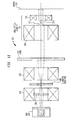
- FIG. 2 Another conventional apparatus shown in Figure 2 includes a particle source 30, illustrated as an electron gun, delivering electron beam 31.
- Collimator lens 32 brings the initially diverging rays into parallel relationship at 33 as shown.
- Scan deflectors 34 and 35 are responsible for electronic scanning, e.g. with continuous x-direction scanning.
- the second deflector provides for y-direction movement, either continuous or as stepped intermediate x-direction scans.
- Mask 36 as depicted again in exemplary terms, is shown as segmented by struts 37.
- the now pattern-containing beam 38 comes under the influence of dynamic focus and stigmator deflectors 39 and 40.
- Deflectors 41 and 42 provide for a precision in placement of adjoining regions during x-and y-electronic scanning/stepping.
- Projection lens 43 is provided with variable axis deflector 44.
- the multiple aperture filter 45 including apertures 46 produces a focused image on wafer 47 shown atop wafer stage 48.
- mask 36 is shown as constituted of pattern regions corresponding with strut-separated segments. Following modulation which imparts patterning information on the beam during passage through mask 36, the beam is converged, finally reaching a crossover (or image inversion) on or near the plane defined by aperture filter 46.
- the aperture filter 45 is included for electron imaging for blocking unwanted scattered radiation. It may serve, as well, to block other "noise" - e.g. by blocking unwanted feature-edge scattered radiation.
- Aperture 46 may define the numerical aperture (or pupil) of the system.
- the apparatus of Figure 1 has separate condenser and projector lens systems. This may be preferred to facilitate focusing with minimum mechanical adjustment. There may be a further preference for multiple lenses in the projector system. For example, use of three lenses is useful to allow correction for image distortion and other aberrations, and to control image rotation as well.
- the exemplary, conventional projector lenses 49, 43 may include other elements, e.g. may include a doublet of two optically equivalent lenses, in operation oppositely polarized to inherently cancel corresponding aberrations implicit to design or operation common to the two. Consistent with usual practice, the hardware responsible for generation of the functional shaped field is, itself, referred to as the "lens".
- lenses 39 and 40 perform dynamic correction for aberration as well as for focusing, e.g. correcting for wafer height variation as well as field curvature. Assigning responsibility for dynamic adjustment to these lenses speeds the process by lessening inductive lag time. For example, dynamic aberration correction may entail additional deflectors compensating for errors resulting from equipment/process defects. Lenses 39 and 40 are illustrative and they may include additional elements.
- Figures 3 and 4 illustrate systems with exemplary optics. Figures 3 and 4 discussed below illustrate schematics serving as a basis for discussing the fundamental principles involved in conventional electron patterning.
- the conventional single lens system depicted in Figure 3 makes use of beam electrons, or other delineating energy, identified as rays 1 incident on mask 2 which includes blocking regions 3 and transparent regions 4. Rays transmitted through transparent regions 4, are identified as rays 1a while those transmitted by blocking regions 3 are identified as rays 1b. Such rays are refracted by lens 5 with emerging rays made incident on back focal plane filter 6. As schematically depicted rays 1a pass through filter aperture 7 to result in image 9 including replicated illuminated regions 10 and unilluminated regions 11. Rays 1b scattered beyond a critical scattering angle, do not pass through aperture 7, but instead are absorbed or otherwise blocked by the non-apertured portion 8 of filter 6.
- FIG. 4 A conventional system in which scattered energy is selectively used to form the image is illustrated in Figure 4 , Here, scattered rays 1b pass through apertures 17 while transmitted rays 1a are now stopped by filter region 18. Image 19 a negative of image 9, results from selective illumination of regions 21. Regions 20 are unilluminated. In this arrangement, the back focal plane filter is absorbing although alternative designs may make use of forms of scattering such as Bragg scattering, etc.
- the projection system(s) illustrated in Figures 1-4 perform mask-to-wafer demagnification, on the order of 4:1-5:1. They are equally applicable to 1:1 and other magnification ratios.
- systems illustrated in Figures 1-4 are arranged so that the resulting image on the wafer is focused as well as possible.
- the goal is to focus the image 60 at the mask 62 on the wafer 64.
- the best focused image 70 occurs at the Gaussian plane 72.
- the best focused image plane 74 usually does not coincide with the Gaussian plane 72.
- Conventional techniques for determining the best focused image plane 74 have concentrated on separately analyzing the effect of chromatic and spherical aberrations on the location of the best focused image plane. These techniques are discussed below.
- a conventional technique for estimating beam focus quality is a point spread function (PSF).
- PSF point spread function
- Typical initial launch conditions included electrons' angular distribution resulting in landing angles up to 12 mrad (up to 10 mrad, or up to 8 mrad), and electrons' actual energy distribution. The latter have been obtained experimentally by analyzing electrons' energy spread before and after passing through a mask 62 (silicon nitride Si x N y , 0.1 ⁇ m thick). An exemplary electron energy distribution is shown in Figure 6 .
- electron passage through the mask 62 introduces an energy spread change: a substantial fraction (up to 20%) of electrons lose energy due to electron-plasmon inelastic collisions.
- Peak A in Figure 6 describes electrons passed through the membrane without losing energy, and its width is defined by the beam source temperature.
- Peak B in Figure 6 describes electrons passed through the membrane with substantial energy losses due to inelastic collisions with the plasmons.
- the energy distribution shown in Figure 6 are characteristic of electron patterning masks, where membrane thickness is smaller than electron mean free path, such as SCALPEL TM mask structures.
- the data shown in Figure 6 can be processed by simulation software developed to compute electron trajectories from the launch point through a projection column (in Figure 5 , the projection doublet 66, 68) down to the wafer 64 plane. Due to 3 rd and 5 th order geometrical aberrations of the lenses in Figure 5 , the image in the Gaussian plane 72 is no longer a point. Analysis has shown that chromatic and spherical aberrations are the most significant aberrations (axial object - axial image). These aberrations create trajectories spread around a central point representing the Gaussian image, and PSF analysis can be used to estimate focus quality as "rise distance", or steepness, of the trajectories' distribution about axis. It has been shown that PSF rise distance defines beam blur, or minimum resolvable feature size at the wafer 64.
- chromatic aberration transforms a point object into a two-dimensional image.
- magnetic and electrostatic lenses alike will focus larger angle electrons closer to the lens plane than small angle ones, thus creating circle of confusion at the ideal, or Gaussian image plane.
- spherical aberration also transforms a point object into a two-dimensional image.
- PSF analysis computes actual electrons' distribution - blur - at any given plane to estimate how close this distribution comes to the ideal, point-like Gaussian image.
- PSF analysis may be used to find the plane in the image space where a circle of confusion reaches its minimum; the search criteria may be chosen as a radial distance between the boundaries drawn in such a manner that one of them represents 12% of total number of electrons launched, and another represents 88% of total number of electrons launched (12/88 criteria). The same procedure can be repeated for boundaries corresponding to 20% and 80% of total number of electrons launched (20/80 criteria). Conventional modeling results for 12/88, taking into account spherical aberration only, are shown in Figure 7 .
- US 6027841 discloses a method for reducing aberrations in charged-particle beam projection exposure.
- the present invention is directed to a method of focusing, wherein spherical aberrations are combined with chromatic aberrations, in order to lessen the negative effect of the chromatic aberrations.
- the present invention is directed to a method of focussing where the spherical aberrations of the projection column reduce a negative defocusing effect caused by chromatic aberrations in the projection column.
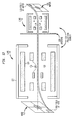
- Figure 11 illustrates an electron patterning system 100.
- the electron patterning system 100 may include a gun 102, a first lens system 104 (with an optical shaping aperture 106 at midplane), a blanking aperture 108, a second lens system 110, a mask 112, a projection doublet 114, including two lenses 116, 118 and a back focal plane 117 (with aperture 117a), and a wafer 120.
- Figure 12 illustrates the mask 112, the projection doublet 114, and a wafer 120 in more detail.
- the lens 116 may include a magnetic shell 122, windings 124, and at least one deflector 126.
- An aperture 128 may be placed between the two lenses 116, 118.
- Figure 12 also illustrates the relationship between the sub-field at the mask 112 and the sub-field at the wafer 120.
- the goal is to place the wafer 120 of Figure 11 in the plane where the image will be best focused.
- conventional techniques for determining the best focus image plane 74 include analyzing and reducing spherical and chromatic aberrations separately.
- the location of the best focus image plane 74 is actually at a location other than where both the spherical and chromatic aberrations separately, are reduced.
- Figure 13 shows the combined effect of the spherical and chromatic aberrations.
- the best focus plane 74 is in fact not located 4 microns in front of the Gaussian plane 72. This is due to the interaction between the spherical and chromatic aberration, the joint effect of these two aberrations actually placing the best focus plane 74 at a location other than the best focus plane for each of the aberrations individually.
- the wafer should be placed in the front of the Gaussian plane, closer to the projection column or optics than a best focus plane for each of the aberrations individually.
- Figures 15-16 explain the interaction between the spherical and chromatic aberrations identified above.
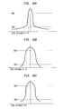
- Figures 15a-15c illustrates the general relationship between PSF and lens aberrations.
- Figure 15a illustrates a PSF at the object plane
- Figure 15b illustrates the PSF at the image plane, with an ideal lens, lens doublet, or projection column, with no aberrations
- Figure 15c illustrates the PSF at the image plane, including an actual lens, lens doublet, or projection column, with aberrations.
- Figure 16a illustrates a PSF broaden by spherical aberration only (using the 20/80 criteria).
- Figure 16b illustrates PSF broadening by chromatic aberration only (also using the 20/80 criteria).
- Figure 16c illustrates the PSF broadening including the joint action of the spherical and chromatic aberrations (also using the 20/80 criteria).
- the addition of the spherical aberration to the chromatic aberration results in a shorter 20/80 rise distance, as a result of PSF curve reshaping.
- the addition of the spherical aberration to the chromatic aberration shapes the PSF in such a way that the slope is steeper in the 20/80 range, which results in an improvement of the lithographic result for the electron beam lithography tool.
- the present invention may be implemented as follows. First an analysis, similar to the analysis performed above in conjunction with Figures 9-10 , is performed to determine the best focus plane, considering chromatic aberrations only. Then the effect of spherical aberrations can be introduced until the best focus plane, considering the combined effect of spherical and chromatic aberrations, is obtained, as illustrated in Figures 13-14 . The wafer is then located at this new best focus plane.
- a spherical aberration coefficient of the projection doublet 116, 118 may be varied by lens design means within a range from 5 mm up to 150 mm. Simulation shows preferred spherical aberration coefficient ranges within 5 to 100 mm. When within this range, spherical aberration helps to decrease beam blur induced by the relatively powerful chromatic aberration.
- Figure 11 describes a gun 102, however, the electron source may be any type of conventional electron source.
- Figure 11 illustrates a first lens system 104, a blanking aperture 108, and a second lens system 110, however, these elements are not necessary.
- Figure 11 illustrates a mask 112
- the mask may be replaced by any similar element, such as a membrane.
- Figure 11 illustrates a projection doublet 114 including lens 116, lens 118 and a back focal plane 117 (with aperture 117a), the projection doublet 114 may be replaced with any number of lenses and other optical elements.
- the goal is to focus the electrons on the wafer 120, the electrons may be focused in any plane on any element, and not necessarily on a wafer.
- the exemplary implementation described above begins with the effect of chromatic aberration only and then considers the effect of spherical aberrations, an alternative implementation could reverse this order.
Landscapes
- Engineering & Computer Science (AREA)
- Chemical & Material Sciences (AREA)
- Nanotechnology (AREA)
- Physics & Mathematics (AREA)
- Crystallography & Structural Chemistry (AREA)
- Condensed Matter Physics & Semiconductors (AREA)
- Manufacturing & Machinery (AREA)
- General Physics & Mathematics (AREA)
- Mathematical Physics (AREA)
- Theoretical Computer Science (AREA)
- Analytical Chemistry (AREA)
- Computer Hardware Design (AREA)
- Microelectronics & Electronic Packaging (AREA)
- Power Engineering (AREA)
- Electron Beam Exposure (AREA)
- Exposure And Positioning Against Photoresist Photosensitive Materials (AREA)
Priority Applications (7)
| Application Number | Priority Date | Filing Date | Title |
|---|---|---|---|
| EP00307641A EP1184891B1 (en) | 2000-09-04 | 2000-09-04 | Electron beam lithography |
| DE60040664T DE60040664D1 (de) | 2000-09-04 | 2000-09-04 | Elektronenstrahl-Lithographie |
| US09/679,403 US6440620B1 (en) | 2000-09-04 | 2000-10-04 | Electron beam lithography focusing through spherical aberration introduction |
| TW90121737A TW574720B (en) | 2000-09-04 | 2001-09-03 | An apparatus and method of focusing |
| JP2001266161A JP4677571B2 (ja) | 2000-09-04 | 2001-09-03 | 電子ビーム投影装置及びフォーカシング方法 |
| KR1020010054187A KR100577754B1 (ko) | 2000-09-04 | 2001-09-04 | 전자빔 리소그라피 장치 및 방법 |
| US10/188,030 US6620565B2 (en) | 2000-09-04 | 2002-07-03 | Electron beam lithography apparatus focused through spherical aberration introduction |
Applications Claiming Priority (1)
| Application Number | Priority Date | Filing Date | Title |
|---|---|---|---|
| EP00307641A EP1184891B1 (en) | 2000-09-04 | 2000-09-04 | Electron beam lithography |
Publications (2)
| Publication Number | Publication Date |
|---|---|
| EP1184891A1 EP1184891A1 (en) | 2002-03-06 |
| EP1184891B1 true EP1184891B1 (en) | 2008-10-29 |
Family
ID=8173243
Family Applications (1)
| Application Number | Title | Priority Date | Filing Date |
|---|---|---|---|
| EP00307641A Expired - Lifetime EP1184891B1 (en) | 2000-09-04 | 2000-09-04 | Electron beam lithography |
Country Status (6)
| Country | Link |
|---|---|
| US (2) | US6440620B1 (ja) |
| EP (1) | EP1184891B1 (ja) |
| JP (1) | JP4677571B2 (ja) |
| KR (1) | KR100577754B1 (ja) |
| DE (1) | DE60040664D1 (ja) |
| TW (1) | TW574720B (ja) |
Families Citing this family (10)
| Publication number | Priority date | Publication date | Assignee | Title |
|---|---|---|---|---|
| US20050048412A1 (en) * | 2003-08-28 | 2005-03-03 | Pary Baluswamy | Methods for reducing spherical aberration effects in photolithography |
| US7489828B2 (en) * | 2003-10-03 | 2009-02-10 | Media Cybernetics, Inc. | Methods, system, and program product for the detection and correction of spherical aberration |
| CN101069260B (zh) * | 2004-08-24 | 2012-09-26 | 西拉半导体工程实验室有限公司 | 工件的离子束铣削及其程度的确定和控制 |
| DE102004048892A1 (de) * | 2004-10-06 | 2006-04-20 | Leica Microsystems Lithography Gmbh | Beleuchtungssystem für eine Korpuskularstrahleinrichtung und Verfahren zur Beleuchtung mit einem Korpuskularstrahl |
| US20060209410A1 (en) * | 2005-03-18 | 2006-09-21 | Smith Adlai H | Method and apparatus for compensation or amelioration of lens field curvature and other imaging defects by utilizing a multi-wavelength setting illumination source |
| EP2228817B1 (en) * | 2009-03-09 | 2012-07-18 | IMS Nanofabrication AG | Global point spreading function in multi-beam patterning |
| US8217352B2 (en) * | 2009-09-11 | 2012-07-10 | Lawrence Livermore National Security, Llc | Ponderomotive phase plate for transmission electron microscopes |
| US8541755B1 (en) * | 2012-05-09 | 2013-09-24 | Jeol Ltd. | Electron microscope |
| US10354206B2 (en) * | 2014-10-02 | 2019-07-16 | Airbnb, Inc. | Determining host preferences for accommodation listings |
| US10248974B2 (en) * | 2016-06-24 | 2019-04-02 | International Business Machines Corporation | Assessing probability of winning an in-flight deal for different price points |
Citations (2)
| Publication number | Priority date | Publication date | Assignee | Title |
|---|---|---|---|---|
| US6027841A (en) * | 1997-12-10 | 2000-02-22 | Nikon Corporation | Charged-particle-beam projection-exposure method exhibiting aberration reduction through multiple deflector use |
| US6069363A (en) * | 1998-02-26 | 2000-05-30 | International Business Machines Corporation | Magnetic-electrostatic symmetric doublet projection lens |
Family Cites Families (7)
| Publication number | Priority date | Publication date | Assignee | Title |
|---|---|---|---|---|
| JPS61240553A (ja) * | 1985-04-18 | 1986-10-25 | Jeol Ltd | イオンビ−ム描画装置 |
| US5079112A (en) * | 1989-08-07 | 1992-01-07 | At&T Bell Laboratories | Device manufacture involving lithographic processing |
| JPH06139983A (ja) * | 1992-10-28 | 1994-05-20 | Nikon Corp | 荷電粒子線装置 |
| JPH0934103A (ja) * | 1995-05-17 | 1997-02-07 | Nikon Corp | 荷電粒子線転写用マスク |
| JPH1070059A (ja) * | 1996-08-26 | 1998-03-10 | Nikon Corp | 荷電粒子線転写装置 |
| JPH1154076A (ja) * | 1997-07-31 | 1999-02-26 | Seiko Instr Inc | 走査型電子顕微鏡用対物レンズ |
| JPH1167642A (ja) * | 1997-08-21 | 1999-03-09 | Nikon Corp | 荷電粒子線投影方法および荷電粒子線投影装置 |
-
2000
- 2000-09-04 DE DE60040664T patent/DE60040664D1/de not_active Expired - Lifetime
- 2000-09-04 EP EP00307641A patent/EP1184891B1/en not_active Expired - Lifetime
- 2000-10-04 US US09/679,403 patent/US6440620B1/en not_active Expired - Lifetime
-
2001
- 2001-09-03 JP JP2001266161A patent/JP4677571B2/ja not_active Expired - Fee Related
- 2001-09-03 TW TW90121737A patent/TW574720B/zh not_active IP Right Cessation
- 2001-09-04 KR KR1020010054187A patent/KR100577754B1/ko active IP Right Grant
-
2002
- 2002-07-03 US US10/188,030 patent/US6620565B2/en not_active Expired - Lifetime
Patent Citations (2)
| Publication number | Priority date | Publication date | Assignee | Title |
|---|---|---|---|---|
| US6027841A (en) * | 1997-12-10 | 2000-02-22 | Nikon Corporation | Charged-particle-beam projection-exposure method exhibiting aberration reduction through multiple deflector use |
| US6069363A (en) * | 1998-02-26 | 2000-05-30 | International Business Machines Corporation | Magnetic-electrostatic symmetric doublet projection lens |
Also Published As
| Publication number | Publication date |
|---|---|
| TW574720B (en) | 2004-02-01 |
| JP2002141281A (ja) | 2002-05-17 |
| KR100577754B1 (ko) | 2006-05-10 |
| US6440620B1 (en) | 2002-08-27 |
| US6620565B2 (en) | 2003-09-16 |
| EP1184891A1 (en) | 2002-03-06 |
| KR20020018981A (ko) | 2002-03-09 |
| JP4677571B2 (ja) | 2011-04-27 |
| US20030022077A1 (en) | 2003-01-30 |
| DE60040664D1 (de) | 2008-12-11 |
Similar Documents
| Publication | Publication Date | Title |
|---|---|---|
| US7408172B2 (en) | Charged particle beam apparatus and charged particle beam irradiation method | |
| US5013913A (en) | Method of illuminating an object in a transmission electron microscope | |
| US20070164228A1 (en) | Aberration correction device and method for operating same | |
| JP2006210503A (ja) | 収差調整方法、デバイス製造方法及び荷電粒子線露光装置 | |
| EP1184891B1 (en) | Electron beam lithography | |
| JP4603305B2 (ja) | 露光方法、パターン寸法調整方法及び焦点ぼかし量取得方法 | |
| US6441384B1 (en) | Charged particle beam exposure device exhibiting reduced image blur | |
| JP2020047589A (ja) | 性能が向上されたマルチ電子ビーム撮像装置 | |
| US6403971B1 (en) | Beam-adjustment methods and apparatus for charged-particle-beam microlithography | |
| JP3678749B2 (ja) | 粒子ビーム、特にイオンの光学像投影システム | |
| US6066853A (en) | Electron-optical system exhibiting reduced aberration | |
| US7521688B2 (en) | Charged-particle beam instrument | |
| JP3280466B2 (ja) | 電子ビーム描画装置 | |
| US6066855A (en) | Charged-particle-beam optical system exhibiting aberration correction | |
| US6563125B1 (en) | Charged-particle-beam microlithography apparatus and methods for preventing coulomb effects using the hollow-beam technique | |
| US6236052B1 (en) | Quadrupole device for projection lithography by means of charged particles | |
| JPH11176720A (ja) | 電子ビーム露光装置 | |
| EP1585165B1 (en) | Electron microscope | |
| JPH1097979A (ja) | 縮小投影装置 | |
| EP1046185B1 (en) | Projection lithography device utilizing charged particles | |
| JPH10303117A (ja) | 電子線光学系 | |
| Abboud et al. | Advanced electron-beam pattern generation technology for 180-nm masks | |
| JP2000306536A (ja) | 拡大結像レンズ系 | |
| JPH1125896A (ja) | 電子光学系 | |
| JPH1027744A (ja) | 荷電粒子線転写装置 |
Legal Events
| Date | Code | Title | Description |
|---|---|---|---|
| PUAI | Public reference made under article 153(3) epc to a published international application that has entered the european phase |
Free format text: ORIGINAL CODE: 0009012 |
|
| AK | Designated contracting states |
Kind code of ref document: A1 Designated state(s): DE FR GB Kind code of ref document: A1 Designated state(s): AT BE CH CY DE DK ES FI FR GB GR IE IT LI LU MC NL PT SE |
|
| AX | Request for extension of the european patent |
Free format text: AL;LT;LV;MK;RO;SI |
|
| 17P | Request for examination filed |
Effective date: 20020906 |
|
| AKX | Designation fees paid |
Free format text: DE FR GB |
|
| 17Q | First examination report despatched |
Effective date: 20071024 |
|
| GRAP | Despatch of communication of intention to grant a patent |
Free format text: ORIGINAL CODE: EPIDOSNIGR1 |
|
| GRAS | Grant fee paid |
Free format text: ORIGINAL CODE: EPIDOSNIGR3 |
|
| GRAA | (expected) grant |
Free format text: ORIGINAL CODE: 0009210 |
|
| AK | Designated contracting states |
Kind code of ref document: B1 Designated state(s): DE FR GB |
|
| REG | Reference to a national code |
Ref country code: GB Ref legal event code: FG4D |
|
| REF | Corresponds to: |
Ref document number: 60040664 Country of ref document: DE Date of ref document: 20081211 Kind code of ref document: P |
|
| RAP4 | Party data changed (patent owner data changed or rights of a patent transferred) |
Owner name: LUCENT TECHNOLOGIES INC. |
|
| PLBE | No opposition filed within time limit |
Free format text: ORIGINAL CODE: 0009261 |
|
| STAA | Information on the status of an ep patent application or granted ep patent |
Free format text: STATUS: NO OPPOSITION FILED WITHIN TIME LIMIT |
|
| 26N | No opposition filed |
Effective date: 20090730 |
|
| REG | Reference to a national code |
Ref country code: FR Ref legal event code: PLFP Year of fee payment: 17 |
|
| REG | Reference to a national code |
Ref country code: DE Ref legal event code: R082 Ref document number: 60040664 Country of ref document: DE Representative=s name: SCHMITT-NILSON SCHRAUD WAIBEL WOHLFROM PATENTA, DE |
|
| REG | Reference to a national code |
Ref country code: FR Ref legal event code: PLFP Year of fee payment: 18 |
|
| PGFP | Annual fee paid to national office [announced via postgrant information from national office to epo] |
Ref country code: DE Payment date: 20170821 Year of fee payment: 18 Ref country code: FR Payment date: 20170822 Year of fee payment: 18 Ref country code: GB Payment date: 20170821 Year of fee payment: 18 |
|
| REG | Reference to a national code |
Ref country code: DE Ref legal event code: R119 Ref document number: 60040664 Country of ref document: DE |
|
| GBPC | Gb: european patent ceased through non-payment of renewal fee |
Effective date: 20180904 |
|
| PG25 | Lapsed in a contracting state [announced via postgrant information from national office to epo] |
Ref country code: DE Free format text: LAPSE BECAUSE OF NON-PAYMENT OF DUE FEES Effective date: 20190402 |
|
| PG25 | Lapsed in a contracting state [announced via postgrant information from national office to epo] |
Ref country code: FR Free format text: LAPSE BECAUSE OF NON-PAYMENT OF DUE FEES Effective date: 20180930 |
|
| PG25 | Lapsed in a contracting state [announced via postgrant information from national office to epo] |
Ref country code: GB Free format text: LAPSE BECAUSE OF NON-PAYMENT OF DUE FEES Effective date: 20180904 |