EP1180794A2 - Prozessführung für eine Metall/Metall-Kontaktherstellung - Google Patents
Prozessführung für eine Metall/Metall-Kontaktherstellung Download PDFInfo
- Publication number
- EP1180794A2 EP1180794A2 EP01117515A EP01117515A EP1180794A2 EP 1180794 A2 EP1180794 A2 EP 1180794A2 EP 01117515 A EP01117515 A EP 01117515A EP 01117515 A EP01117515 A EP 01117515A EP 1180794 A2 EP1180794 A2 EP 1180794A2
- Authority
- EP
- European Patent Office
- Prior art keywords
- etching
- chemical
- metal
- dry etching
- remove
- Prior art date
- Legal status (The legal status is an assumption and is not a legal conclusion. Google has not performed a legal analysis and makes no representation as to the accuracy of the status listed.)
- Ceased
Links
Images




Classifications
-
- H—ELECTRICITY
- H10—SEMICONDUCTOR DEVICES; ELECTRIC SOLID-STATE DEVICES NOT OTHERWISE PROVIDED FOR
- H10P—GENERIC PROCESSES OR APPARATUS FOR THE MANUFACTURE OR TREATMENT OF DEVICES COVERED BY CLASS H10
- H10P70/00—Cleaning of wafers, substrates or parts of devices
- H10P70/20—Cleaning during device manufacture
- H10P70/23—Cleaning during device manufacture during, before or after processing of insulating materials
- H10P70/234—Cleaning during device manufacture during, before or after processing of insulating materials the processing being the formation of vias or contact holes
-
- H—ELECTRICITY
- H10—SEMICONDUCTOR DEVICES; ELECTRIC SOLID-STATE DEVICES NOT OTHERWISE PROVIDED FOR
- H10P—GENERIC PROCESSES OR APPARATUS FOR THE MANUFACTURE OR TREATMENT OF DEVICES COVERED BY CLASS H10
- H10P50/00—Etching of wafers, substrates or parts of devices
- H10P50/20—Dry etching; Plasma etching; Reactive-ion etching
- H10P50/28—Dry etching; Plasma etching; Reactive-ion etching of insulating materials
- H10P50/282—Dry etching; Plasma etching; Reactive-ion etching of insulating materials of inorganic materials
- H10P50/283—Dry etching; Plasma etching; Reactive-ion etching of insulating materials of inorganic materials by chemical means
-
- H—ELECTRICITY
- H10—SEMICONDUCTOR DEVICES; ELECTRIC SOLID-STATE DEVICES NOT OTHERWISE PROVIDED FOR
- H10W—GENERIC PACKAGES, INTERCONNECTIONS, CONNECTORS OR OTHER CONSTRUCTIONAL DETAILS OF DEVICES COVERED BY CLASS H10
- H10W20/00—Interconnections in chips, wafers or substrates
- H10W20/01—Manufacture or treatment
- H10W20/071—Manufacture or treatment of dielectric parts thereof
- H10W20/081—Manufacture or treatment of dielectric parts thereof by forming openings in the dielectric parts
-
- H—ELECTRICITY
- H10—SEMICONDUCTOR DEVICES; ELECTRIC SOLID-STATE DEVICES NOT OTHERWISE PROVIDED FOR
- H10P—GENERIC PROCESSES OR APPARATUS FOR THE MANUFACTURE OR TREATMENT OF DEVICES COVERED BY CLASS H10
- H10P50/00—Etching of wafers, substrates or parts of devices
- H10P50/20—Dry etching; Plasma etching; Reactive-ion etching
- H10P50/28—Dry etching; Plasma etching; Reactive-ion etching of insulating materials
- H10P50/286—Dry etching; Plasma etching; Reactive-ion etching of insulating materials of organic materials
- H10P50/287—Dry etching; Plasma etching; Reactive-ion etching of insulating materials of organic materials by chemical means
Definitions
- the invention relates to a method for producing a Metal / metal contact in the context of a multilayer metallization in an integrated circuit on a semiconductor wafer and an apparatus for performing preprocessing in the case of a metal-to-metal contact production as part of a Multi-layer metallization in an integrated circuit a semiconductor wafer.
- the metal-to-metal contacts are manufactured using conventional methods using planar technology.
- an insulation layer preferably an SiO 2 layer
- a light-sensitive lacquer is then applied, which is then exposed through a mask with the structure of a design level of the contact openings.
- the exposed lacquer is then removed and the SiO 2 layer is anisotropically etched with the aid of plasma etching.
- the remaining photoresist mask is then removed again over the entire area.
- the major part of the photoresists used contains an organic polymer, which can preferably be removed with a plasma etching layer in an oxygen atmosphere.
- a plasma etching layer in an oxygen atmosphere.
- polymer residues are usually deposited in the etched contact hole, which must be removed before metal deposition to fill the contact hole.
- the cleaning process for polymer removal is carried out according to conventional methods as wet chemical etching, in which the semiconductor wafer is immersed in a chemical bath.
- wet film accumulating on the wafer surface during the wet chemical etching leads to undesired oxidation of the metal tracks in the region of the contact opening. Such oxidation is also caused by the fact that when the semiconductor wafer is removed from the chemical bath, it generally comes into contact with air.
- the object of the present invention is the process control for metal / metal contact production in integrated circuits to improve on a semiconductor wafer and in particular to make it cheaper.
- This task is accomplished by a method of manufacturing a Metal / metal contact in the context of a multilayer metallization in an integrated circuit on a semiconductor wafer according to claim 1 and an apparatus for executing the preliminary processes in metal / metal contact production solved according to claim 7. Preferred further developments are in the dependent claims.
- the processes for producing Metal / metal contacts as part of a multi-layer metallization in an integrated circuit on a semiconductor wafer so that after applying an insulation layer a lithography step on a metal level with a photoresist mask to define contact holes the insulation layer and then anisotropic etching the insulation layer for producing the contact holes becomes.
- a vacuum one chemical at a time Dry etching, preferably a plasma etching for removal the photoresist mask, a chemical-physical one Dry etching, preferably reactive ion etching for removal of organic deposits during plasma etching Impurities and a metal deposit for contact hole filling executed.
- plasma etching is used for elimination the photoresist layer and reactive ion etching for removal of organic contaminants that accumulate during plasma etching carried out in a common vacuum chamber, thereby achieving a substantial cost saving that in addition to saving space in the clean room leads.
- an additional disc transport can also be carried out, which involve the risk of oxidation would be waived.
- these two etching techniques can be particularly useful simply in a vacuum chamber using the essentially execute the same equipment.
- etching of the organic contaminants and nitride layer removal be carried out in a common vacuum chamber.
- etching processes namely the removal of the photoresist mask
- the etching of the organic contaminants and nitride layer removal be carried out in a common vacuum chamber.
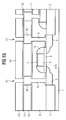
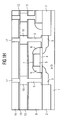
- FIGS. 1A to 1H show a cross section through a silicon wafer in various process stages for training the copper contacts
- Figure 2 shows a comparison of the invention Process sequence with a conventional process sequence
- Figure 4 shows a possible embodiment of an inventive Process chamber.
- FIG. 1A shows a silicon wafer 1 which is weakly p-doped is and in which a field effect transistor is formed.
- This field effect transistor is laterally delimited by two dielectric layers 2, which consist of SiO 2 .
- the field effect transistor has two heavily n-doped diffusion regions 3, which serve as current-supplying (source) and current-receiving (drain) electrodes. Overlapping with these two electrode regions 3, a dielectric layer 4, preferably made of SiO 2 , is formed, on which sits a current-conducting control (gate) electrode 5, which consists, for example, of highly doped polysilicon.
- This gate electrode 5 is delimited by two SiO 2 spacers 6 and connected via a conductor track 7, which preferably consists of tungsten silicide.
- the entire field effect transistor is further encapsulated in an insulation layer 8, which preferably consists of SiO 2 .
- Metal contacts 9, which contact the electrode region 3, are introduced through this insulation layer 8.
- the metal contacts 9 are filled with copper and each connected to a copper conductor 10.
- These copper conductor tracks 10 are enclosed between two nitride layers 11, 12, which provide for an encapsulation of the copper, and for electrical insulation are surrounded by a dielectric layer 13, preferably made of SiO 2 .
- a cross section through the silicon wafer after this manufacturing stage is shown in FIG. 1A.
- a further SiO 2 layer 14 is applied to the upper nitride layer 12 for the electrical insulation of the first conductor track level 10.
- a cross section through the silicon wafer after the SiO 2 deposition is shown in FIG. 1B.
- the structure of the conductor track contacts are defined. This first becomes an adhesion promoter applied to the nitride layer 12 and then the nitride layer 12 coated with a radiation-sensitive photoresist 15.
- This photoresist 15 is generally a so-called Positive photoresist and consists of a solid matrix material, a photosensitive portion and a solvent. The matrix material is primarily a phenolic resin.
- the contact holes are now etched into the SiO 2 layer 14 in a process sequence, the photoresist layer 15 serving as a mask, then the photoresist mask removed again and then the nitride layer 12 etched off on the contact hole bottom.
- All process operations are preferably carried out using dry etching technology, the material being removed by atoms or molecules from a gas and / or by bombarding the surface to be etched with ions, photons or electrons.
- the entire process sequence is carried out in a single process chamber, which is part of a metal separation system, which enables integrated process control without interrupting the vacuum.
- a process chamber according to the invention is shown in FIG. 4.
- This process chamber is preferably connected directly to a system for metal deposition in order to be able to transport the semiconductor wafer from the process chamber into the metal deposition system without interrupting the vacuum.
- the process chamber comprises a closed container 100, a pair of electrodes 110, 111, which is connected to a high-frequency generator 120, an inlet 130 for the etching gas and a connection 140 for the vacuum pump.
- the lower electrode 111 of the electrodes which are preferably arranged in parallel, simultaneously serves as a carrier for the semiconductor wafer 1 to be etched.
- the process chamber shown can be used for chemical dry etching, in which a chemical reaction takes place between neutral particles of a gas and atoms of the surface to be etched, and also a chemical-physical dry etching, in which the chemical etching reaction is supported by a physical etching process which is caused by the bombardment with ions, electrons or photons.
- the chemical-physical etching process is preferably used for the anisotropic etching of the contact holes in the SiO 2 layer and the subsequent cleaning of the contact holes from organic impurities, the chemical etching process, on the other hand, for the surface etching of the photoresist layer.
- the reactor chamber is evacuated and then a suitable one Etching gas supplied.
- a chemical etching process is used performed with an excited gas, the gas in the feed tube by applying a high frequency voltage (not shown) is converted into a plasma.
- This plasma is fed into chamber 100 via inlet 130.
- Out excited neutral diffuse into the plasma Atoms or molecules to the semiconductor wafer 1 and react chemically with the atoms on the surface of the disc.
- the reaction processes are then transferred using a vacuum pump aspirated the connection 140.
- chemical dry etching the etching process is directional, making an isotropic Etching profile is created.
- the etching gas fed via the feed 130 and then by applying one High frequency voltage via the high frequency generator 120 generates a glow discharge on the two electrodes 110, 111, using a low pressure and low temperature plasma Ions, electrons and excited neutral particles are created. Since the electrons in the high-frequency field adapt to the If electrodes attach, these electrodes become negative charged and pull the positive ones out of the plasma Ions. These vertically incident ions then dissolve a chemical etching reaction from the wafer surface, wherein an anisotropic etching profile is created. The etching products are again sucked off from the vacuum pump via connection 140.
- the chemical-physical Dry etching using the reactive ion etching technique where the high frequency voltage is capacitive at the bottom Electrode 111 is applied.
- the upper electrode 110 is connected to the reaction chamber 100 and grounded. Together with the reaction chamber 100 forms the upper electrode 110 such a larger surface than the lower one, which results in has that the lower electrode is more negative from the impinging Electrons being charged.
- the ions from the Plasma thus get on the way to the caustic semiconductor wafer a sufficiently high chemical energy to dissolve chemical etching reactions.
- the gas pressure in the reaction chamber can be kept relatively low, so that the ions hardly collide and are therefore essentially vertical reach the caustic surface and thus the mask true to size on the underlying layer on the semiconductor wafer transfer.
- the silicon wafer After it has been introduced into the reactor chamber 100, is anisotropically etched using a first reactive ion etching step, the photoresist layer 15 serving as the etching mask , SiO 2 is usually etched with a fluorine-containing gas that is selective to the underlying nitride layer 12.
- additives such as H 2 , O 2 , CH 4 etc. are added to the fluorine-containing etching gas for improved etching.
- FIG. 1D The silicon wafer after this etching step is shown in FIG. 1D. However, undesired polymer deposits 16 remain in the contact holes 16 and form from the reaction products of the etching process.
- a dry chemical etching process is carried out which ensures an isotropic etching of the photoresist layer 15.
- Oxygen if appropriate, is preferably used as the etching gas with additives. Even with this isotropic etching process in turn, polymer coatings 16 arise in the contact hole openings 17, like the cross section through the silicon wafer in Figure 1E.
- These polymer deposits 16 are removed in a further reactive ion etching step.
- oxygen is again preferably used as the etching gas, a noble gas, in particular argon, being generally added to stabilize the plasma.
- the remaining SiO 2 layer 14 serves as the etching mask.
- FIG. 1F A cross section through the silicon wafer 1 after this further reactive ion etching process is shown in FIG. 1F.
- Figure 2 shows a comparison of the conventional standard process sequence and the integrated process sequence according to the invention with a copper metallization.
- the standard process sequence are all etching steps in separate etching chambers performed and an argon sputter cleaning before the copper deposition the preheated disc for ablation oxide layers forming in the contact hole openings performed.
- an argon sputter cleaning before the copper deposition the preheated disc for ablation oxide layers forming in the contact hole openings performed.
- the heating step and the subsequent one Sputter cleaning with argon can be integrated in the inventive Process sequence can be dispensed with.
- FIG. 3 shows a further comparison of a conventional one Process sequence and the integrated process sequence according to the invention, where the metallization is done with aluminum becomes. If the conductor tracks are formed with aluminum can be applied to a nitride layer to encapsulate the conductor tracks, as used in copper can be dispensed with. In the conventional methods, however, an additional one wet chemical cleaning after chemical dry etching Photoresist layer made to form polymers remove. This process step is according to the invention replaced by reactive ion etching in the same vacuum system, which has the advantage that there are no oxide layers in the via holes form before the aluminum deposition then again through an additional argon sputtering process must be removed.
Landscapes
- Internal Circuitry In Semiconductor Integrated Circuit Devices (AREA)
- Drying Of Semiconductors (AREA)
Abstract
Description
Claims (6)
- Verfahren zum Herstellen eines Metall/Metall-Kontaktes im Rahmen einer Mehrlagenmetallisierung in einer integrierten Schaltung auf einer Halbleiterscheibe (1) mit den Verfahrensschritten:wobei das chemisches Trockenätzen zur Beseitigung der Fotolackmaske (15), das chemisches-physikalisches Trockenätzen zum Beseitigen von beim Trockenätzen sich anlagernden organischen Verunreinigungen (16) und das Metallabscheiden zum Auffüllen der Kontaktlöcher (17) ohne Unterbrechung des Vakuums durchgeführt wird.Aufbringen einer Isolationsschicht (14) auf einer Metallebene (10),Ausführen eines Fotolithographieschrittes mit einer Fotolackmaske (15) zur Definition von Kontaktlöchern (17) auf der Isolationsschicht (14),anisotropes Ätzen der Isolationsschicht (14) zur Erzeugung der Kontaktlöcher (17),chemisches Trockenätzen zur Beseitigung der Fotolackmaske (15) in einem Vakuum,chemisches-physikalisches Trockenätzen zum Beseitigen von beim Trockenätzen sich anlagernden organischen Verunreinigungen (16) im Vakuum, undMetallabscheiden zum Auffüllen der Kontaktlöcher (17),
- Verfahren nach Anspruch 1, wobei das chemische Trockenätzen zur Beseitigung der Fotolackmaske (15) mit einem Ätzgas durchgeführt wird, das durch Anlegen einer Hochfrequenzspannung oder durch eine Mikrowelleneinkopplung zu einem Plasma angeregt ist.
- Verfahren nach Anspruch 1 oder 2, wobei das chemisch-physikalische Trockenätzen zum Beseitigen der organischen Verunreinigungen (16) mit einer reaktiven Ionenätztechnik durchgeführt wird.
- Verfahren nach einem der Ansprüche 1 bis 3, wobei beim chemischen Trockenätzen zur Beseitigung der Fotolackmaske (15) Sauerstoff als Ätzgas eingesetzt wird.
- Verfahren nach einem der Ansprüche 1 bis 4, wobei zur Metallisierung Kupfer eingesetzt wird und nach dem chemisch-physikalischen Trockenätzen zum Beseitigen organischer Verunreinigungen ein weiterer chemisch-physikalischer Trockenätzschritt im Vakuum zum Entfernen einer Nitrid-Schicht (12) am Kontaktlochboden ausgeführt wird.
- Vorrichtung zum Herstellen eines Metall/Metall-Kontaktes im Rahmen einer Mehrlagenmetallisierung in einer integrierten Schaltung auf einer Halbleiterscheibe (1) gemäß einem der Ansprüche 1 bis 5, umfassend eine Prozesskammer mit einem Behälter (100), der einen Prozessgaseinlass (130), einen Anschluss (140) für eine Vakuumpumpe, Elektroden (110, 111) für eine Hochfrequenzerzeugung und einen Scheibenträger (111) aufweist, wobei der Behälter (100) zum Durchführen nacheinander in einem Vakuum einer chemischen Trockenätzung zum Beseitigen einer Fotolackschicht (15), die als Maske zur Definition von Kontaktlöchern (17) auf einer Isolationsschicht (14), die auf einer Metallebene (10) auf einer Halbleiterscheibe (1) angeordnet ist, dient, und einer chemisch-physikalisches Trockenätzen zum Beseitigen von beim Plasma-Ätzen sich anlagernder organischer Verunreinigungen (16) in den Kontaktlöchern geeignet ist, und wobei die Prozesskammer und die Teil einer Anlage zur Metallabscheidung ist, um einen Transport der Halbleiterscheibe aus der in die Metallabscheideanlage ohne eine Unterbrechung des Vakuums durchführen zu können.
Applications Claiming Priority (2)
| Application Number | Priority Date | Filing Date | Title |
|---|---|---|---|
| DE10040465 | 2000-08-18 | ||
| DE10040465A DE10040465A1 (de) | 2000-08-18 | 2000-08-18 | Prozessführung für eine Metall/Metall-Kontaktherstellung |
Publications (2)
| Publication Number | Publication Date |
|---|---|
| EP1180794A2 true EP1180794A2 (de) | 2002-02-20 |
| EP1180794A3 EP1180794A3 (de) | 2004-08-25 |
Family
ID=7652902
Family Applications (1)
| Application Number | Title | Priority Date | Filing Date |
|---|---|---|---|
| EP01117515A Ceased EP1180794A3 (de) | 2000-08-18 | 2001-07-20 | Prozessführung für eine Metall/Metall-Kontaktherstellung |
Country Status (3)
| Country | Link |
|---|---|
| US (1) | US6596625B2 (de) |
| EP (1) | EP1180794A3 (de) |
| DE (1) | DE10040465A1 (de) |
Families Citing this family (5)
| Publication number | Priority date | Publication date | Assignee | Title |
|---|---|---|---|---|
| RU2436183C1 (ru) * | 2010-08-13 | 2011-12-10 | Федеральное государственное унитарное предприятие "Научно-производственное предприятие "Исток" (ФГУП НПП "Исток") | Способ металлизации элементов изделий электронной техники |
| US8895436B2 (en) | 2012-12-05 | 2014-11-25 | International Business Machines Corporation | Implementing enhanced power supply distribution and decoupling utilizing TSV exclusion zone |
| CN109148287B (zh) * | 2018-08-14 | 2021-01-26 | 苏州芯联成软件有限公司 | 一种高阶芯片反向去层方法 |
| CN111276443B (zh) * | 2020-02-10 | 2023-03-14 | 中国电子科技集团公司第十三研究所 | 微波薄膜混合集成电路的制备方法 |
| CN112435923B (zh) * | 2020-11-27 | 2022-08-16 | 华虹半导体(无锡)有限公司 | 用于多产品混合生产的刻蚀工艺方法 |
Family Cites Families (20)
| Publication number | Priority date | Publication date | Assignee | Title |
|---|---|---|---|---|
| DE4200809C2 (de) * | 1991-03-20 | 1996-12-12 | Samsung Electronics Co Ltd | Verfahren zur Bildung einer metallischen Verdrahtungsschicht in einem Halbleiterbauelement |
| JP3137682B2 (ja) * | 1991-08-12 | 2001-02-26 | 株式会社日立製作所 | 半導体装置の製造方法 |
| KR950009934B1 (ko) * | 1992-09-07 | 1995-09-01 | 삼성전자주식회사 | 반도체 장치의 배선층 형성방법 |
| KR970001883B1 (ko) * | 1992-12-30 | 1997-02-18 | 삼성전자 주식회사 | 반도체장치 및 그 제조방법 |
| US5910021A (en) * | 1994-07-04 | 1999-06-08 | Yamaha Corporation | Manufacture of semiconductor device with fine pattens |
| US5780359A (en) * | 1995-12-11 | 1998-07-14 | Applied Materials, Inc. | Polymer removal from top surfaces and sidewalls of a semiconductor wafer |
| US6013574A (en) * | 1996-01-30 | 2000-01-11 | Advanced Micro Devices, Inc. | Method of forming low resistance contact structures in vias arranged between two levels of interconnect lines |
| US5661083A (en) * | 1996-01-30 | 1997-08-26 | Integrated Device Technology, Inc. | Method for via formation with reduced contact resistance |
| JP2956571B2 (ja) * | 1996-03-07 | 1999-10-04 | 日本電気株式会社 | 半導体装置 |
| US6077768A (en) * | 1996-07-19 | 2000-06-20 | Motorola, Inc. | Process for fabricating a multilevel interconnect |
| JPH1098162A (ja) * | 1996-09-20 | 1998-04-14 | Hitachi Ltd | 半導体集積回路装置の製造方法 |
| CA2193905A1 (en) * | 1996-12-24 | 1998-06-24 | Luc Ouellet | Integrated processing for an etch module |
| US5817579A (en) * | 1997-04-09 | 1998-10-06 | Vanguard International Semiconductor Corporation | Two step plasma etch method for forming self aligned contact |
| JP3667493B2 (ja) * | 1997-05-06 | 2005-07-06 | ヤマハ株式会社 | 半導体装置の製造方法 |
| WO1999006110A1 (en) * | 1997-07-29 | 1999-02-11 | Silicon Genesis Corporation | Cluster tool method and apparatus using plasma immersion ion implantation |
| US6025255A (en) * | 1998-06-25 | 2000-02-15 | Vanguard International Semiconductor Corporation | Two-step etching process for forming self-aligned contacts |
| US6194128B1 (en) * | 1998-09-17 | 2001-02-27 | Taiwan Semiconductor Manufacturing Company | Method of dual damascene etching |
| US6184119B1 (en) * | 1999-03-15 | 2001-02-06 | Vlsi Technology, Inc. | Methods for reducing semiconductor contact resistance |
| US6147007A (en) * | 1999-06-11 | 2000-11-14 | United Microelectronics Corp. | Method for forming a contact hole on a semiconductor wafer |
| US6323121B1 (en) * | 2000-05-12 | 2001-11-27 | Taiwan Semiconductor Manufacturing Company | Fully dry post-via-etch cleaning method for a damascene process |
-
2000
- 2000-08-18 DE DE10040465A patent/DE10040465A1/de not_active Withdrawn
-
2001
- 2001-07-20 EP EP01117515A patent/EP1180794A3/de not_active Ceased
- 2001-08-20 US US09/932,899 patent/US6596625B2/en not_active Expired - Lifetime
Also Published As
| Publication number | Publication date |
|---|---|
| US6596625B2 (en) | 2003-07-22 |
| DE10040465A1 (de) | 2002-03-07 |
| US20020022342A1 (en) | 2002-02-21 |
| EP1180794A3 (de) | 2004-08-25 |
Similar Documents
| Publication | Publication Date | Title |
|---|---|---|
| EP0008359B1 (de) | Verfahren zum Herstellen einer Dünnfilmstruktur | |
| DE60012807T2 (de) | Plasma-Reinigungsverfahren für Öffnungen in Isolierschicht(en) niedriger Dielektrizitätskonstante über Kupferleitungs-IC-Strukturen | |
| DE102006046374B4 (de) | Verfahren zum Reduzieren der Lackvergiftung während des Strukturierens von Siliziumnitridschichten in einem Halbleiterbauelement | |
| DE102009023377B4 (de) | Verfahren zur Herstellung eines Mikrostrukturbauelements mit einer Metallisierungsstruktur mit selbstjustiertem Luftspalt | |
| DE69025300T2 (de) | Integrierte Schaltung mit einer planarisierten dielektrischen Schicht | |
| EP0002669B1 (de) | Verfahren zum Entfernen von Material von einem Substrat durch selektive Trockemätzung und Anwendung dieses Verfahrens bei der Herstellung von Leitungsmustern | |
| DE2720893B2 (de) | ||
| DE102008059650A1 (de) | Mikrostruktur mit einer Metallisierungsstruktur mit selbstjustierten Luftspalten zwischen dichtliegenden Metallleitungen | |
| DE4201661A1 (de) | Verfahren zur herstellung einer halbleiteranordnung | |
| DE2754396A1 (de) | Verfahren zum herstellen von duennfilmmustern | |
| DE68920291T2 (de) | Verfahren zum Herstellen von leitenden Bahnen und Stützen. | |
| DE2709933C2 (de) | Verfahren zur Herstellung von leitenden Verbindungen zwischen übereinander angeordneten Metallisierungsschichten | |
| DE102009023251A1 (de) | Verfahren zur Herstellung eines Kontaktelements mit großem Aspektverhältnis und mit einer günstigeren Form in einem Halbleiterbauelement zur Verbesserung der Abscheidung einer Beschichtung | |
| DE102004017411B4 (de) | In-situ-Metallbarriereablagerung für Sputterätzen auf einer Verbindungsstruktur | |
| DE2734982A1 (de) | Verfahren zum herstellen von silicium enthaltenden leiterzuegen | |
| DE69819023T2 (de) | Methode, eine leitende schicht zu ätzen | |
| DE10340848A1 (de) | Herstellungsverfahren für eine Halbleitereinrichtung | |
| DE102007009913B4 (de) | Plasmaätzprozess mit hoher Ausbeute für Zwischenschichtdielektrika | |
| DE102005052052B4 (de) | Ätzstoppschicht für Metallisierungsschicht mit verbesserter Haftung, Ätzselektivität und Dichtigkeit und Verfahren zur Herstellung eines dielektrischen Schichtstapels | |
| DE102010040071B4 (de) | Verfahren zur Wiederherstellung von Oberflächeneigenschaften empfindlicher Dielektrika mit kleinem ε in Mikrostrukturbauelementen unter Anwendung einer in-situ-Oberflächenmodifizierung | |
| DE102011004581A1 (de) | Technik zur Reduzierung der plasmahervorgerufenen Ätzschäden während der Herstellung von Kontaktdurchführungen in Zwischenschichtdielektrika durch modifizierten HF-Leistungshochlauf | |
| WO2011036089A1 (de) | Verfahren zum herstellen eines elektronischen bauelements sowie elektronisches bauelement | |
| DE10040465A1 (de) | Prozessführung für eine Metall/Metall-Kontaktherstellung | |
| DE10226603A1 (de) | Verfahren zum Strukturieren einer Siliziumschicht sowie dessen Verwendung zur Herstellung einer integrierten Halbleiterschaltung | |
| DE3219284C2 (de) |
Legal Events
| Date | Code | Title | Description |
|---|---|---|---|
| PUAI | Public reference made under article 153(3) epc to a published international application that has entered the european phase |
Free format text: ORIGINAL CODE: 0009012 |
|
| AK | Designated contracting states |
Kind code of ref document: A2 Designated state(s): AT BE CH CY DE DK ES FI FR GB GR IE IT LI LU MC NL PT SE TR |
|
| AX | Request for extension of the european patent |
Free format text: AL;LT;LV;MK;RO;SI |
|
| PUAL | Search report despatched |
Free format text: ORIGINAL CODE: 0009013 |
|
| AK | Designated contracting states |
Kind code of ref document: A3 Designated state(s): AT BE CH CY DE DK ES FI FR GB GR IE IT LI LU MC NL PT SE TR |
|
| AX | Request for extension of the european patent |
Extension state: AL LT LV MK RO SI |
|
| 17P | Request for examination filed |
Effective date: 20040827 |
|
| 17Q | First examination report despatched |
Effective date: 20040928 |
|
| AKX | Designation fees paid |
Designated state(s): DE FR |
|
| RAP1 | Party data changed (applicant data changed or rights of an application transferred) |
Owner name: INFINEON TECHNOLOGIES AG |
|
| RAP1 | Party data changed (applicant data changed or rights of an application transferred) |
Owner name: QIMONDA AG |
|
| STAA | Information on the status of an ep patent application or granted ep patent |
Free format text: STATUS: THE APPLICATION HAS BEEN REFUSED |
|
| 18R | Application refused |
Effective date: 20131207 |