EP1179740A2 - Routage d'une chaine de balayage périphérique - Google Patents
Routage d'une chaine de balayage périphérique Download PDFInfo
- Publication number
- EP1179740A2 EP1179740A2 EP01306739A EP01306739A EP1179740A2 EP 1179740 A2 EP1179740 A2 EP 1179740A2 EP 01306739 A EP01306739 A EP 01306739A EP 01306739 A EP01306739 A EP 01306739A EP 1179740 A2 EP1179740 A2 EP 1179740A2
- Authority
- EP
- European Patent Office
- Prior art keywords
- boundary scan
- control
- scan cells
- control conductor
- signal
- Prior art date
- Legal status (The legal status is an assumption and is not a legal conclusion. Google has not performed a legal analysis and makes no representation as to the accuracy of the status listed.)
- Granted
Links
- 239000004020 conductor Substances 0.000 claims abstract description 97
- 238000012360 testing method Methods 0.000 claims abstract description 26
- 239000004065 semiconductor Substances 0.000 claims abstract description 13
- 238000000034 method Methods 0.000 claims description 10
- 239000000758 substrate Substances 0.000 claims 3
- 230000008878 coupling Effects 0.000 claims 2
- 238000010168 coupling process Methods 0.000 claims 2
- 238000005859 coupling reaction Methods 0.000 claims 2
- 238000010586 diagram Methods 0.000 description 3
- 239000002184 metal Substances 0.000 description 3
- 238000002955 isolation Methods 0.000 description 1
- 238000001465 metallisation Methods 0.000 description 1
- 229910000679 solder Inorganic materials 0.000 description 1
- 230000007704 transition Effects 0.000 description 1
- 230000001960 triggered effect Effects 0.000 description 1
Images


Classifications
-
- G—PHYSICS
- G01—MEASURING; TESTING
- G01R—MEASURING ELECTRIC VARIABLES; MEASURING MAGNETIC VARIABLES
- G01R31/00—Arrangements for testing electric properties; Arrangements for locating electric faults; Arrangements for electrical testing characterised by what is being tested not provided for elsewhere
- G01R31/28—Testing of electronic circuits, e.g. by signal tracer
- G01R31/317—Testing of digital circuits
- G01R31/3181—Functional testing
- G01R31/3185—Reconfiguring for testing, e.g. LSSD, partitioning
- G01R31/318533—Reconfiguring for testing, e.g. LSSD, partitioning using scanning techniques, e.g. LSSD, Boundary Scan, JTAG
- G01R31/318541—Scan latches or cell details
-
- G—PHYSICS
- G01—MEASURING; TESTING
- G01R—MEASURING ELECTRIC VARIABLES; MEASURING MAGNETIC VARIABLES
- G01R31/00—Arrangements for testing electric properties; Arrangements for locating electric faults; Arrangements for electrical testing characterised by what is being tested not provided for elsewhere
- G01R31/28—Testing of electronic circuits, e.g. by signal tracer
- G01R31/317—Testing of digital circuits
- G01R31/3181—Functional testing
- G01R31/3185—Reconfiguring for testing, e.g. LSSD, partitioning
- G01R31/318533—Reconfiguring for testing, e.g. LSSD, partitioning using scanning techniques, e.g. LSSD, Boundary Scan, JTAG
- G01R31/318536—Scan chain arrangements, e.g. connections, test bus, analog signals
- G01R31/318538—Topological or mechanical aspects
-
- G—PHYSICS
- G01—MEASURING; TESTING
- G01R—MEASURING ELECTRIC VARIABLES; MEASURING MAGNETIC VARIABLES
- G01R31/00—Arrangements for testing electric properties; Arrangements for locating electric faults; Arrangements for electrical testing characterised by what is being tested not provided for elsewhere
- G01R31/28—Testing of electronic circuits, e.g. by signal tracer
- G01R31/317—Testing of digital circuits
- G01R31/3181—Functional testing
- G01R31/3185—Reconfiguring for testing, e.g. LSSD, partitioning
- G01R31/318533—Reconfiguring for testing, e.g. LSSD, partitioning using scanning techniques, e.g. LSSD, Boundary Scan, JTAG
- G01R31/318594—Timing aspects
Definitions
- This invention relates to integrated circuits, and more particularly to the routing of boundary scan control conductors to control boundary scan cells associated with the integrated circuit input/output pads.
- boundary scan chains to input data into integrated circuits, test integrated circuits and test systems of integrated circuits has become ubiquitous. IEEE standard 1149.1, and revisions thereto, each of which is hereby incorporated by reference, often referred to as JTAG, defines the logic for implementing a boundary scan chain.
- US patent 5,355,369 discloses a high speed integrated circuit that provides for boundary scan testing, the disclosure of which is hereby incorporated by reference.
- a boundary scan chain is comprised of cells of logic at each input/output path. The input/output paths are typically located around the periphery of an integrated circuit die.
- the logic cells also known as boundary scan cells, are controlled in accordance with the above-mentioned standard by control signals.
- the control signals are typically provided to each boundary scan cell by a "ring" bus proximate the boundary scan cells, with each ring bus conductor being endless, that is forming a loop, and driven at a single point.
- Data is transferred sequentially from one boundary scan cell to an adjacent boundary scan cell.
- data is shifted from any boundary scan cell to an adjacent boundary scan cell in the same manner data is shifted from a register in a shift register to the next register in the shift register.
- a problem that arises with the ring implementation of the control signal conductors is the potential for a race condition.
- the race condition occurs when transferring data between two adjacent latches.
- One of the adjacent latches is the output latch of a boundary scan cell from which data is being transferred and the other of the adjacent latches is the input latch of the adjacent boundary scan cell into which data is being shifted.
- a race condition exists if the skew introduced in the clock control signal between the two adjacent latches is greater than the propagation delay to transfer data from one of the two adjacent latches to the other.
- One technique to overcome the potential race condition is to break the ring bus conductor to which the clock signal is applied.
- the ring bus conductor is broken between the first boundary scan cell and the last boundary scan cell in the boundary scan chain.
- the clock signal drives an end of the broken clock ring bus conductor such that the clock signal propagates around the broken ring in the opposite direction that data is shifted through adjacent boundary scan cells.
- data is shifted around the sequence of boundary scan cells in one direction, for example counter clockwise, while the clock signal propagates around the broken clock ring bus conductor in the opposite direction, for example clockwise, or vice versa.
- Another potential race condition is introduced by breaking the clock ring bus conductor and driving an end of the broken clock ring bus conductor.
- the potential race condition introduced occurs at the first boundary scan cell to receive data.
- the first boundary scan cell receives the clock signal with the greatest skew since the clock signal travels the greatest distance to arrive at the first boundary scan cell.
- the active low shift signal goes low, the data being shifted into the first boundary scan cell passes through the first, master, latch and is latched in a second, slave, latch when the shift signal arrives at the first boundary scan cell before the clock signal arrives (a late clock condition) at the first boundary scan cell.
- an integrated circuit includes a semiconductor die having a plurality of input/output pads.
- a plurality of boundary scan cells one corresponding to each input/output pad, implements boundary scan functions associated with respective input/output pads.
- Each of the boundary scan cells includes a TDI input and a TDO output.
- the boundary scan cells are structured as a shift register to shift data from one boundary scan cell in a direction unilaterally to an adjacent boundary scan cell.
- a first boundary scan cell is the first boundary scan cell of the plurality of boundary scan cells to receive data.
- a last boundary scan cell is the last boundary scan cell of the plurality of boundary scan cells to receive data.
- An endless control conductor forms a loop proximate the plurality of boundary scan cells.
- the endless control conductor is coupled to each of the plurality of boundary scan cells to provide a test clock signal thereto.
- At least one other control conductor extends around the semiconductor die proximate the plurality of boundary scan cells.
- the at least one other control conductor is coupled to each of the plurality of boundary scan cells and is discontinuous between the first and last boundary scan cells.
- the invention may also be implemented at a system level.
- FIG. 1 An enlarged portion of an integrated circuit 10 semiconductor die 12 illustrating routing of boundary scan control conductors in accordance with the invention is illustrated in Figure 1.
- Semiconductor die 12 is not drawn to scale.
- Semiconductor die 12 includes a plurality of bond pads 14 to which bond wires (not shown) are bonded to connect to leads (not shown) or metalizations (not shown) for further interconnection to an array of solder bumps or posts, as is known in the art.
- Bond pads 14 are typically located proximate the periphery of semiconductor die 12. Bond pads 14 provide an interface, to circuits (not shown) on semiconductor die, each of which can provide an input, an output, or both an input and an output, herein referred to as an input/output or input/output port.
- each bond pad 14 Associated with each bond pad 14, except those bond pads representing the JTAG interface 16 and others, is a scan cell or boundary scan cell 18 for testing or programming of the integrated circuit, or testing or programming of a system of integrated circuits.
- Boundary scan cells are comprised of logic circuits and isolation circuitry. Each boundary scan cell 18 can read the logic state of its associated bond pad, drive a logic state onto its associated bond pad, or can be isolated from its associated bond pad 14.
- Boundary scan cells 18 are typically located proximate the associated bond pad 14, and therefore are typically located around the periphery of semiconductor die 12.
- Boundary scan cells 18 are designed to shift data, in the form of one bit, from one boundary scan cell to an adjacent boundary scan cell over lines 20 in a unilateral direction, much like shifting bits into or through registers of a serial shift register In this manner, boundary scan cells 18 form a boundary scan chain 22. As with any serial shift register, until all boundary scan cells have been loaded with meaningful data , the output from the last boundary scan cell in chain 22 is not meaningful.
- Boundary scan cells 18 are controlled by the JTAG test access port (TAP) controller 24. Controller 24 is coupled to each of the bond pads of JTAG interface 16. TCK input pad 26 provides a test clock input. TDI input pad 28 provides test data to the first boundary scan cell in chain 22 to receive data. TRSTN input pad 30 provides a negative triggered reset function. TMS input pad 32 is a test mode select that is provided to controller 24 to select the mode of operation of boundary scan chain 22. When the boundary scan mode is selected, the TDO output pad 34 receives the test data sequenced through the boundary scan cells from the JOUT block 62 over conductor 56.
- TAP JTAG test access port
- a control bus 36 comprised of conductors 38 provide control signals from JTAG interface 16 or controller 24 to each of the boundary scan cells 18.
- Control bus 36 is typically located proximate boundary scan cells 18 and therefore around the periphery of semiconductor die 12.
- Conductors 38 in bus 36 may or may not be continuous or endless, forming a loop proximate the boundary scan cells 18.
- bus 36 is typically fabricated in the top layer of metal. However, the invention is not limited thereto. With appropriate interconnects as is known in the art, bus 36 could be fabricated in more than one layer of metal.
- bus 36 may have more than four conductors. They are clock conductor 40, shift conductor 42, capture conductor 44, and update conductor 46.
- a test clock signal is applied to JTAG interface bond pad 26.
- the test clock signal, TCK is applied to both clock conductor 40 and JTAG block 60.
- JTAG block 60 develops a shift signal which is applied to shift conductor 42, a capture signal which is applied to capture conductor 44, and an update signal which is applied to update conductor 46.
- the shift signal causes data to shift from one boundary scan cell to the next boundary scan cell in chain 22.
- a new data bit is shifted into the first boundary scan cell, first cell 48, in the chain over line 50 from bond pad 28.
- a data bit is shifted out of the last boundary scan cell, last cell 52, in the chain over line 54 to JOUT block62 thence over line 56 to bond pad 34 of JTAG interface 16.
- clock conductor 40 in control bus 36 is endless, or continuos, forming a loop around the boundary scan cells 18 to which it is connected.
- the shift conductor 42, capture conductor 44 and update conductor 46 are interrupted or discontinuous, and are collectively known as interrupted conductors 58.
- Interrupted conductors 58 are driven by controller 24 and the first tap from each of interrupted conductors 58 provides shift, capture and update signals to last cell 52 in chain 22. The second tap from each of conductors 58 provides shift, capture and update signals to the next-to-the-last cell, the boundary scan cell from which last cell 52 receives data.
- the shift, capture and update signals propagate along conductors 42, 44, and 46 respectively to each of the boundary scan cells 18 in chain 22, with first cell 48 being the last boundary scan cell to receive the signals.
- first cell 48 being the last boundary scan cell to receive the signals.
- the shift, capture, and update signals propagate around the boundary scan cells 18 of chain 22 in a direction opposite to the unilateral direction data is shifted from one boundary scan cell 18 to an adjacent boundary scan cell 18 in chain 22.
- the shift, capture and update signals propagate around boundary scan cells 18 of chain 22 in a direction opposite to the unilateral direction data is shifted from one boundary scan cell to an adjacent boundary scan cell due to two factors.
- respective conductors 42, 44, and 46 are interrupted between the tap points where conductors 42, 44, and 46 are connected to last cell 52 and the respective tap points where conductors 42, 44, and 46 are connected to first cell 48.
- the respective signals are impressed on conductors 42, 44, and 46 at the end of the respective conductors proximate the tap point for last cell 52, such that the signals propagate along the conductors from, and are presented to boundary scan cells 18 in chain 22 in a sequence to, last cell 52 to first cell 48.
- FIG. 2 is a schematic diagram of a scan register 80 portion of a typical boundary scan cell 18, including an additional delay line 82.
- Shift, capture and update signals provide control inputs respectively to multiplexers 84, 86, and 88.
- the test data With test data presented at the TDI input of multiplexer 84, the test data is passed to the output of master latch 90 when the shift signal is low and the test clock signal is low, thence to the output of slave latch 92 when the test clock signal transitions high.
- Delay 82 introduces a predetermined delay into presentation of the data at the output of slave latch 92 as the test data output, TDO, of the typical boundary scan cell.
- the duration of the delay is approximately at least 80% of half of the period of the test clock, TCK, signal.
- the delay may be implemented in any known manner.
- the output data from TDO bond pad 34 is provided to a scan module (not shown).
- the scan module operates on the data received to verify that the output data is as expected, and therefore the conclusion may be drawn that the integrated circuit or system that generated the output data is operating correctly.
- Routing the clock, shift, and capture control conductors, and hence the signals imposed thereon, in the manner described above may, in some applications, be sufficient to assure the test clock signal arrives at the first cell 48 before the shift, capture, and update signals arrive at the first cell 48 in a chain 22.
- the shift, capture, and update signals incur a longer propagation delay by the time they reach first cell 48 than the test clock signal incurs by the time it reaches first cell 48 due to the relative lengths of the signal paths the signals take over conductors 38.
- Introducing a predetermined delay to defer the data output from each boundary scan cell obviates the potential race at first cell 48 and assures that the test clock signal will arrive at first cell 48 before the shift, capture, and update signals arrive.
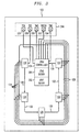
- FIG. 3 illustrates application of the invention to a system.
- Integrated circuits 120 are mounted on circuit board 122. Traces 124 form a bus 126 to interconnect integrated circuits 120 with JTAG control signals and to transfer data. Bus 126 interconnects integrated circuits 120 in a chain 128. Data can be transferred on one trace 124 serially from one integrated circuit to the next integrated circuit in chain 128.
- Each integrated circuit 120 has a boundary scan chain 22 as described above.
- the JTAG control functions for the system may be performed by the JTAG controller and JOUT block of one of the integrated circuits, or there may be, as illustrated in Figure 3, a separate JTAG controller and JOUT block at the system level. From the foregoing description, operation at the system level will be apparent to one skilled in the art.
Landscapes
- Engineering & Computer Science (AREA)
- General Engineering & Computer Science (AREA)
- Physics & Mathematics (AREA)
- General Physics & Mathematics (AREA)
- Tests Of Electronic Circuits (AREA)
- Semiconductor Integrated Circuits (AREA)
Priority Applications (1)
| Application Number | Priority Date | Filing Date | Title |
|---|---|---|---|
| EP05077021A EP1637894B1 (fr) | 2000-08-07 | 2001-08-07 | Routage d'une chaine de balayage périphérique |
Applications Claiming Priority (2)
| Application Number | Priority Date | Filing Date | Title |
|---|---|---|---|
| US633795 | 2000-08-07 | ||
| US09/633,795 US6640324B1 (en) | 2000-08-07 | 2000-08-07 | Boundary scan chain routing |
Related Child Applications (1)
| Application Number | Title | Priority Date | Filing Date |
|---|---|---|---|
| EP05077021A Division EP1637894B1 (fr) | 2000-08-07 | 2001-08-07 | Routage d'une chaine de balayage périphérique |
Publications (3)
| Publication Number | Publication Date |
|---|---|
| EP1179740A2 true EP1179740A2 (fr) | 2002-02-13 |
| EP1179740A3 EP1179740A3 (fr) | 2004-01-07 |
| EP1179740B1 EP1179740B1 (fr) | 2005-10-19 |
Family
ID=24541142
Family Applications (2)
| Application Number | Title | Priority Date | Filing Date |
|---|---|---|---|
| EP01306739A Expired - Lifetime EP1179740B1 (fr) | 2000-08-07 | 2001-08-07 | Routage d'une chaine de balayage périphérique |
| EP05077021A Expired - Lifetime EP1637894B1 (fr) | 2000-08-07 | 2001-08-07 | Routage d'une chaine de balayage périphérique |
Family Applications After (1)
| Application Number | Title | Priority Date | Filing Date |
|---|---|---|---|
| EP05077021A Expired - Lifetime EP1637894B1 (fr) | 2000-08-07 | 2001-08-07 | Routage d'une chaine de balayage périphérique |
Country Status (5)
| Country | Link |
|---|---|
| US (1) | US6640324B1 (fr) |
| EP (2) | EP1179740B1 (fr) |
| JP (1) | JP3876380B2 (fr) |
| DE (2) | DE60136112D1 (fr) |
| TW (1) | TW527629B (fr) |
Cited By (3)
| Publication number | Priority date | Publication date | Assignee | Title |
|---|---|---|---|---|
| EP1221700A1 (fr) * | 2001-11-02 | 2002-07-10 | Siemens Aktiengesellschaft | Module électronique avec mise en oeuvre d'un boundary-scan amélioré |
| WO2005106615A1 (fr) * | 2004-04-29 | 2005-11-10 | International Business Machines Corporation | Procede et appareil de resistance au piratage de materiel par le biais d'une interface de registres internes |
| WO2018151956A1 (fr) * | 2017-02-16 | 2018-08-23 | Qualcomm Incorporated | Configuration d'interface puce-puce et ses procédés d'utilisation |
Families Citing this family (10)
| Publication number | Priority date | Publication date | Assignee | Title |
|---|---|---|---|---|
| US7188277B2 (en) * | 2003-03-28 | 2007-03-06 | Hewlett-Packard Development Company, L.P. | Integrated circuit |
| US7146538B2 (en) * | 2003-03-28 | 2006-12-05 | Hewlett-Packard Development Company, L.P. | Bus interface module |
| US7162673B2 (en) * | 2003-11-14 | 2007-01-09 | Integrated Device Technology, Inc. | Scan chain registers that utilize feedback paths within latch units to support toggling of latch unit outputs during enhanced delay fault testing |
| US7447961B2 (en) * | 2004-07-29 | 2008-11-04 | Marvell International Ltd. | Inversion of scan clock for scan cells |
| KR101681736B1 (ko) | 2010-05-14 | 2016-12-02 | 삼성전자주식회사 | 입출력 래퍼들을 갖는 반도체 장치 |
| US9140754B2 (en) * | 2011-02-28 | 2015-09-22 | Texas Instruments Incorporated | Scan-based MCM interconnecting testing |
| US8793546B2 (en) | 2011-06-20 | 2014-07-29 | Lsi Corporation | Integrated circuit comprising scan test circuitry with parallel reordered scan chains |
| US8671320B2 (en) | 2011-06-21 | 2014-03-11 | Lsi Corporation | Integrated circuit comprising scan test circuitry with controllable number of capture pulses |
| US8615693B2 (en) | 2011-08-31 | 2013-12-24 | Lsi Corporation | Scan test circuitry comprising scan cells with multiple scan inputs |
| CN109298322A (zh) * | 2018-09-27 | 2019-02-01 | 西安微电子技术研究所 | 一种动态变链长扫描结构及其方法和边界扫描单元 |
Citations (2)
| Publication number | Priority date | Publication date | Assignee | Title |
|---|---|---|---|---|
| JPH06289099A (ja) * | 1993-03-30 | 1994-10-18 | Toshiba Corp | スキャン回路 |
| US5488614A (en) * | 1992-03-24 | 1996-01-30 | Nec Corporation | Integrated logic circuit |
Family Cites Families (6)
| Publication number | Priority date | Publication date | Assignee | Title |
|---|---|---|---|---|
| US4063080A (en) * | 1976-06-30 | 1977-12-13 | International Business Machines Corporation | Method of propagation delay testing a level sensitive array logic system |
| US5355369A (en) | 1991-04-26 | 1994-10-11 | At&T Bell Laboratories | High-speed integrated circuit testing with JTAG |
| JP2553292B2 (ja) * | 1991-12-20 | 1996-11-13 | インターナショナル・ビジネス・マシーンズ・コーポレイション | 論理回路テスト装置及び方法 |
| US5701335A (en) * | 1996-05-31 | 1997-12-23 | Hewlett-Packard Co. | Frequency independent scan chain |
| US5898776A (en) * | 1996-11-21 | 1999-04-27 | Quicklogic Corporation | Security antifuse that prevents readout of some but not other information from a programmed field programmable gate array |
| US5991908A (en) * | 1997-09-29 | 1999-11-23 | Xilinx, Inc. | Boundary scan chain with dedicated programmable routing |
-
2000
- 2000-08-07 US US09/633,795 patent/US6640324B1/en not_active Expired - Fee Related
-
2001
- 2001-08-06 TW TW090119140A patent/TW527629B/zh active
- 2001-08-07 DE DE60136112T patent/DE60136112D1/de not_active Expired - Lifetime
- 2001-08-07 DE DE60114101T patent/DE60114101T2/de not_active Expired - Lifetime
- 2001-08-07 EP EP01306739A patent/EP1179740B1/fr not_active Expired - Lifetime
- 2001-08-07 EP EP05077021A patent/EP1637894B1/fr not_active Expired - Lifetime
- 2001-08-07 JP JP2001238546A patent/JP3876380B2/ja not_active Expired - Lifetime
Patent Citations (2)
| Publication number | Priority date | Publication date | Assignee | Title |
|---|---|---|---|---|
| US5488614A (en) * | 1992-03-24 | 1996-01-30 | Nec Corporation | Integrated logic circuit |
| JPH06289099A (ja) * | 1993-03-30 | 1994-10-18 | Toshiba Corp | スキャン回路 |
Non-Patent Citations (2)
| Title |
|---|
| JONES T R: "JTAG CLOCK & CONTROL SIGNAL DISTRIBUTION SCHEME" MOTOROLA TECHNICAL DEVELOPMENTS, MOTOROLA INC. SCHAUMBURG, ILLINOIS, US, vol. 18, 1 March 1993 (1993-03-01), pages 44-49, XP000349554 ISSN: 0887-5286 * |
| PATENT ABSTRACTS OF JAPAN vol. 1995, no. 01, 28 February 1995 (1995-02-28) -& JP 06 289099 A (TOSHIBA CORP), 18 October 1994 (1994-10-18) * |
Cited By (4)
| Publication number | Priority date | Publication date | Assignee | Title |
|---|---|---|---|---|
| EP1221700A1 (fr) * | 2001-11-02 | 2002-07-10 | Siemens Aktiengesellschaft | Module électronique avec mise en oeuvre d'un boundary-scan amélioré |
| WO2005106615A1 (fr) * | 2004-04-29 | 2005-11-10 | International Business Machines Corporation | Procede et appareil de resistance au piratage de materiel par le biais d'une interface de registres internes |
| WO2018151956A1 (fr) * | 2017-02-16 | 2018-08-23 | Qualcomm Incorporated | Configuration d'interface puce-puce et ses procédés d'utilisation |
| US10424921B2 (en) | 2017-02-16 | 2019-09-24 | Qualcomm Incorporated | Die-to-die interface configuration and methods of use thereof |
Also Published As
| Publication number | Publication date |
|---|---|
| EP1179740A3 (fr) | 2004-01-07 |
| EP1179740B1 (fr) | 2005-10-19 |
| JP2002131390A (ja) | 2002-05-09 |
| US6640324B1 (en) | 2003-10-28 |
| DE60114101T2 (de) | 2006-07-20 |
| DE60114101D1 (de) | 2005-11-24 |
| EP1637894A3 (fr) | 2006-06-07 |
| JP3876380B2 (ja) | 2007-01-31 |
| TW527629B (en) | 2003-04-11 |
| EP1637894A2 (fr) | 2006-03-22 |
| DE60136112D1 (de) | 2008-11-20 |
| EP1637894B1 (fr) | 2008-10-08 |
Similar Documents
| Publication | Publication Date | Title |
|---|---|---|
| CN100587508C (zh) | 实现高速测试电路的扫描链和方法 | |
| US6640324B1 (en) | Boundary scan chain routing | |
| JP3565863B2 (ja) | Jtagの高インピーダンス試験モード | |
| JPH05249186A (ja) | 論理回路テスト装置及び論理回路テスト方法 | |
| JP2000275303A (ja) | バウンダリスキャンテスト方法及びバウンダリスキャンテスト装置 | |
| US20040250185A1 (en) | Semiconductor integrated circuit | |
| US6356095B1 (en) | Semiconductor integrated circuit | |
| JP2002131390A5 (fr) | ||
| US5701335A (en) | Frequency independent scan chain | |
| US6519728B2 (en) | Semiconductor integrated circuit having test circuit | |
| US20060156124A1 (en) | Boundary scan apparatus and interconnect test method | |
| JP3363691B2 (ja) | 半導体論理集積回路 | |
| JPH08201484A (ja) | 半導体集積回路装置 | |
| US5844921A (en) | Method and apparatus for testing a hybrid circuit having macro and non-macro circuitry | |
| EP0533476A2 (fr) | Circuit intégré à semi-conducteur avec voie d'exploration | |
| EP1302776B1 (fr) | Essai automatique par balayage de circuits intégrés complexes | |
| EP1340991B1 (fr) | Système et procédé pour tester un circuit | |
| JP4610919B2 (ja) | 半導体集積回路装置 | |
| JP3251748B2 (ja) | 半導体集積回路 | |
| JP2951775B2 (ja) | 集積回路装置 | |
| JPH0735817A (ja) | 集積回路 | |
| JP2004037264A (ja) | スキャン機能付きフリップフロップ回路およびスキャンテスト回路 | |
| JPH0358143A (ja) | Lsiのスキャンイン/スキャンアウト論理回路 | |
| JPH05312919A (ja) | 半導体集積回路 | |
| JPH04181185A (ja) | 半導体集積回路装置 |
Legal Events
| Date | Code | Title | Description |
|---|---|---|---|
| PUAI | Public reference made under article 153(3) epc to a published international application that has entered the european phase |
Free format text: ORIGINAL CODE: 0009012 |
|
| AK | Designated contracting states |
Kind code of ref document: A2 Designated state(s): AT BE CH CY DE DK ES FI FR GB GR IE IT LI LU MC NL PT SE TR |
|
| AX | Request for extension of the european patent |
Free format text: AL;LT;LV;MK;RO;SI |
|
| PUAL | Search report despatched |
Free format text: ORIGINAL CODE: 0009013 |
|
| AK | Designated contracting states |
Kind code of ref document: A3 Designated state(s): AT BE CH CY DE DK ES FI FR GB GR IE IT LI LU MC NL PT SE TR |
|
| AX | Request for extension of the european patent |
Extension state: AL LT LV MK RO SI |
|
| 17P | Request for examination filed |
Effective date: 20040227 |
|
| 17Q | First examination report despatched |
Effective date: 20040406 |
|
| AKX | Designation fees paid |
Designated state(s): DE FR GB |
|
| GRAP | Despatch of communication of intention to grant a patent |
Free format text: ORIGINAL CODE: EPIDOSNIGR1 |
|
| GRAS | Grant fee paid |
Free format text: ORIGINAL CODE: EPIDOSNIGR3 |
|
| GRAA | (expected) grant |
Free format text: ORIGINAL CODE: 0009210 |
|
| AK | Designated contracting states |
Kind code of ref document: B1 Designated state(s): DE FR GB |
|
| REG | Reference to a national code |
Ref country code: GB Ref legal event code: FG4D |
|
| REF | Corresponds to: |
Ref document number: 60114101 Country of ref document: DE Date of ref document: 20051124 Kind code of ref document: P |
|
| ET | Fr: translation filed | ||
| PLBE | No opposition filed within time limit |
Free format text: ORIGINAL CODE: 0009261 |
|
| STAA | Information on the status of an ep patent application or granted ep patent |
Free format text: STATUS: NO OPPOSITION FILED WITHIN TIME LIMIT |
|
| 26N | No opposition filed |
Effective date: 20060720 |
|
| PGFP | Annual fee paid to national office [announced via postgrant information from national office to epo] |
Ref country code: DE Payment date: 20140730 Year of fee payment: 14 |
|
| PGFP | Annual fee paid to national office [announced via postgrant information from national office to epo] |
Ref country code: GB Payment date: 20140806 Year of fee payment: 14 Ref country code: FR Payment date: 20140808 Year of fee payment: 14 |
|
| REG | Reference to a national code |
Ref country code: DE Ref legal event code: R082 Ref document number: 60114101 Country of ref document: DE Representative=s name: DILG HAEUSLER SCHINDELMANN PATENTANWALTSGESELL, DE |
|
| REG | Reference to a national code |
Ref country code: DE Ref legal event code: R119 Ref document number: 60114101 Country of ref document: DE |
|
| GBPC | Gb: european patent ceased through non-payment of renewal fee |
Effective date: 20150807 |
|
| REG | Reference to a national code |
Ref country code: FR Ref legal event code: ST Effective date: 20160429 |
|
| PG25 | Lapsed in a contracting state [announced via postgrant information from national office to epo] |
Ref country code: DE Free format text: LAPSE BECAUSE OF NON-PAYMENT OF DUE FEES Effective date: 20160301 Ref country code: GB Free format text: LAPSE BECAUSE OF NON-PAYMENT OF DUE FEES Effective date: 20150807 |
|
| PG25 | Lapsed in a contracting state [announced via postgrant information from national office to epo] |
Ref country code: FR Free format text: LAPSE BECAUSE OF NON-PAYMENT OF DUE FEES Effective date: 20150831 |