EP1154334A2 - Dispositif de développement - Google Patents
Dispositif de développement Download PDFInfo
- Publication number
- EP1154334A2 EP1154334A2 EP01111217A EP01111217A EP1154334A2 EP 1154334 A2 EP1154334 A2 EP 1154334A2 EP 01111217 A EP01111217 A EP 01111217A EP 01111217 A EP01111217 A EP 01111217A EP 1154334 A2 EP1154334 A2 EP 1154334A2
- Authority
- EP
- European Patent Office
- Prior art keywords
- roll
- toner
- developer
- image developing
- image
- Prior art date
- Legal status (The legal status is an assumption and is not a legal conclusion. Google has not performed a legal analysis and makes no representation as to the accuracy of the status listed.)
- Granted
Links
Images


Classifications
-
- G—PHYSICS
- G03—PHOTOGRAPHY; CINEMATOGRAPHY; ANALOGOUS TECHNIQUES USING WAVES OTHER THAN OPTICAL WAVES; ELECTROGRAPHY; HOLOGRAPHY
- G03G—ELECTROGRAPHY; ELECTROPHOTOGRAPHY; MAGNETOGRAPHY
- G03G15/00—Apparatus for electrographic processes using a charge pattern
- G03G15/06—Apparatus for electrographic processes using a charge pattern for developing
- G03G15/08—Apparatus for electrographic processes using a charge pattern for developing using a solid developer, e.g. powder developer
- G03G15/0806—Apparatus for electrographic processes using a charge pattern for developing using a solid developer, e.g. powder developer on a donor element, e.g. belt, roller
- G03G15/0818—Apparatus for electrographic processes using a charge pattern for developing using a solid developer, e.g. powder developer on a donor element, e.g. belt, roller characterised by the structure of the donor member, e.g. surface properties
-
- G—PHYSICS
- G03—PHOTOGRAPHY; CINEMATOGRAPHY; ANALOGOUS TECHNIQUES USING WAVES OTHER THAN OPTICAL WAVES; ELECTROGRAPHY; HOLOGRAPHY
- G03G—ELECTROGRAPHY; ELECTROPHOTOGRAPHY; MAGNETOGRAPHY
- G03G15/00—Apparatus for electrographic processes using a charge pattern
- G03G15/06—Apparatus for electrographic processes using a charge pattern for developing
- G03G15/065—Arrangements for controlling the potential of the developing electrode
-
- G—PHYSICS
- G03—PHOTOGRAPHY; CINEMATOGRAPHY; ANALOGOUS TECHNIQUES USING WAVES OTHER THAN OPTICAL WAVES; ELECTROGRAPHY; HOLOGRAPHY
- G03G—ELECTROGRAPHY; ELECTROPHOTOGRAPHY; MAGNETOGRAPHY
- G03G2215/00—Apparatus for electrophotographic processes
- G03G2215/08—Details of powder developing device not concerning the development directly
- G03G2215/0855—Materials and manufacturing of the developing device
- G03G2215/0858—Donor member
- G03G2215/0861—Particular composition or materials
-
- G—PHYSICS
- G03—PHOTOGRAPHY; CINEMATOGRAPHY; ANALOGOUS TECHNIQUES USING WAVES OTHER THAN OPTICAL WAVES; ELECTROGRAPHY; HOLOGRAPHY
- G03G—ELECTROGRAPHY; ELECTROPHOTOGRAPHY; MAGNETOGRAPHY
- G03G2215/00—Apparatus for electrophotographic processes
- G03G2215/08—Details of powder developing device not concerning the development directly
- G03G2215/0855—Materials and manufacturing of the developing device
- G03G2215/0858—Donor member
- G03G2215/0863—Manufacturing
Definitions
- the present invention relates to a technical field of a developing device used in image forming apparatus such as electrophotographic copiers and printers and, more particularly, to a technical field of a developing device comprising an image developing roll for carrying developer and conveying it to a latent image carrier.
- an image is obtained by developing an electrostatic latent image on a latent image carrier such as photoreceptors by means of developer of a developing device, transferring the developed image from the latent image carrier to a recording medium such as paper, and finally fixing the transferred image to the recording medium.
- a latent image carrier such as photoreceptors
- a type of developing device which employs a contact development system in which an image developing roll carrying a developer and conveying it to a latent image carrier is in contact with the latter.
- the image developing roll in contact with the latent image carrier conveys charged monocomponent developer to the latent image carrier, to develop the electrostatic latent image on the latent image carrier with the monocomponent developer.
- There are other type of conventional developing device which at least comprises an image developing roll for carrying developer and conveying it to a latent image carrier, and a regulating member which is in contact with the image developing roll and regulates the developer being conveyed to the latent image carrier in such a manner that a thin layer of developer is formed on the image developing roll surface.
- electrically charged monocomponent developer which is regulated by the regulating member to form a thin layer of the developer on the image developing roll surface is conveyed by the image developing roll to the latent image carrier, thus developing with the thin-layered monocomponent developer an electrostatic latent image on the latent image carrier.
- a metallic roll made of aluminum or iron is used as image developing roll.
- aluminum roll is commonly used because of its excellent workability and low cost.
- the functions required to an image developing roll of a developing device are: (1) property for conveying developer, (2) property for charging developer, and (3) property for preventing the discharging of developing bias.
- a carrier roll i.e. an image developing roll
- a metallic roll is subjected to a sand blast treatment so that a rough surface morphology is imparted to the roll surface, which is then plated with metal such as nickel.
- the rough surface morphology formed on the carrier roll mechanically increases the developer conveying property of the roll, while also improving the developer charging property of the roll because of increased contact area for developer.
- metal plating the rough surface of the metallic roll the abrasion resistance of the roll is improved.
- a roll having a specific resistance set at a predetermined value has been proposed.
- a non-magnetic monocomponent toner that is, an image developing roll
- 2705090 is a carrier for a non-magnetic monocomponent toner (that is, an image developing roll) comprising a semiconductive layer formed on its surface, the layer being formed of ceramics such as alumina, having a specific resistance value in a range of 10 4 to 10 12 W cm and a thickness of 100 to 1000 mm.
- the carrier roll formed of a resin having conductive powder dispersed therein disclosed in Japanese Patent Publication No. H2-26226, has a problem that it can yield mottling in the developed image because of possible uneven distribution of the conductive powder dispersed in the resin, which leads to uneven specific resistance value over the roll surface.
- the toner carrier roll having ceramic semiconductive layer with a thickness of 100 to 1000 mm has a problem of manufacturing difficulty and cost, since the semiconductive layer is formed by spraying ceramic material melted by arc discharging, onto the toner carrier substrate.
- a combination of techniques of Japanese Patent Publications No. H6-46331 and No. H2-26226 means that the carrier roll is not a metallic one, but is formed of resin having conductive powder dispersed therein.
- the carrier roll is difficult to sand blast to form a rough surface as described in Japanese Patent Publication No. H6-46331, and it is also difficult to improve its abrasion resistance by some treatment. Therefore, the combination of techniques of Japanese Patent Publications No. H6-46331 and No. H2-26226 in such a manner that the image developing roll can perform the foregoing three functions reliably is extremely difficult.
- a combination of Japanese Patent Publication No. H6-46331 and Japanese Patent No. 2705090 means that a layer of ceramic semiconductive material melted by arc discharging according to Japanese Patent No. 2705090 is formed on a rough surface formed according to Japanese Patent Publication No. H6-46331. This will lead to a blurred surface morphology in such a manner that sharp ridges bounding adjacent recesses are rounded by overlaid material, as is the case in metal plating of the rough surface described in Japanese Patent Publication No. H6-46331. Therefore, the combination of techniques of Japanese Patent Publications No. H6-46331 and No. 2705090 in such a manner that the image developing roll can perform the foregoing three functions reliably is extremely difficult.
- the developing devices described in the above described publications employ non-contact development system which cannot be applied as it is to the contact development system, in which an image developing roll is in direct contact with a latent image carrier.
- a regulating member for forming a thin toner layer is in contact with an image developing roll.
- This type of developing device has a problem that a part of toner which is not conveyed to the latent image carrier because of regulation by the regulating member adheres to the image developing roll surface, which leads to the occurrence of a filming.
- the present invention has been achieved in the light of the above described problems, and it is an object of the present invention to provide a developing device having an image developing roll capable of performing more reliably the above described three functions of conveying developer, charging developer, and preventing discharging of developing bias, and also to provide a developing device of which image developing roll can be manufactured easily at a low cost.
- the present invention provides a developing device comprising at least: an image developing roll which can carry developer on its peripheral surface and can convey it to a latent image carrier; and a regulating member which can regulate the developer to be conveyed to said latent image carrier and can form a thin layer of developer on the image developing roll, characterized in that said image developing roll is composed of a metallic roll having a rough surface morphology formed by sand blast treatment at least in the developer carrying region of the roll surface, and that anodizing is applied at least to the part of the surface where the rough surface morphology is formed.
- the present invention provides a developing device comprising at least an image developing roll which can carry developer on its peripheral surface and convey it a latent image carrier, characterized in that said image developing roll is composed of a metallic roll having a rough surface morphology formed by sand blast treatment at least in the developer carrying region of the roll surface, and that anodizing is applied at least to the part of the surface where the rough surface morphology is formed.
- the developing device according to the present invention is further characterized in that said developer is composed of developer particles and external additives with a predetermined hardness adhering to the former, and that the hardness of the surface of said metallic roll is set to be lower than the hardness of said external additives.
- the developing device according to the present invention is further characterized in that said developer is non-magnetic monocomponent toner.
- the developing device according to the present invention is further characterized in that the particle diameters of said external additives are set to be smaller than the diameters of minute holes existing in the oxidation layer formed by said anodizing.
- the developing device according to the present invention is further characterized in that the liberation ratio of said external additives is set to be 2% or more.
- the developing device according to the present invention is further characterized in that the sphericity of said developer particles is set at 0.9 - 1 expressed in Wadell's practical sphericity value.
- the developing device according to the present invention is further characterized in that the peripheral speed of said image developing roll is set to be higher than the peripheral speed of said latent image carrier.
- At least developer carrying region of the surface of the metallic roll composing the image developing roll has a clear surface morphology formed by the sand blast treatment, in which sharp ridges bound adjacent recesses.
- This roughened region of the metallic roll surface is subsequently subjected to anodizing, in which an oxidation layer is formed on the roughened surface.
- most of the electrolysis reaction occurs penetrating into the metallic roll substance, so that the thickness of the oxidation layer formed at the surface is very thin. Therefore, the formation of the oxidation layer at the metallic roll surface hardly influences the surface morphology, such that the rough surface morphology formed in the sand blast treatment is mostly preserved after anodizing.
- the ridges bounding the adjacent recesses can be clearly formed, and the roll can reliably exhibit the developer conveying property because of the edge effect of the roughened surface.
- Preserving of sharp ridges in the surface morphology formed by the sand blast treatment also increases the contact area between the image developing roll and developer particles. By this, the friction between the image developing roll surface and developing particles is sufficiently promoted such that the developer particles are effectively friction charged.
- the developer charging property of the image developing roll can be improved.
- the improvement in developer conveying property and in developer charging property brings about a decrease of toner scattering.
- the oxidation layer formed by anodizing hardens the surface of the image developing roll, improving both abrasion resistance and mechanical strength of the image developing roll.
- the hardness of the image developing roll surface can be further increased by performing the treatment slowly in an electrolysis solution kept at relatively low temperature.
- This oxidation layer has a cellular structure consisting of a thick porous layer with many minute holes and a dense and very thin active layer.
- the active layer has a certain electric resistance such that a metallic roll having a relatively low electric resistance comes to have a predetermined electric resistance, because of the resistant layer formed at the roll surface by anodizing.
- An uniform electric resistance can be obtained over the anodic-oxidized part of the metallic roll surface, since the anodic oxidation occurs uniformly over the treated surface of the metallic roll.
- an image developing roll can be formed easily at a low cost, from a metallic roll having an uniform electric resistance of a predetermined value, requiring no special electrically resistant material for the manufacture of the image developing roll.
- the image developing roll having an uniform electric resistance of a predetermined value can prevent the injection of excess charge from developing bias to developer. This effect is particularly important in a developing device employing a contact developing system, in which a large pressure exerted by developer particles nipped between a latent image carrier and an image developing roll promotes the injection of excess charge to developer.
- the hardness of the metallic roll surface is lower than the hardness of external additives of toner according to the present invention, an effect is obtained that the rough surface of the image developing roll is scraped or broken little by little by the abrasion with the external additives of toner, the effect suppressing the adhering of toner onto the image developing roll surface, thereby effectively preventing the occurrence of filming.
- This effect is particularly important in a developing device employing a contact developing system in which a regulating member is in contact with an image developing roll, and the toner is prone to adhere at the location where the regulating member touches the image developing roll surface.
- This gradual breaking or scraping of the rough surface of the image developing roll by external additives of toner is however so little by little that the abrasion resistance of the image developing roll is maintained, ensuring an uniform toner conveyance and an appropriate toner charging.
- a non-magnetic monocomponent toner used in the present invention is composed of toner mother particles and external additives adhering to the former. In this respect, not entire external additives are attached to the mother particles but a part of them exist liberated from the mother particles.
- the particle diameters of external additives are set to be smaller than the diameters of the minute holes, the external additives can be embedded in the minute holes during toner is carried and conveyed on the image developing roll surface, thus sealing the many minute holes with external additives. In this manner, the sealing of the minute holes can be achieved automatically by means of the liberated external additives of toner during the toner conveying.
- the treatment can be simplified because of the aid from the sealing effect of the liberated external additives 3b.
- the liberation ratio of the external additives is 2% or more, many minute holes are effectively sealed with liberated external additives, while at the same time suppressing the occurrence of filming because of intervention of liberated external additives between the toner particles and the image developing roll surface or the latent image carrier surface.
- the developer particles can rotate and slide more freely, ensuring an effective recharging of the developer particles.
- developer particles existing in the non-image portion of the latent image carrier can be recovered more reliably, while preventing a scattering of image in the image portion of the latent image carrier, thus ensuring a high fidelity visualization of high definition image on the latent image carrier.
- peripheral speed of the image developing roll to be higher than the peripheral speed of the latent image carrier according to the present invention
- developer particles can be effectively recharged by the rotating and sliding actions of the developer particles caused by the speed difference between the image developing roll and the latent image carrier in the contact region of the two rolls.
- the charging level of defectively charged developer particles can be increased.
- developer particles existing in the non-image portion of the latent image carrier can be recovered more reliably, and the developer particles in the image portion of the latent image carrier can adhere to the right locations, preventing so-called scattering of image, which is caused by deviation of the adhering locations of developer particles.
- an image developing roll can perform the foregoing three functions more reliably.
- a developing device according to the present invention can yield high quality images without image defects such as mottling for a long period.
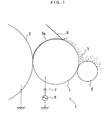
- Fig. 1 is a schematic illustration of an embodiment of a developing device in accordance with the present invention.
- a developing device 1 of this embodiment comprises a photoreceptor 2 which is a latent image carrier on which an electrostatic latent image is formed, an image developing roll 4 which carries toner 3 as a developer and conveys the same to the photoreceptor 2, a toner supply roll 5 which supplies toner 3 to the image developing roll 4, and a regulating member 6 which regulates toner 3 supplied from the toner supply roll 5 and conveyed by the image developing roll 4.
- the toner supply roll 5 having a conductive or non-conductive elastic surface is in contact with the image developing roll 4, being rotationally driven at a predetermined peripheral speed ratio, while the regulating member 6 is constantly pressed against the image developing roll 4.
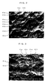
- the image developing roll 4 is composed of a metallic roll made of aluminum or aluminum alloy. At least a toner 3 carrying region (toner conveying region) of the metallic roll surface is treated with sand blast treatment, whereby a rough surface morphology is formed.
- This rough surface morphology consists of clear ridges (edges) 4b bounding adjacent recesses 4a, as shown in Fig. 2.
- At least sand blasted region of the metallic roll surface is treated with aluminum anodizing.
- the electrolysis reaction penetrates into the substance of the metallic roll, forming a relatively thin oxidation layer on the metallic roll surface.
- Al or aluminum alloy is preferable. Particularly preferable are Al-Mg based aluminum alloys, of which the most preferable examples are No. 5005 and No. 5052 alloy.
- the Al-Mg based aluminum alloys have higher abrasion resistance as compared to the other alloys, and can maintain the surface morphology of the image developing roll 4 for a longer period, while the charging property for toner 3 is improved because of the action of Mg.
- Al-Mn-Si based alloys of which the most preferable are No. 6061 and No. 6063 alloys.
- This Al-Mn-Si based alloys also have higher abrasion resistance than other alloys and can maintain the surface morphology of the image developing roll 4 for a longer period.
- the surface roughness and the surface morphology after the sand blast treatment are determined in such a manner as to obtain a uniform toner layer and a desired toner charging.
- Controlling factors for the surface roughness and the surface morphology after the sand blast treatment are type, size number, and shape of the abrasive grains.
- abrasive grains ceramic grains can be used. Among ceramic grains, particularly preferable are:
- abrasive grains used in the sand blast treatment are glass grains.
- glass grains particularly preferable is: type: soda lime glass, size number: #10 - #1200, shape: spherical.
- abrasive grains used in the sand blast treatment are metallic grains.
- metallic grains particularly preferable is: type: reduced iron, size number: #16 - #150, shape: irregular.
- Blasting conditions of abrasive grains such as nozzle diameter, distance between the nozzle and the work, air pressure, work revolution, and blasting time are determined depending on the type of the abrasive grains, in such a manner as to obtain an uniform toner layer formation (that is, an uniform toner conveyance) and desired toner charging.
- suitable conditions are:
- the metallic roll is subjected to a subsequent treatment which is not regarded as sealing treatment, in which the oxidation layer is metallized by treating it in an electrolysis solution containing metal salt.
- a subsequent treatment which is not regarded as sealing treatment, in which the oxidation layer is metallized by treating it in an electrolysis solution containing metal salt.
- suitable subsequent treatment are:
- a direct current electrolysis in an electrolysis solution containing metal salt of Ni or the like in which, for example, an oxidation layer formed by anodic oxidation in sulfuric acid is subjected to electrolysis in an electrolysis solution containing nickel sulfate + boric acid or in other electrolysis solution with a direct current.
- toner charging performance is improved because of the action of Ni, which results in decrease of background toning and toner scattering.
- a nickel acetate treatment is preferable.
- a suitable example of the nickel acetate sealing treatment is as follows:
- Metallic roll is treated in a solution containing 5 - 5.8 g/l of nickel acetate, 1 g/l of cobalt acetate, and 8 - 84 g/l of boric acid with a pH value of 5 - 6, at a temperature of 70 - 90 C for a period of 15 - 20 minutes.
- nickel acetate sealing treatment By applying this nickel acetate sealing treatment, toner charging performance is improved because of the action of Ni, which results in decrease of background toning and toner scattering.
- the oxidation layer 9 has a cell structure known as Keller's model, consisting of a thick porous layer 9 having many minute holes 9a 1 and a dense and very thin active layer 9b, as shown in Fig. 5.
- the minute holes 9a 1 have approximately cylindrical shape with a diameter of about 30 nm.
- the oxidation layer 9 as a whole has a predetermined electric resistance owing to the electrically resistant active layer 9b.
- aluminum anodizing forms an electrically resistant layer in the superficial region of a metallic roll having a relatively low electric resistance.
- the oxidation layer 9 has a predetermined hardness, which imparts a predetermined hardness to the metallic roll surface.
- the hardness of the surface of the image developing roll 4 can be further increased by performing the treatment slowly in an electrolysis solution kept at relatively low temperature.
- the oxidation layer 9 formed on the roll surface by aluminum anodizing is so thin that the oxidation layer 9 hardly influences the surface morphology previously formed by the sand blast treatment.
- the rough surface morphology formed by the sand blast treatment is mostly preserved in the surface morphology of the metallic roll after aluminum anodizing.
- a developing bias is applied to the image developing roll 4 of the developing device 1 of this embodiment, just as in conventional developing devices.
- a developing bias consisting of direct current voltage from a direct current source 7 overlapped with alternate current voltage from an alternate current source 8 is applied to the developing roll 4 of the image developing device 1 of this embodiment.
- the developing bias potential V d of the developing roller 4 is set such that its maximum value V dmax is equal with the image portion potential V on , while its minimum value V dmin is set to be higher than non-image portion potential V o .
- the developing bias V d is set at a predetermined value which is nearer to the image portion potential V on with respect to the non-image portion potential V o , and not on the opposite side of the image portion potential V on with respect to the non-image portion potential V o . In this way, particles of toner 3 on the image developing roll 4 are more effectively prevented from adhering to the non-image portion of the photoreceptor 2.
- toner 3 used in the developing device of this embodiment is formed as an non-magnetic monocomponent toner comprising toner particles 3c composed of a mother particle 3a consisting of relatively soft polyester resin, and external additives 3b consisting of relatively hard silica, adhering to the mother particle.
- the external additives include two kinds of particles, large and small, the larger particles 3b1 having diameters in a range of 30 to 50 nm and the smaller particles 3b2 having diameters of several nm.
- the diameters of smaller particles 3b2 are far smaller than the diameters of foregoing minute holes 9a 1 in the oxidation layer 9. Accordingly, the smaller particles 3b 2 in the external additives 3b can easily enter into the minute holes 9a 1 in the oxidation layer 9.
- Such a non-magnetic monocomponent toner usually includes liberated external additives 3b which are separate from the mother particles.
- a liberation ratio of the external additives is set to be 2% or more.
- toner particles comprising toner mother particles consisting of resin (C) and external additives consisting of silica (SiO 2 ) adhering to the mother particles surface are introduced into a plasma in which toner particles are excited to generate emission spectrum as shown in Figs/ 8(a) and 8(b), whereby an elementary analysis is conducted.
- the horizontal axis of the emission spectrum indicates the time axis.
- a toner particle consisting of a resinous mother particle (C) and external additives (SiO 2 ) adhering to the former is introduced into a plasma as shown in Fig. 8(a)
- both the mother particle and external additives emit lights.
- the mother particle (C) and the external additives emit lights at the same time, as they are introduced into the plasma at the same time.
- a mother particle (C) and external additives (SiO 2 ) emit lights at the same time, they are called to be in a synchronous state.
- a synchronous state of a mother particle (C) and external additives (SiO 2 ) means a state in which external additives (SiO 2 ) adhere to a mother particle (C).
- both the mother particle (C) and the external additives (SiO 2 ) emit lights just as described above.
- the mother particle (C) and the external additives (SiO 2 ) emit lights at different times as the mother particle (C) and the external additives (SiO 2 ) are introduced into the plasma at different times (for instance, the mother particle emits light earlier and the external additives emit light later when the mother particle is introduced into the plasma prior to the external additives).
- an asynchronous state of a mother particle (C) and external additives (SiO 2 ) means a state in which external additives (SiO 2 ) do not adhere to a mother particle (C).
- the height of emission signals in Figs. 8(a) and 8(b) indicate the intensities of lights, which are in proportion not to the sizes and the shapes of particles, but to the number of atoms of the respective elements (C, SiO 2 ).
- spherical particles are supposed which consist only of mother particles (C) and external additives (SiO 2 ) respectively, whose diameters represent the diameters of mother particles (C) and external additives (SiO 2 ) respectively.
- This supposed spherical particles are called equivalent particles and their particle sizes are called equivalent particle sizes. Since the external additives are so small to be detected one by one, a totaled emission intensity is converted to one equivalent particle to be used in the analysis.
- the horizontal axis indicates the equivalent particle sizes of mother particles (C) and the vertical axis indicates the equivalent particle sizes of external additives (SiO 2 ).
- the equivalent particles lying on the horizontal axis indicate asynchronous mother particles (C) without external additives (SiO 2 ) adhering to the former.
- those mother particles (C) having external additives at a lower concentration level than predetermined are regarded as asynchronous mother particle (C), and also lie on the horizontal axis.
- the equivalent particles lying on the vertical axis indicate asynchronous external additives (SiO 2 ) liberated from mother particles (C).
- the equivalent particles lying neither on horizontal nor on vertical axis indicate mother particles (C) with external additives (SiO 2 ) adhering to the former.
- the surface hardness of the surface of the image developing roll 4 is set to be lower than the hardness of external additives of toner 3. More particularly, the surface hardness of the image developing roll 4 is set relative to the hardness of external additives such that the rough surface morphology of the image developing roll 4 is scraped for a certain extent, but not scraped excessively.
- the sphericity of toner particles of toner 3 is set at 0.9 - 1 expressed in Wadell's practical sphericity, which is favorable for high fidelity visualization of high definition latent image on the latent image carrier.
- This Wadell's practical sphericity for toner 3 is a value expressed by a ratio between the diameter of a circle having an area equivalent with projected image area of a toner particle, and the diameter of a minimum circle circumscribing projected image of a toner particle.
- the Wadell's practical sphericity can be measured by means of an image processing device (manufactured by Apionix) providing an optical microscope, and its measuring procedure is described in above mentioned Japanese Unexamined Patent Publication No. H9-311544. As the measuring procedure should be readily understood by those skilled in the art by reference to the publication, the description for it is here omitted.
- toner 3 supplied by the toner supply roll 5 onto the image developing roll 4 is conveyed by the image developing roll 4 rotating counterclockwise in Fig. 1 toward the regulation member 6.
- Toner 3 which has reached to the regulation member 6 is regulated by the regulation member 6 for the conveyed amount to the photoreceptor 2, and excess toner is returned toward the supply roll 5.
- Toner 3 which has passed through the regulation member 6 forms on the image developing roll 4 a thin layer 3d of toner with a predetermined thickness.
- the thin-layered toner 3 is conveyed by the image developing roll 3 toward the photoreceptor 2, to develop a latent image on the photoreceptor 2 by forming a toner image on the photoreceptor 2.
- the rough morphology of the surface of the image developing roll 4 formed by sand blast treatment can be mostly preserved after aluminum anodizing. That is to say, the ridges in the rough morphology are sufficiently clear even after anodizing.
- the effect of clear ridges in the surface morphology of the image developing roll 4 ensure a reliable conveying of toner 3, thus improving the conveying property of the roll for toner 3.
- the preserving of the ridges formed in the sand blast treatment can increase the contact area between the image developing roll 4 and the toner particles 3. This in turn ensures a sufficient friction between the image developing roll 4 and toner particles 3, thereby effectively friction charging toner 3.
- the charging property of the roll for toner 3 can be improved.
- the oxidation layer formed by aluminum anodizing hardens the surface of the image developing roll 4, improving both abrasion resistance and the mechanical strength of the image developing roll 4.
- the surface hardness of the image developing roll 4 can be further increased by conducting anodizing slowly in an electrolysis solution kept at a relatively low temperature.
- the metallic roll 4 made of aluminum having a relatively low electric resistance can be provided with an predetermined electric resistance, because of the electrically resistant layer consisting of oxidation layer formed on the roll surface by means of anodizing.
- the electric resistance can be obtained uniformly over the anodic oxidation treated part of the metallic roll 4, as the anodic oxidation occurs uniformly over the metallic roll surface.
- the image developing roll 4 can be formed easily and at a low cost from a metallic roll having an uniform and predetermined value of electric resistance, without requiring a special material originally having a predetermined electric resistance for the manufacture of the image developing roll 4.
- the image developing roll 4 having an uniform and predetermined value of electric resistance can prevent the injection of excess charge from developing bias to toner 3. This effect is particularly important in a developing device 1 employing a contact developing system, in which a large pressure exerted by toner particles 3 nipped between the latent image carrier 2 and the image developing roll 4 promotes the injection of excess charge to toner particles 3.
- the hardness of the metallic roll 4 surface is set to be lower than the hardness of external additives of toner 3.
- Such setting of hardness brings about an effect that the rough surface of the image developing roll 4 is scraped or broken little by little by the abrasion with the external additives of toner 3, which effect suppresses the adhering of toner particles 3 onto the image developing roll 4 surface, thus preventing the occurrence of filming on the image developing roll 4.
- This effect is particularly important in a developing device employing a contact developing system, in which the regulating member 6 is in contact with the image developing roll 4, and toner is prone to adhere to the roll surface at the location where the regulating member 6 touches the image developing roll 4.
- the gradual scraping of ridges in the rough surface morphology of the image developing roll 4 surface can produce new ridges in the rough surface morphology of the image developing roll 4 surface.
- the particle diameters of the smaller particles 3b 2 of external additives 3b are set to be smaller than the diameters of the minute holes 9a 1 in the oxidation layer, so that the smaller particles 3b 2 of external additives 3b can enter into the minute holes 9a 1 to be embedded therein during toner 3 is carried and conveyed on the image developing roll 4 surface.
- the minute holes 9a 1 can be sealed by the liberated external additives 3b.
- the sealing of the minute holes 9a 1 can be achieved automatically by means of the liberated external additives 3b of toner 3 during the toner conveying. Accordingly, any special treatment for sealing the many minute holes 9a 1 is not required, or even if the special sealing treatment is required, the treatment can be simplified because of the aid from the sealing effect of the liberated external additives 3b.
- the liberation ratio of external additives is 2% or more, many minute holes 9a1 can be effectively sealed with the liberated external additives 3b.
- the intervention of the liberated external additives 3b between the toner particles 3 and the image developing roll 4 or photoreceptor 2 is facilitated, thereby suppressing the occurrence of filming on the image developing roll 4 or the photoreceptor 2.
- the sphericity of the toner particles 3 is set at a nearly spherical range of 0.9 - 1 expressed in Wadell's practical sphericity, so that toner particles 3 can rotate and slide more freely, thereby ensuring an effective recharging of toner 3.
- toner particles existing in the non-image portion of the photoreceptor 2 can be recovered more reliably, while preventing a scattering of image in the image portion of the photoreceptor 2, thus ensuring a high fidelity visualization of high fine image on the photoreceptor 2.
- the fact that the sphericity of toner 3 is high means that the shapes of the liberated external additives 3b are substantial sphere, thus ensuring smooth embedding of the liberated external additives 3b into the minute holes 9a 1 in the oxidation layer 9.
- the sealing treatment of the minute holes 9a 1 can be achieved more reliably.
- the hardness of the metallic roll 4 surface is set to be lower than the hardness of external additives of toner 3.
- Such setting of hardness brings about an effect that the rough surface of the image developing roll 4 is scraped or broken little by little by the friction with the external additives of toner 3, reliably scraping off toner 3 adhering onto the image developing roll 4.
- the adhering of toner 3 onto the image developing roll 4 can be suppressed to prevent the occurrence of filming on the image developing roll 4, while providing the rough surface with new ridges formed by scraping off of old ridges.
- the peripheral speed of the image developing roll 4 is set to be higher than the peripheral speed of the photoreceptor 2, so that toner particles 3 are effectively recharged by the rotating and sliding actions of the toner particles 3 caused by the speed difference between the rolls in the developing region where the image developing roll 4 is in contact with the photoreceptor 2. In this manner, the charge of the defectively charged toner particles can be increased. As a result, toner particles 3 adhering to the non-image portion of the photoreceptor 2 can be recovered more reliably to the image developing roll 4, while in the image portion, toner particles 3 can reliably adhere to the right locations preventing so-called image scattering caused by deviation of adhering locations of toner particles 3.
- the discharging of the developing bias from the developing roll 4 can be prevented by suitably controlling the developing bias.
- the maximum potential of the developing bias to be lower than the potential set at the non-image portion of the photoreceptor 2
- the discharging of the developing bias is effectively prevented, while also preventing the background toning caused by the toner particles 3 adhering to the non-image area of the photoreceptor 2.
- the image developing roll 4 of the developing device 1 of this embodiment can perform the foregoing three functions more reliably. Accordingly, the developing device 1 of this embodiment can yield high quality image without image defects such as mottling for a long period.
- the present invention has been described with reference to an embodiment of developing device 1 in which the present invention is applied to a contact developing system.
- the present invention is not limited however to the described embodiment but can be applied to any developing device as long as it comprises the image developing roll 4, including a non-contact system developing device in which the image developing roll 4 is not in contact with the photoreceptor 2, and a developing device in which the regulating member 6 is not in contact with the image developing roll 4.
- a non-contact system developing device in which the image developing roll 4 is not in contact with the photoreceptor 2
- the regulating member 6 is not in contact with the image developing roll 4.
- the present invention when the present invention is applied to a non-contact system developing device, the toner conveying property and the toner charging property can be improved, decreasing the toner scattering.
Applications Claiming Priority (6)
| Application Number | Priority Date | Filing Date | Title |
|---|---|---|---|
| JP2000140353 | 2000-05-12 | ||
| JP2000140354 | 2000-05-12 | ||
| JP2000140353A JP3952120B2 (ja) | 2000-05-12 | 2000-05-12 | 現像装置 |
| JP2000140354A JP2001318526A (ja) | 2000-05-12 | 2000-05-12 | 現像装置 |
| JP2000160386 | 2000-05-30 | ||
| JP2000160386A JP3633850B2 (ja) | 2000-05-30 | 2000-05-30 | 現像方法 |
Publications (3)
| Publication Number | Publication Date |
|---|---|
| EP1154334A2 true EP1154334A2 (fr) | 2001-11-14 |
| EP1154334A3 EP1154334A3 (fr) | 2004-08-04 |
| EP1154334B1 EP1154334B1 (fr) | 2007-11-28 |
Family
ID=27343361
Family Applications (1)
| Application Number | Title | Priority Date | Filing Date |
|---|---|---|---|
| EP01111217A Expired - Lifetime EP1154334B1 (fr) | 2000-05-12 | 2001-05-14 | Dispositif de développement avec rouleau avec surface rugeuse et un développateur comprenant des additives avec une taille en accord avec la structure de la-dite surface |
Country Status (3)
| Country | Link |
|---|---|
| US (1) | US6507722B2 (fr) |
| EP (1) | EP1154334B1 (fr) |
| DE (1) | DE60131594T2 (fr) |
Cited By (1)
| Publication number | Priority date | Publication date | Assignee | Title |
|---|---|---|---|---|
| EP1347345A2 (fr) * | 2002-03-07 | 2003-09-24 | Seiko Epson Corporation | Elément de support de développateur et sa production, utilisé dans un dispositif de développement, un appareil de formation d'images ou un système d'ordinateur, et notamment avec un révélateur comprenant des particules de toner pulvérisés |
Families Citing this family (6)
| Publication number | Priority date | Publication date | Assignee | Title |
|---|---|---|---|---|
| US7245928B2 (en) * | 2000-10-27 | 2007-07-17 | Cellemetry, Llc | Method and system for improved short message services |
| JP2004280068A (ja) * | 2003-02-07 | 2004-10-07 | Ricoh Co Ltd | 画像形成装置及び画像形成方法 |
| CN100444038C (zh) * | 2004-02-26 | 2008-12-17 | 京瓷美达株式会社 | 显影方法及显影装置 |
| JP2009020224A (ja) * | 2007-07-11 | 2009-01-29 | Oki Data Corp | 現像装置及び画像形成装置 |
| US9581934B2 (en) * | 2013-12-26 | 2017-02-28 | Canon Kabushiki Kaisha | Developing apparatus, developing method, image forming apparatus, and image forming method |
| US11054757B2 (en) * | 2018-09-27 | 2021-07-06 | Ricoh Company, Ltd. | Toner, image forming apparatus, image forming method, and process cartridge |
Citations (5)
| Publication number | Priority date | Publication date | Assignee | Title |
|---|---|---|---|---|
| US5387963A (en) * | 1992-12-28 | 1995-02-07 | Fuji Xerox Co., Ltd. | One-component developing device |
| US5473416A (en) * | 1992-12-04 | 1995-12-05 | Konica Corporation | Developing apparatus |
| US5659858A (en) * | 1992-12-16 | 1997-08-19 | Seiko Epson Corporation | Developing method and system |
| US5887233A (en) * | 1996-07-19 | 1999-03-23 | Fuji Xerox Co., Ltd. | Photographic developing apparatus and electrifying apparatus |
| WO1999023534A1 (fr) * | 1997-10-31 | 1999-05-14 | Sanyo Chemical Industries, Ltd. | Toner et liant pour toner |
Family Cites Families (5)
| Publication number | Priority date | Publication date | Assignee | Title |
|---|---|---|---|---|
| JPH0697809B2 (ja) * | 1988-07-12 | 1994-11-30 | 三菱電機株式会社 | 需要電力監視装置 |
| JPH0546008A (ja) * | 1991-08-09 | 1993-02-26 | Matsushita Electric Ind Co Ltd | 粉体担持体 |
| JPH0646331A (ja) * | 1992-07-24 | 1994-02-18 | Matsushita Electric Ind Co Ltd | 映像特殊効果発生装置 |
| JPH0772734A (ja) * | 1993-09-06 | 1995-03-17 | Matsushita Electric Ind Co Ltd | 電子写真装置 |
| JP2001242660A (ja) * | 2000-02-28 | 2001-09-07 | Seiko Epson Corp | 画像形成装置 |
-
2001
- 2001-05-14 EP EP01111217A patent/EP1154334B1/fr not_active Expired - Lifetime
- 2001-05-14 DE DE60131594T patent/DE60131594T2/de not_active Expired - Lifetime
- 2001-05-14 US US09/853,660 patent/US6507722B2/en not_active Expired - Fee Related
Patent Citations (5)
| Publication number | Priority date | Publication date | Assignee | Title |
|---|---|---|---|---|
| US5473416A (en) * | 1992-12-04 | 1995-12-05 | Konica Corporation | Developing apparatus |
| US5659858A (en) * | 1992-12-16 | 1997-08-19 | Seiko Epson Corporation | Developing method and system |
| US5387963A (en) * | 1992-12-28 | 1995-02-07 | Fuji Xerox Co., Ltd. | One-component developing device |
| US5887233A (en) * | 1996-07-19 | 1999-03-23 | Fuji Xerox Co., Ltd. | Photographic developing apparatus and electrifying apparatus |
| WO1999023534A1 (fr) * | 1997-10-31 | 1999-05-14 | Sanyo Chemical Industries, Ltd. | Toner et liant pour toner |
Cited By (3)
| Publication number | Priority date | Publication date | Assignee | Title |
|---|---|---|---|---|
| EP1347345A2 (fr) * | 2002-03-07 | 2003-09-24 | Seiko Epson Corporation | Elément de support de développateur et sa production, utilisé dans un dispositif de développement, un appareil de formation d'images ou un système d'ordinateur, et notamment avec un révélateur comprenant des particules de toner pulvérisés |
| EP1347345A3 (fr) * | 2002-03-07 | 2004-01-02 | Seiko Epson Corporation | Elément de support de développateur et son production, utilisé dans un dispositif de développement, un appareil de formation d'images ou un système d'ordinateur, et notamment avec un révélateur comprenant des particules de toner pulvérisés |
| US6941100B2 (en) | 2002-03-07 | 2005-09-06 | Seiko Epson Corporation | Developer bearing member, method for producing developer bearing member, developing device, image-forming apparatus, and computer system |
Also Published As
| Publication number | Publication date |
|---|---|
| US6507722B2 (en) | 2003-01-14 |
| DE60131594T2 (de) | 2008-10-23 |
| DE60131594D1 (de) | 2008-01-10 |
| EP1154334B1 (fr) | 2007-11-28 |
| EP1154334A3 (fr) | 2004-08-04 |
| US20020009313A1 (en) | 2002-01-24 |
Similar Documents
| Publication | Publication Date | Title |
|---|---|---|
| JP4732536B2 (ja) | 現像装置 | |
| US6856780B2 (en) | Method and device for developing a latent image and image forming apparatus using the same | |
| JPH11194618A (ja) | 画像形成装置 | |
| US6546222B2 (en) | Developing apparatus | |
| JP4952019B2 (ja) | 現像剤担持体及びその製造方法並びにその現像剤担持体を用いる現像装置 | |
| US6507722B2 (en) | Developing device | |
| JP4630707B2 (ja) | 現像装置およびプロセスカートリッジ及び電子写真画像形成装置 | |
| JP4545990B2 (ja) | 現像装置 | |
| EP1154332A2 (fr) | Dispositif de développement | |
| JP4378143B2 (ja) | 現像装置 | |
| JP4272723B2 (ja) | 画像形成装置 | |
| JP2001100531A (ja) | 電子写真用現像装置 | |
| US5659840A (en) | Developing method using developing electric field having back-transfer, transfer and rest steps | |
| EP2940529A1 (fr) | Appareil de formation d'image | |
| EP1235119A2 (fr) | Elément de transport de développateur, et appareil de développement et de formation d'images comprenant cet élément | |
| JP3633850B2 (ja) | 現像方法 | |
| JP3297549B2 (ja) | 現像スリーブ及び現像装置 | |
| JP2008040400A (ja) | 現像装置及びこれを用いた画像形成装置、現像剤担持体及びその製法 | |
| JP2000206776A (ja) | 現像装置 | |
| JP3952120B2 (ja) | 現像装置 | |
| JP2002351208A (ja) | 現像装置 | |
| JPH08202140A (ja) | 現像装置 | |
| JP3990922B2 (ja) | 現像剤担持部材、それを用いた画像形成装置 | |
| JPS59198480A (ja) | 現像装置 | |
| JPS61179472A (ja) | 現像装置 |
Legal Events
| Date | Code | Title | Description |
|---|---|---|---|
| PUAI | Public reference made under article 153(3) epc to a published international application that has entered the european phase |
Free format text: ORIGINAL CODE: 0009012 |
|
| AK | Designated contracting states |
Kind code of ref document: A2 Designated state(s): AT BE CH CY DE DK ES FI FR GB GR IE IT LI LU MC NL PT SE TR |
|
| AX | Request for extension of the european patent |
Free format text: AL;LT;LV;MK;RO;SI |
|
| PUAL | Search report despatched |
Free format text: ORIGINAL CODE: 0009013 |
|
| AK | Designated contracting states |
Kind code of ref document: A3 Designated state(s): AT BE CH CY DE DK ES FI FR GB GR IE IT LI LU MC NL PT SE TR |
|
| AX | Request for extension of the european patent |
Extension state: AL LT LV MK RO SI |
|
| 17P | Request for examination filed |
Effective date: 20041007 |
|
| AKX | Designation fees paid |
Designated state(s): AT BE CH CY DE DK ES FI FR GB GR IE IT LI LU MC NL PT SE TR |
|
| GRAP | Despatch of communication of intention to grant a patent |
Free format text: ORIGINAL CODE: EPIDOSNIGR1 |
|
| RTI1 | Title (correction) |
Free format text: DEVELOPING DEVICE WITH ROLL HAVING A ROUGH SURFACE AND A DEVELOPER HAVING ADDITIVES WITH A SIZE ACCORDING TO THE SURFACE STRUCTURE |
|
| GRAS | Grant fee paid |
Free format text: ORIGINAL CODE: EPIDOSNIGR3 |
|
| GRAA | (expected) grant |
Free format text: ORIGINAL CODE: 0009210 |
|
| AK | Designated contracting states |
Kind code of ref document: B1 Designated state(s): AT BE CH CY DE DK ES FI FR GB GR IE IT LI LU MC NL PT SE TR |
|
| REG | Reference to a national code |
Ref country code: GB Ref legal event code: FG4D |
|
| REG | Reference to a national code |
Ref country code: IE Ref legal event code: FG4D |
|
| REG | Reference to a national code |
Ref country code: CH Ref legal event code: EP |
|
| REF | Corresponds to: |
Ref document number: 60131594 Country of ref document: DE Date of ref document: 20080110 Kind code of ref document: P |
|
| PG25 | Lapsed in a contracting state [announced via postgrant information from national office to epo] |
Ref country code: NL Free format text: LAPSE BECAUSE OF FAILURE TO SUBMIT A TRANSLATION OF THE DESCRIPTION OR TO PAY THE FEE WITHIN THE PRESCRIBED TIME-LIMIT Effective date: 20071128 Ref country code: SE Free format text: LAPSE BECAUSE OF FAILURE TO SUBMIT A TRANSLATION OF THE DESCRIPTION OR TO PAY THE FEE WITHIN THE PRESCRIBED TIME-LIMIT Effective date: 20080228 Ref country code: LI Free format text: LAPSE BECAUSE OF FAILURE TO SUBMIT A TRANSLATION OF THE DESCRIPTION OR TO PAY THE FEE WITHIN THE PRESCRIBED TIME-LIMIT Effective date: 20071128 Ref country code: CH Free format text: LAPSE BECAUSE OF FAILURE TO SUBMIT A TRANSLATION OF THE DESCRIPTION OR TO PAY THE FEE WITHIN THE PRESCRIBED TIME-LIMIT Effective date: 20071128 Ref country code: ES Free format text: LAPSE BECAUSE OF FAILURE TO SUBMIT A TRANSLATION OF THE DESCRIPTION OR TO PAY THE FEE WITHIN THE PRESCRIBED TIME-LIMIT Effective date: 20080311 |
|
| NLV1 | Nl: lapsed or annulled due to failure to fulfill the requirements of art. 29p and 29m of the patents act | ||
| PG25 | Lapsed in a contracting state [announced via postgrant information from national office to epo] |
Ref country code: FI Free format text: LAPSE BECAUSE OF FAILURE TO SUBMIT A TRANSLATION OF THE DESCRIPTION OR TO PAY THE FEE WITHIN THE PRESCRIBED TIME-LIMIT Effective date: 20071128 |
|
| REG | Reference to a national code |
Ref country code: CH Ref legal event code: PL |
|
| PG25 | Lapsed in a contracting state [announced via postgrant information from national office to epo] |
Ref country code: AT Free format text: LAPSE BECAUSE OF FAILURE TO SUBMIT A TRANSLATION OF THE DESCRIPTION OR TO PAY THE FEE WITHIN THE PRESCRIBED TIME-LIMIT Effective date: 20071128 |
|
| ET | Fr: translation filed | ||
| PG25 | Lapsed in a contracting state [announced via postgrant information from national office to epo] |
Ref country code: DK Free format text: LAPSE BECAUSE OF FAILURE TO SUBMIT A TRANSLATION OF THE DESCRIPTION OR TO PAY THE FEE WITHIN THE PRESCRIBED TIME-LIMIT Effective date: 20071128 |
|
| PG25 | Lapsed in a contracting state [announced via postgrant information from national office to epo] |
Ref country code: BE Free format text: LAPSE BECAUSE OF FAILURE TO SUBMIT A TRANSLATION OF THE DESCRIPTION OR TO PAY THE FEE WITHIN THE PRESCRIBED TIME-LIMIT Effective date: 20071128 |
|
| PG25 | Lapsed in a contracting state [announced via postgrant information from national office to epo] |
Ref country code: PT Free format text: LAPSE BECAUSE OF FAILURE TO SUBMIT A TRANSLATION OF THE DESCRIPTION OR TO PAY THE FEE WITHIN THE PRESCRIBED TIME-LIMIT Effective date: 20080428 |
|
| PLBE | No opposition filed within time limit |
Free format text: ORIGINAL CODE: 0009261 |
|
| STAA | Information on the status of an ep patent application or granted ep patent |
Free format text: STATUS: NO OPPOSITION FILED WITHIN TIME LIMIT |
|
| 26N | No opposition filed |
Effective date: 20080829 |
|
| PG25 | Lapsed in a contracting state [announced via postgrant information from national office to epo] |
Ref country code: MC Free format text: LAPSE BECAUSE OF NON-PAYMENT OF DUE FEES Effective date: 20080531 |
|
| PG25 | Lapsed in a contracting state [announced via postgrant information from national office to epo] |
Ref country code: GR Free format text: LAPSE BECAUSE OF FAILURE TO SUBMIT A TRANSLATION OF THE DESCRIPTION OR TO PAY THE FEE WITHIN THE PRESCRIBED TIME-LIMIT Effective date: 20080229 |
|
| PG25 | Lapsed in a contracting state [announced via postgrant information from national office to epo] |
Ref country code: IE Free format text: LAPSE BECAUSE OF NON-PAYMENT OF DUE FEES Effective date: 20080514 |
|
| PG25 | Lapsed in a contracting state [announced via postgrant information from national office to epo] |
Ref country code: CY Free format text: LAPSE BECAUSE OF FAILURE TO SUBMIT A TRANSLATION OF THE DESCRIPTION OR TO PAY THE FEE WITHIN THE PRESCRIBED TIME-LIMIT Effective date: 20071128 |
|
| PG25 | Lapsed in a contracting state [announced via postgrant information from national office to epo] |
Ref country code: LU Free format text: LAPSE BECAUSE OF NON-PAYMENT OF DUE FEES Effective date: 20080514 |
|
| PG25 | Lapsed in a contracting state [announced via postgrant information from national office to epo] |
Ref country code: TR Free format text: LAPSE BECAUSE OF FAILURE TO SUBMIT A TRANSLATION OF THE DESCRIPTION OR TO PAY THE FEE WITHIN THE PRESCRIBED TIME-LIMIT Effective date: 20071128 |
|
| PG25 | Lapsed in a contracting state [announced via postgrant information from national office to epo] |
Ref country code: IT Free format text: LAPSE BECAUSE OF NON-PAYMENT OF DUE FEES Effective date: 20080531 |
|
| PGFP | Annual fee paid to national office [announced via postgrant information from national office to epo] |
Ref country code: FR Payment date: 20110523 Year of fee payment: 11 |
|
| PGFP | Annual fee paid to national office [announced via postgrant information from national office to epo] |
Ref country code: GB Payment date: 20110511 Year of fee payment: 11 |
|
| PGFP | Annual fee paid to national office [announced via postgrant information from national office to epo] |
Ref country code: DE Payment date: 20110511 Year of fee payment: 11 |
|
| GBPC | Gb: european patent ceased through non-payment of renewal fee |
Effective date: 20120514 |
|
| REG | Reference to a national code |
Ref country code: FR Ref legal event code: ST Effective date: 20130131 |
|
| REG | Reference to a national code |
Ref country code: DE Ref legal event code: R119 Ref document number: 60131594 Country of ref document: DE Effective date: 20121201 |
|
| PG25 | Lapsed in a contracting state [announced via postgrant information from national office to epo] |
Ref country code: FR Free format text: LAPSE BECAUSE OF NON-PAYMENT OF DUE FEES Effective date: 20120531 Ref country code: GB Free format text: LAPSE BECAUSE OF NON-PAYMENT OF DUE FEES Effective date: 20120514 |
|
| PG25 | Lapsed in a contracting state [announced via postgrant information from national office to epo] |
Ref country code: DE Free format text: LAPSE BECAUSE OF NON-PAYMENT OF DUE FEES Effective date: 20121201 |