EP1148554A2 - Heteroübergang-Bipolartransistor und Verfahren zur Herstellung - Google Patents
Heteroübergang-Bipolartransistor und Verfahren zur Herstellung Download PDFInfo
- Publication number
- EP1148554A2 EP1148554A2 EP01301828A EP01301828A EP1148554A2 EP 1148554 A2 EP1148554 A2 EP 1148554A2 EP 01301828 A EP01301828 A EP 01301828A EP 01301828 A EP01301828 A EP 01301828A EP 1148554 A2 EP1148554 A2 EP 1148554A2
- Authority
- EP
- European Patent Office
- Prior art keywords
- layer
- base
- emitter
- ohmic electrode
- contact layer
- Prior art date
- Legal status (The legal status is an assumption and is not a legal conclusion. Google has not performed a legal analysis and makes no representation as to the accuracy of the status listed.)
- Withdrawn
Links
Images





Classifications
-
- H—ELECTRICITY
- H10—SEMICONDUCTOR DEVICES; ELECTRIC SOLID-STATE DEVICES NOT OTHERWISE PROVIDED FOR
- H10D—INORGANIC ELECTRIC SEMICONDUCTOR DEVICES
- H10D10/00—Bipolar junction transistors [BJT]
- H10D10/01—Manufacture or treatment
- H10D10/021—Manufacture or treatment of heterojunction BJTs [HBT]
-
- H—ELECTRICITY
- H10—SEMICONDUCTOR DEVICES; ELECTRIC SOLID-STATE DEVICES NOT OTHERWISE PROVIDED FOR
- H10D—INORGANIC ELECTRIC SEMICONDUCTOR DEVICES
- H10D10/00—Bipolar junction transistors [BJT]
- H10D10/80—Heterojunction BJTs
- H10D10/821—Vertical heterojunction BJTs
-
- H—ELECTRICITY
- H10—SEMICONDUCTOR DEVICES; ELECTRIC SOLID-STATE DEVICES NOT OTHERWISE PROVIDED FOR
- H10D—INORGANIC ELECTRIC SEMICONDUCTOR DEVICES
- H10D64/00—Electrodes of devices having potential barriers
- H10D64/60—Electrodes characterised by their materials
- H10D64/62—Electrodes ohmically coupled to a semiconductor
-
- H—ELECTRICITY
- H10—SEMICONDUCTOR DEVICES; ELECTRIC SOLID-STATE DEVICES NOT OTHERWISE PROVIDED FOR
- H10D—INORGANIC ELECTRIC SEMICONDUCTOR DEVICES
- H10D62/00—Semiconductor bodies, or regions thereof, of devices having potential barriers
- H10D62/80—Semiconductor bodies, or regions thereof, of devices having potential barriers characterised by the materials
- H10D62/85—Semiconductor bodies, or regions thereof, of devices having potential barriers characterised by the materials being Group III-V materials, e.g. GaAs
Definitions
- the present invention relates to a heterojunction bipolar transistor (hereinafter, referred to as HBT) and a manufacturing method therefor.
- HBT heterojunction bipolar transistor
- the HBT is regarded as promising in the field of high-frequency devices.
- parasitic resistance can be classified roughly into emitter resistance, base resistance and collector resistance.
- the emitter resistance tends to increase together with decreasing emitter dimensions intended for higher performance. This leads to noticeable deterioration of current amplification rate and cutoff frequency of the HBT.
- the n-type emitter ohmic electrode is provided by using AuGe based metals, W or other high melting point metals, WN or other high melting point nitrides and WSi or other high melting point silicides
- the p-type base ohmic electrode is provided by using Pt, Pd, AuZn, AuBe or the like
- the n-type collector ohmic electrode is provided by using AuGe based metals. Examples of such an HBT and an ohmic electrode used therefor are shown in the following figures (1) - (3):
- the process for forming the emitter ohmic electrode 46, the base ohmic electrodes 47 and the collector ohmic electrode includes a resist formation step for forming photoresist of a pattern corresponding to the configuration of the ohmic electrodes, a metal thin film formation step for forming a metal thin film by using vapor deposition or sputtering process, and a so-called lift-off step for leaving the metal thin film only at necessary portions by removing the photoresist.
- the base ohmic electrodes 47 are formed of Pt/Ti/Pt/Au
- the emitter ohmic electrode 46 is formed of Ti/Pt/Au
- the collector ohmic electrode is formed of AuGe.
- the emitter ohmic electrode 46, the base ohmic electrodes 47 and the collector ohmic electrode cannot be formed simultaneously.
- the emitter ohmic electrode 46, the base ohmic electrodes 47 and the collector ohmic electrode need to be manufactured by different processes, making it necessary to perform the resist formation step, the metal thin film formation step and the lift-off step for each of the emitter ohmic electrode 46, the base ohmic electrodes 47 and the collector ohmic electrode.
- use of expensive materials such as Pt and Au causes the manufacturing cost to further increase.
- the emitter ohmic electrode 62 and the collector ohmic electrode 63 which are formed of AuGeNi, can be formed by one manufacturing step at the same time.
- performing heat treatment may cause the electrode metals to react nonuniformly and flocculate into island-like shapes, resulting in nonuniform ohmic contacts within the electrode regions.
- the ohmic contact resistance would not lower enough, and the emitter resistance and the collector resistance would increase. This leads to a problem that the current amplification rate and the cutoff frequency are deteriorated, in particular, because of increase in the emitter resistance.
- the emitter resistance tends to further increase by scale-down of the emitter size intended for higher performance.
- the contact resistivity of ohmic electrodes after annealing is about 1 ⁇ 10 -6 ⁇ cm 2 for p-type GaAs, but it is 1 ⁇ 10 -5 ⁇ cm 2 , one digit higher, for n-type GaAs. Therefore, when these ohmic electrodes are used for an npn-type HBT, the emitter resistance especially of n type increases, leading to a problem that the current amplification rate and the cutoff frequency are deteriorated, as in the case of (2).
- Equation (1) It can be understood from Equation (1) that decreases of the emitter resistance RE and the collector resistance RC are effective for improvement of the cutoff frequency f T .
- a decrease of the collector resistance RC can be obtained by making the collector part sufficiently thick to lower the sheet resistance of the collector. Therefore, it is the emitter resistance RE that demands special consideration. Since the emitter size will be further scaled down for higher performance in the future, a contact resistivity of 1 ⁇ 10 -6 ⁇ cm 2 or less is essential also for n-type GaAs.
- a heterojunction bipolar transistor comprising: a low-concentration n-type collector layer formed a semi-insulating substrate; a high-concentration p-type base layer formed on the collector layer; a low-concentration n-type emitter layer formed on the base layer; a base ohmic electrode which is made of a single layer or a plurality of layers and which is formed on a base protective layer that is a portion of the emitter layer; a high-concentration n-type emitter contact layer formed so as to cover regions of the emitter layer except the base protective layer; and an emitter ohmic electrode which is made of a single layer or a plurality of layers and which is formed on the emitter contact layer, further comprising:
- the base ohmic electrode is connected to the high-concentration p-type base layer through the base-use alloyed reaction layer, and the emitter ohmic electrode is connected to the higher-concentration n-type emitter contact layer through the emitter-use alloyed reaction layer.
- the base-use alloyed reaction layer extends through the base protective layer, reaching the base layer, while the emitter-use alloyed reaction layer is formed only within the emitter contact layer, not extending through the emitter contact layer.
- the emitter-use alloyed reaction layer is formed only within the higher-concentration n-type emitter contact layer and that the base-use alloyed reaction layer extends through the base protective layer to reach the high-concentration p-type base layer
- the barrier width of the junction between the high-concentration n-type emitter contact layer and the emitter-use alloyed reaction layer becomes narrow and the barrier width of the junction between the high-concentration p-type base layer and the base-use alloyed reaction layer becomes narrow, allowing the carriers to pass freely through the barriers by the tunneling effect.
- the base ohmic electrode and the emitter ohmic electrode show successful ohmic characteristics so that the emitter resistance is decreased, making is possible to improve the current amplification rate and the cutoff frequency.
- the base ohmic electrode and the emitter ohmic electrode are made of an identical material.
- the base ohmic electrode and the emitter ohmic electrode are made of an identical material, the base ohmic electrode and the emitter ohmic electrode can be manufactured by one manufacturing step. Accordingly, the number of manufacturing steps is decreased, so that the manufacturing cost can be reduced.
- the emitter contact layer is composed of a first emitter contact layer and a second emitter contact layer formed on the first emitter contact layer;
- the emitter-use alloyed reaction layer is formed only within the second emitter contact layer having a carrier concentration even higher than the carrier concentration of the first emitter contact layer, the barrier width of the junction between the higher-concentration second emitter contact layer and the emitter-use alloyed reaction layer becomes even narrower, so that the emitter ohmic electrode shows more successful ohmic characteristics. Accordingly, the resistance of the emitter ohmic electrode, i.e., the emitter resistance is decreased, making is possible to improve the current amplification rate and the cutoff frequency.
- the collector layer and the base layer are formed of GaAs and the emitter layer and the base protective layer are formed of AlGaAs.
- the arrangement that the collector layer and the base layer are formed of GaAs while the emitter layer and the base protective layer are formed of AlGaAs is desirable for improvement of the current amplification rate and the cutoff frequency.
- the first emitter contact layer is formed of GaAs and the second emitter contact layer is formed of InGaAs.
- the arrangement that the first emitter contact layer is formed of GaAs while the second emitter contact layer is formed of InGaAs is desirable for improvement of the current amplification rate and the cutoff frequency.
- the base ohmic electrode and the emitter ohmic electrode, or a lowermost layer of the base ohmic electrode and a lowermost layer of the emitter ohmic electrode are made of Pt; and the base-use alloyed reaction layer and the emitter-use alloyed reaction layer contain Pt.
- the base ohmic electrode and the emitter ohmic electrode, or the lowermost layer of the base ohmic electrode and the lowermost layer of the emitter ohmic electrode are made of Pt, while the base-use alloyed reaction layer and the emitter-use alloyed reaction layer contain Pt. This is desirable for improvement of the current amplification rate and the cutoff frequency.
- the electrode material is stacked on the emitter contact layer and the base protective layer so as to be thinner than the film thickness of the second emitter contact layer. Thereafter, the electrode material is subjected to a heat treatment, by which a base ohmic electrode is formed on the base protective layer and an emitter ohmic electrode is formed on the second emitter contact layer. In this process, a base-use alloyed reaction layer is formed under the base ohmic electrode, and an emitter-use alloyed reaction layer is formed under the emitter ohmic electrode.
- the base-use alloyed reaction layer extends through the base protective layer, reaching the high-concentration p-type base layer, while the emitter-use alloyed reaction layer is formed only within the high-concentration n-type emitter contact layer.
- the film thickness of the electrode material thinner than the film thickness of the second emitter contact layer, it becomes possible to make the base-use alloyed reaction layer extend up to the high-concentration p-type base layer and besides to form the emitter-use alloyed reaction layer only within the high-concentration n-type emitter contact layer.
- the base ohmic electrode and the emitter ohmic electrode can be improved in contact.
- the film thickness of the second emitter contact layer is set to three or more times the film thickness of the electrode material Pt.
- the emitter-use alloyed reaction layer to be formed by subjecting the electrode material to the heat treatment can be prevented from extending through the second emitter contact layer.
- the film thickness of the electrode material is within a range defined by a following relational expression: (film thickness of the base protective layer ⁇ 1/2) ⁇ film thickness of the electrode material before heat treatment ⁇ ⁇ (film thickness of the base protective layer + film thickness of the base layer ) ⁇ 1/3 ⁇ .
- the base-use alloyed reaction layer to be formed by the heat treatment extends through the base layer so as to reach the collector layer.
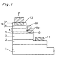
- Fig. 1 is a schematic sectional view of an HBT according to an embodiment of the present invention.
- the HBT as shown in Fig. 1, has a high-concentration n-type GaAs collector contact layer 2 formed on a semi-insulating GaAs substrate 1 as a semi-insulating substrate, a low-concentration n-type GaAs collector layer 3 formed on a collector formation region in the collector contact layer 2, a high-concentration p-type GaAs base layer 4 formed on the collector layer 3, a low-concentration n-type AlGaAs emitter layer 5 formed on the base layer 4, a base ohmic electrode 10 of Pt/Ti/Pt/Au formed on a low-concentration n-type AlGaAs base protective layer 5a which is a portion of the emitter layer 5, a high-concentration n-type emitter contact layer 14 formed so as to cover regions of the emitter layer 5 except the base protective layer 5a, and an emitter ohmic electrode 9 of Pt
- the emitter contact layer 14 is composed of a first emitter contact layer 6, and a second emitter contact layer 7 formed on the first emitter contact layer 6.
- the first emitter contact layer 6 is made of GaAs and the second emitter contact layer 7 is made of InGaAs.
- the first emitter contact layer 6 and the second emitter contact layer 7 are both high in concentration, where the second emitter contact layer 7 is higher in carrier concentration than the first emitter contact layer 6.
- a Pt alloyed reaction layer 13 As a base-use alloyed reaction layer. This alloyed reaction layer 13 extends through the base protective layer 5a, reaching the base layer 4. Further, under the emitter ohmic electrode 9 is formed a Pt alloyed reaction layer 12 as an emitter-use alloyed reaction layer. This alloyed reaction layer 12 is formed only within the second emitter contact layer 7.
- the base ohmic electrode 10 is connected to the high-concentration p-type base layer 4 through the Pt alloyed reaction layer 13, and the emitter ohmic electrode 9 is connected to the higher-concentration second emitter contact layer 7 through the Pt alloyed reaction layer 12.
- the Pt alloyed reaction layer 13 under the base ohmic electrode 10 extends through the base protective layer 5a, reaching the base layer 4, while the Pt alloyed reaction layer 12 under the emitter ohmic electrode 9 is formed only within the second emitter contact layer 7, not extending through the second emitter contact layer 7.
- the Pt alloyed reaction layer 13 under the base ohmic electrode 10 extends through the base protective layer 5a to reach the high-concentration p-type base layer 4 and that the Pt alloyed reaction layer 12 under the emitter ohmic electrode 9 is formed only within the higher-concentration second emitter contact layer 7, the barrier width of the junction between the base layer 4 and the alloyed reaction layer 13 becomes narrow and the barrier width of the junction between the second emitter contact layer 7 and the alloyed reaction layer 12 becomes even narrower, allowing the carriers to pass freely through the barriers by the tunneling effect. Accordingly, the base ohmic electrode 10 and the emitter ohmic electrode 9 show more successful ohmic characteristics so that the emitter resistance is further decreased, making is possible to improve the current amplification rate and the cutoff frequency.
- This HBT is manufactured as follows.
- a high-concentration n-type GaAs layer 102 (concentration: 5.0 ⁇ 10 18 cm -3 , thickness: 500 nm), a low-concentration n-type GaAs layer 103 (concentration: 3.0 ⁇ 10 17 cm -3 , thickness: 700 nm), a high-concentration p-type GaAs layer 104 (concentration: 1.0 ⁇ 10 19 cm -3 , thickness: 100 nm), a low-concentration n-type AlGaAs layer 105 (Al composition ratio: 0.35, concentration: 5.0 ⁇ 10 17 cm -3 , thickness: 200 nm), a high-concentration n-type GaAs layer 106 (concentration: 5.0 ⁇ 10 18 cm -3 , thickness: 100 nm), and a high-concentration n-type InGaAs layer 107 (In composition ratio: 0.6, concentration: 2.0 ⁇ 10 19
- the second emitter contact layer 7 and the first emitter contact layer 6 are formed, while part of the n-type AlGaAs layer 105 is etched, by which the AlGaAs layer 105 is formed into an AlGaAs layer 205.
- a 50 nm thick n-type AlGaAs layer 205a is formed.
- the etching time is set with care given to the fact that the etching rate differs among the high-concentration n-type InGaAs layer 107, the high-concentration n-type GaAs layer 106 and the n-type AlGaAs layer 105.
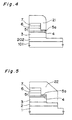
- a photoresist pattern 21 shown in Fig. 4 is formed so as to cover the second emitter contact layer 7 and part of the AlGaAs layer 205a.
- This high-concentration n-type GaAs layer 202 has part of the surface exposed.
- a photoresist pattern 22 shown in Fig. 5 is formed so as to cover the second emitter contact layer 7, the base protective layer 5a and part of the high-concentration n-type GaAs layer 202.
- a photoresist pattern 23 is formed, and AuGe (thickness: 100 nm), Ni (thickness: 10 nm), Au(thickness: 100 nm) are continuously deposited by using an evaporator.
- AuGe thinness: 100 nm
- Ni thinness: 10 nm
- Au(thickness: 100 nm) are continuously deposited by using an evaporator.
- a metal thin film 30 made of AuGe, Ni and Au is formed on the photoresist pattern 23 and on the exposed part of the collector contact layer 2, a metal thin film 30 made of AuGe, Ni and Au is formed.
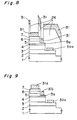
- the photoresist pattern 23 is removed, by which only a necessary portion 30a of the metal thin film 30 is left as shown in Fig. 7.
- such a photoresist pattern 24 that desired portions of the second emitter contact layer 7 and the base protective layer 5a are exposed are formed.
- Pt (thickness: 30 nm), Ti (thickness: 50 nm), Pt (thickness : 50 nm) and Au (thickness: 100 nm) as metal materials are continuously deposited by using an EB (Electron Beam) evaporator, by which a metal thin film 31 made of Pt, Ti, Pt and Au is formed.
- the photoresist pattern 24 is peeled off, by which only necessary portions 31a, 31b of the metal thin film 31 are left as shown in Fig. 9.
- a collector ohmic electrode 11 a base ohmic electrode 10 and an emitter ohmic electrode 9 are formed as shown in Fig. 1.
- Pt is diffused from the portions 31a, 31b of the metal thin film 31 into the base protective layer 5a and the second emitter contact layer 7.
- a Pt alloyed reaction layer 13 is formed under the base ohmic electrode 10
- a Pt alloyed reaction layer 12 is formed under the emitter ohmic electrode 9.
- the base ohmic electrode 10 is made of Pt/Ti/Pt/Au and that the emitter ohmic electrode 9 is made of Pt/Ti/Pt/Au
- the base ohmic electrode 10 and the emitter ohmic electrode 9 can be formed by one manufacturing step. As a result of this, the number of manufacturing steps is suppressed to a small one, so that the manufacturing cost can be reduced.
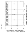
- Fig. 10 is a view showing the ratios of thicknesses of the Pt alloyed reaction layers 12, 13 formed under the emitter ohmic electrode 9 and the base ohmic electrode 10 by the heat treatment to the Pt film thicknesses before the heat treatment.
- the heat treatment is performed at 380°C. This is based on the fact that a heat treatment temperature of 350°C - 400°C is required when the collector ohmic electrode 11 to be formed on the collector contact layer 2 is made of AuGe based metal, which is widely used, and the fact that it is intended to perform both heat treatments for forming the collector ohmic electrode 11 and for forming the base ohmic electrode 10 and the emitter ohmic electrode 9 at one time.
- the film thickness of this base protective layer 5a should have a film thickness that satisfies the function as a protective layer and that fulfills a complete depletion in device operation. With considerations given to this, it is necessary to first determine the film thickness of the base protective layer 5a and then determine the film thickness of Pt that makes the lowermost layers of the emitter ohmic electrode 9 and the base ohmic electrode 10.
- Fig. 11 is a graph showing the relationship between the film thickness of Pt before heat treatment and the contact resistivity of the base ohmic electrode 10 after heat treatment.
- the film thickness of the base protective layer 5a is varied as 20 nm, 50 nm and 80 nm.
- the film thickness of the base layer 4 is 100 nm and a 380°C heat treatment is performed for 2 minutes.
- the film thickness of Pt before heat treatment that makes the lowermost layer of the base ohmic electrode 10 is less than 1/2 of the film thickness of the base protective layer 5a, the contact resistivity of the base ohmic electrode 10 to be formed by the subsequent heat treatment increases. Also, if the film thickness of Pt before heat treatment that makes the lowermost layer of the base ohmic electrode 10 is thicker than 1/3 of ⁇ film thickness of base protective layer 5a + film thickness of base layer 4 ⁇ , then the alloyed reaction layer 13 to be formed by the subsequent heat treatment penetrates through the base layer 4 to reach the collector layer 3. This means that a metal penetrates through the PN junction plane of base and collector, which incurs a major fault as a transistor.
- the contact resistivity of the base ohmic electrode 10 can be reduced and moreover the Pt alloyed reaction layer 13 formed by heat treatment can be prevented from penetrating through the base layer 4 by setting the film thickness of Pt before heat treatment that makes the lowermost layers of the base ohmic electrode 10 and the emitter ohmic electrode 9 to within the range defined by the following relational expression: (film thickness of the base protective layer 5a ⁇ 1/2) ⁇ film thickness of the Pt before heat treatment ⁇ ⁇ (film thickness of the base protective layer + film thickness of the base layer) ⁇ 1/3 ⁇
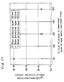
- Fig. 12 shows the heat treatment dependence of the contact resistivity of the emitter ohmic electrode 9 subjected to excessive heat treatment and the heat treatment time.
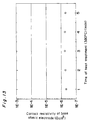
- Fig. 13 shows the heat treatment dependence of the contact resistivity of the base ohmic electrode 10 subjected to excessive heat treatment and the heat treatment time.
- the contact resistivities of the emitter ohmic electrode 9 and the base ohmic electrode 10 are on the order of 10 -7 ⁇ cm 2 regardless of the time of heat treatment. Accordingly, it can be understood that successful ohmic contacts are obtained and that the ohmic electrodes are stable thermally as well.
- the emitter structure is a one-finger structure in this embodiment, the structure may also be a so-called multi-finger structure in which a plurality of emitter fingers.
- the film thickness of the base protective layer 5a has been set to 50 nm. This film thickness of the base protective layer 5a is such an example that the function as a protective layer is satisfied and that a complete depletion is fulfilled in device operation.
- the emitter ohmic electrode 9 and the base ohmic electrode 10 have been formed each of a plurality of layers, the emitter ohmic electrode and the base ohmic electrode may also be formed each of a single layer.
Landscapes
- Bipolar Transistors (AREA)
- Electrodes Of Semiconductors (AREA)
Applications Claiming Priority (2)
| Application Number | Priority Date | Filing Date | Title |
|---|---|---|---|
| JP2000118231 | 2000-04-19 | ||
| JP2000118231A JP2001308103A (ja) | 2000-04-19 | 2000-04-19 | ヘテロ接合バイポーラトランジスタおよびその製造方法 |
Publications (2)
| Publication Number | Publication Date |
|---|---|
| EP1148554A2 true EP1148554A2 (de) | 2001-10-24 |
| EP1148554A3 EP1148554A3 (de) | 2003-10-08 |
Family
ID=18629411
Family Applications (1)
| Application Number | Title | Priority Date | Filing Date |
|---|---|---|---|
| EP01301828A Withdrawn EP1148554A3 (de) | 2000-04-19 | 2001-02-28 | Heteroübergang-Bipolartransistor und Verfahren zur Herstellung |
Country Status (4)
| Country | Link |
|---|---|
| US (1) | US6683332B2 (de) |
| EP (1) | EP1148554A3 (de) |
| JP (1) | JP2001308103A (de) |
| TW (1) | TW479362B (de) |
Cited By (3)
| Publication number | Priority date | Publication date | Assignee | Title |
|---|---|---|---|---|
| US7918714B2 (en) | 2005-03-10 | 2011-04-05 | Infineon Technologies Ag | Methods for treating wafers on assembly carriers |
| DE102005007821B4 (de) | 2005-02-21 | 2014-08-21 | Infineon Technologies Ag | Vorrichtung mit einem Montageträger |
| CN106683993A (zh) * | 2016-12-26 | 2017-05-17 | 厦门市三安光电科技有限公司 | 一种晶体管欧姆接触电极的制备方法 |
Families Citing this family (6)
| Publication number | Priority date | Publication date | Assignee | Title |
|---|---|---|---|---|
| US7001820B1 (en) | 2004-03-08 | 2006-02-21 | Matsushita Electric Industrial Co., Ltd. | Heterojunction bipolar transistor and method for fabricating the same |
| JP2006073692A (ja) * | 2004-09-01 | 2006-03-16 | Matsushita Electric Ind Co Ltd | ヘテロ接合バイポーラトランジスタおよびその製造方法 |
| JP2006303244A (ja) | 2005-04-21 | 2006-11-02 | Matsushita Electric Ind Co Ltd | ヘテロ接合バイポーラトランジスタ及びその製造方法 |
| US8395237B2 (en) * | 2008-10-21 | 2013-03-12 | Nec Corporation | Group nitride bipolar transistor |
| JP5628681B2 (ja) | 2008-10-21 | 2014-11-19 | ルネサスエレクトロニクス株式会社 | バイポーラトランジスタ |
| JP2019054120A (ja) * | 2017-09-15 | 2019-04-04 | 株式会社村田製作所 | バイポーラトランジスタ及び高周波パワーアンプモジュール |
Citations (1)
| Publication number | Priority date | Publication date | Assignee | Title |
|---|---|---|---|---|
| JPH10154714A (ja) * | 1996-11-21 | 1998-06-09 | Sharp Corp | 化合物半導体装置およびその製造方法 |
Family Cites Families (8)
| Publication number | Priority date | Publication date | Assignee | Title |
|---|---|---|---|---|
| US5106771A (en) * | 1991-06-05 | 1992-04-21 | At&T Bell Laboratories | GaAs MESFETs with enhanced Schottky barrier |
| US5682046A (en) | 1993-08-12 | 1997-10-28 | Fujitsu Limited | Heterojunction bipolar semiconductor device and its manufacturing method |
| US5442194A (en) * | 1994-01-07 | 1995-08-15 | Texas Instruments Incorporated | Room-temperature tunneling hot-electron transistor |
| JPH08222526A (ja) | 1995-02-15 | 1996-08-30 | Matsushita Electric Ind Co Ltd | P・n型同一オーミック材料及びその製造方法 |
| JP3294461B2 (ja) | 1995-03-14 | 2002-06-24 | シャープ株式会社 | ヘテロ接合バイポーラトランジスタとその製造方法 |
| EP0810646A3 (de) | 1996-05-13 | 1998-01-14 | Trw Inc. | Verfahren zur Herstellung eines Heterobipolartransistors mit sehr hohem Verstärkungsfaktor |
| JP3594482B2 (ja) | 1998-04-02 | 2004-12-02 | 三菱電機株式会社 | ヘテロ接合バイポーラトランジスタ |
| US5907165A (en) | 1998-05-01 | 1999-05-25 | Lucent Technologies Inc. | INP heterostructure devices |
-
2000
- 2000-04-19 JP JP2000118231A patent/JP2001308103A/ja active Pending
-
2001
- 2001-02-05 US US09/775,593 patent/US6683332B2/en not_active Expired - Fee Related
- 2001-02-15 TW TW090103402A patent/TW479362B/zh not_active IP Right Cessation
- 2001-02-28 EP EP01301828A patent/EP1148554A3/de not_active Withdrawn
Patent Citations (1)
| Publication number | Priority date | Publication date | Assignee | Title |
|---|---|---|---|---|
| JPH10154714A (ja) * | 1996-11-21 | 1998-06-09 | Sharp Corp | 化合物半導体装置およびその製造方法 |
Cited By (4)
| Publication number | Priority date | Publication date | Assignee | Title |
|---|---|---|---|---|
| DE102005007821B4 (de) | 2005-02-21 | 2014-08-21 | Infineon Technologies Ag | Vorrichtung mit einem Montageträger |
| US7918714B2 (en) | 2005-03-10 | 2011-04-05 | Infineon Technologies Ag | Methods for treating wafers on assembly carriers |
| US8753176B2 (en) | 2005-03-10 | 2014-06-17 | Infineon Technologies Ag | Device for treating wafers on assembly carriers |
| CN106683993A (zh) * | 2016-12-26 | 2017-05-17 | 厦门市三安光电科技有限公司 | 一种晶体管欧姆接触电极的制备方法 |
Also Published As
| Publication number | Publication date |
|---|---|
| EP1148554A3 (de) | 2003-10-08 |
| US6683332B2 (en) | 2004-01-27 |
| US20010046747A1 (en) | 2001-11-29 |
| TW479362B (en) | 2002-03-11 |
| JP2001308103A (ja) | 2001-11-02 |
Similar Documents
| Publication | Publication Date | Title |
|---|---|---|
| US6399971B1 (en) | Semiconductor device and method for fabricating the same | |
| EP2001052A2 (de) | Halbleiterbauelement und Herstellungsverfahren dafür | |
| CN1988172B (zh) | 异质结双极晶体管 | |
| EP0507454A1 (de) | Heterojunction-Bipolartransistor und dessen Herstellungsverfahren | |
| US6462362B1 (en) | Heterojunction bipolar transistor having prevention layer between base and emitter | |
| US6683332B2 (en) | Heterojunction bipolar transistor and manufacturing method therefor including electrode alloyed reaction layers | |
| US7449729B2 (en) | Heterojunction bipolar transistor and method for fabricating the same | |
| CN100369221C (zh) | 异质结双极晶体管及其制造方法 | |
| US20040016941A1 (en) | Hetero-junction bipolar transistor and a manufacturing method of the same | |
| US7001820B1 (en) | Heterojunction bipolar transistor and method for fabricating the same | |
| US20060284212A1 (en) | Hetero-junction bipolar transistor and manufacturing method thereof | |
| JP3874919B2 (ja) | 化合物半導体装置 | |
| JP3358901B2 (ja) | 化合物半導体装置の製造方法 | |
| JP4092597B2 (ja) | 半導体装置及びその製造方法 | |
| JP4405060B2 (ja) | ヘテロ接合型バイポーラトランジスタ | |
| JP2000311902A (ja) | 化合物半導体装置及びその製造方法 | |
| JP3624357B2 (ja) | ヘテロ接合バイポーラトランジスタの製造方法 | |
| KR100352375B1 (ko) | 이종접합 쌍극자 트랜지스터의 제조방법 | |
| JP2005159112A (ja) | 半導体装置および半導体装置の製造方法 | |
| JP2005294804A (ja) | ヘテロ接合バイポーラトランジスタ及びその製造方法 | |
| JP3857609B2 (ja) | 化合物半導体装置の製造方法 | |
| JP4364628B2 (ja) | 半導体装置の製造方法 | |
| CN119653792A (zh) | 异质结双极型晶体管及其形成方法 | |
| JPH11330087A (ja) | ヘテロ接合バイポーラトランジスタ及びその製造方法 | |
| JP3321229B2 (ja) | 半導体装置 |
Legal Events
| Date | Code | Title | Description |
|---|---|---|---|
| PUAI | Public reference made under article 153(3) epc to a published international application that has entered the european phase |
Free format text: ORIGINAL CODE: 0009012 |
|
| AK | Designated contracting states |
Kind code of ref document: A2 Designated state(s): AT BE CH CY DE DK ES FI FR GB GR IE IT LI LU MC NL PT SE TR |
|
| AX | Request for extension of the european patent |
Free format text: AL;LT;LV;MK;RO;SI |
|
| PUAL | Search report despatched |
Free format text: ORIGINAL CODE: 0009013 |
|
| AK | Designated contracting states |
Kind code of ref document: A3 Designated state(s): AT BE CH CY DE DK ES FI FR GB GR IE IT LI LU MC NL PT SE TR |
|
| AX | Request for extension of the european patent |
Extension state: AL LT LV MK RO SI |
|
| 17P | Request for examination filed |
Effective date: 20040121 |
|
| AKX | Designation fees paid |
Designated state(s): DE FR GB |
|
| 17Q | First examination report despatched |
Effective date: 20071128 |
|
| STAA | Information on the status of an ep patent application or granted ep patent |
Free format text: STATUS: THE APPLICATION IS DEEMED TO BE WITHDRAWN |
|
| 18D | Application deemed to be withdrawn |
Effective date: 20080409 |