EP1139425A2 - DRAM-Speicherzellenfeld mit n- und p-Kanal-Transistoren - Google Patents
DRAM-Speicherzellenfeld mit n- und p-Kanal-Transistoren Download PDFInfo
- Publication number
- EP1139425A2 EP1139425A2 EP01105818A EP01105818A EP1139425A2 EP 1139425 A2 EP1139425 A2 EP 1139425A2 EP 01105818 A EP01105818 A EP 01105818A EP 01105818 A EP01105818 A EP 01105818A EP 1139425 A2 EP1139425 A2 EP 1139425A2
- Authority
- EP
- European Patent Office
- Prior art keywords
- selection transistor
- channel
- active
- word line
- memory cell
- Prior art date
- Legal status (The legal status is an assumption and is not a legal conclusion. Google has not performed a legal analysis and makes no representation as to the accuracy of the status listed.)
- Withdrawn
Links
Images







Classifications
-
- H—ELECTRICITY
- H10—SEMICONDUCTOR DEVICES; ELECTRIC SOLID-STATE DEVICES NOT OTHERWISE PROVIDED FOR
- H10B—ELECTRONIC MEMORY DEVICES
- H10B12/00—Dynamic random access memory [DRAM] devices
- H10B12/30—DRAM devices comprising one-transistor - one-capacitor [1T-1C] memory cells
- H10B12/31—DRAM devices comprising one-transistor - one-capacitor [1T-1C] memory cells having a storage electrode stacked over the transistor
-
- H—ELECTRICITY
- H10—SEMICONDUCTOR DEVICES; ELECTRIC SOLID-STATE DEVICES NOT OTHERWISE PROVIDED FOR
- H10B—ELECTRONIC MEMORY DEVICES
- H10B12/00—Dynamic random access memory [DRAM] devices
- H10B12/30—DRAM devices comprising one-transistor - one-capacitor [1T-1C] memory cells
-
- H—ELECTRICITY
- H10—SEMICONDUCTOR DEVICES; ELECTRIC SOLID-STATE DEVICES NOT OTHERWISE PROVIDED FOR
- H10B—ELECTRONIC MEMORY DEVICES
- H10B12/00—Dynamic random access memory [DRAM] devices
- H10B12/01—Manufacture or treatment
- H10B12/02—Manufacture or treatment for one transistor one-capacitor [1T-1C] memory cells
- H10B12/05—Making the transistor
-
- H—ELECTRICITY
- H10—SEMICONDUCTOR DEVICES; ELECTRIC SOLID-STATE DEVICES NOT OTHERWISE PROVIDED FOR
- H10B—ELECTRONIC MEMORY DEVICES
- H10B12/00—Dynamic random access memory [DRAM] devices
- H10B12/30—DRAM devices comprising one-transistor - one-capacitor [1T-1C] memory cells
- H10B12/37—DRAM devices comprising one-transistor - one-capacitor [1T-1C] memory cells the capacitor being at least partially in a trench in the substrate
-
- H—ELECTRICITY
- H10—SEMICONDUCTOR DEVICES; ELECTRIC SOLID-STATE DEVICES NOT OTHERWISE PROVIDED FOR
- H10B—ELECTRONIC MEMORY DEVICES
- H10B12/00—Dynamic random access memory [DRAM] devices
- H10B12/30—DRAM devices comprising one-transistor - one-capacitor [1T-1C] memory cells
- H10B12/39—DRAM devices comprising one-transistor - one-capacitor [1T-1C] memory cells the capacitor and the transistor being in a same trench
- H10B12/395—DRAM devices comprising one-transistor - one-capacitor [1T-1C] memory cells the capacitor and the transistor being in a same trench the transistor being vertical
-
- H—ELECTRICITY
- H10—SEMICONDUCTOR DEVICES; ELECTRIC SOLID-STATE DEVICES NOT OTHERWISE PROVIDED FOR
- H10D—INORGANIC ELECTRIC SEMICONDUCTOR DEVICES
- H10D84/00—Integrated devices formed in or on semiconductor substrates that comprise only semiconducting layers, e.g. on Si wafers or on GaAs-on-Si wafers
- H10D84/80—Integrated devices formed in or on semiconductor substrates that comprise only semiconducting layers, e.g. on Si wafers or on GaAs-on-Si wafers characterised by the integration of at least one component covered by groups H10D12/00 or H10D30/00, e.g. integration of IGFETs
- H10D84/82—Integrated devices formed in or on semiconductor substrates that comprise only semiconducting layers, e.g. on Si wafers or on GaAs-on-Si wafers characterised by the integration of at least one component covered by groups H10D12/00 or H10D30/00, e.g. integration of IGFETs of only field-effect components
- H10D84/83—Integrated devices formed in or on semiconductor substrates that comprise only semiconducting layers, e.g. on Si wafers or on GaAs-on-Si wafers characterised by the integration of at least one component covered by groups H10D12/00 or H10D30/00, e.g. integration of IGFETs of only field-effect components of only insulated-gate FETs [IGFET]
- H10D84/85—Complementary IGFETs, e.g. CMOS
Definitions
- the present invention relates to a semiconductor memory, which has memory cells with capacitors and transistors.
- DRAM Dynamic Random Access Memory
- memory cells that have a storage capacitor and include a selection transistor.
- the control transistor becomes suitable control voltages at the gate controlled so that a current flow between the source and the drain region through the channel of the selection transistor is switched on and off.
- bit lines In addition to the bit line, there are usually other bit lines arranged.
- the circuit concept "Folded Bit Line” is used two adjacent bit lines with two inputs one Sense amplifier are connected.
- the sense amplifier is acting it is usually two connected inverters that compare the two neighboring bit lines and evaluate.
- the word line runs across the two Bit lines and a selection transistor open when applied a suitable control voltage to the word line the charge stored in the storage capacitor the first bit line flows.
- the word line is here as a passing wordline designated.
- the second bit line only serves as a reference for the first bit line on which the charge of the storage capacitor flows.
- the size of a memory cell is always larger than or equal to 8F 2 .
- the n-channel transistor opens, and the p-channel transistor blocks, so that Memory cell to be read out with the n-channel transistor and the bit line with the p-channel transistors as a reference can be used.
- An embodiment of the invention provides that at least one of the storage capacitors is a trench capacitor.
- the formation of a storage capacitor as a trench capacitor has the advantage that the storage capacitor saves space can be formed with a large capacity. Farther are usually used to form trench capacitors known methods can be used.
- At least one of the storage capacitors is a stacked capacitor is.
- Stacked capacitors also called stacked capacitors, represent another option, the storage capacitor with a large capacity in a space-saving arrangement to manufacture.
- trench isolation and the isolation layer the first selection transistor from the second selection transistor isolate. This is the compact arrangement of p-channel transistors and n-channel transistors.
- a first bit line is connected to the first memory cell and a second bit line to the second memory cell and the first bit line and the second bit line are connected to a sense amplifier.
- the connection of a sense amplifier to the first bit line, which is connected to n-channel transistors, and to the second bit line, which is connected to p-channel transistors, advantageously enables the concept "folded bit line" for memory cell sizes below 8F 2nd
- An advantageous embodiment of the invention provides that for a first word line voltage, the first selection transistor and block the second selection transistor.
- the advantage lies in the fact that both the first storage capacitor as well as the second storage capacitor which is stored in their Maintain charge because both transistors block.
- the first selection transistor opens for a second word line voltage that is larger than the first word line voltage. By doing this it is possible to open the first selection transistor to read the information stored in the first memory cell.
- the second selection transistor opens for a third word line voltage that is smaller than the first word line voltage.
- the third Word line voltage is possible in the second memory cell read out stored information.
- the gate material for the first selection transistor and / or for the second selection transistor a doped with polysilicon is used.
- the polysilicon By doping the polysilicon the threshold voltage of the first selection transistor and the second selection transistor. Thereby can be achieved, for example, that both the first selection transistor as well as the second selection transistor for the block first word line voltage.
- germanium is used as the dopant becomes. With the use of germanium as a dopant the threshold voltages of p- and n-channel transistors set symmetrically to zero. This is for Example advantageous if a symmetrical operating voltage should be used.
- a further development of the invention provides that for connection of the first storage capacitor with a first source doping region of the first selection transistor and / or for connection of the second storage capacitor with a second Source doping region of the second selection transistor is a silicide is used. Since the one source doping region is p-doped and the other source doping region is n-doped, one Silicide can be used to connect both doping regions, without forming a pn junction, which is for a voltage constellation would have a blocking effect.
- the first memory cell is provided to form on an SOI substrate.
- An SOI substrate enables the arrangement of p-channel transistors in an advantageous manner and n-channel transistors in close proximity.
- the p-channel transistors and n-channel transistors become without an SOI substrate usually by biased in the reverse direction pn junctions isolated from each other. Because this is very is space-consuming means using an SOI substrate, in which an insulating silicon oxide layer for Isolation of n-channel transistors and p-channel transistors enormous space savings can be used.
- first memory cell and the second memory cell with trench isolation from one another are isolated.
- trench isolation also STI (Shallow Trench Isolation) allows another Space saving, since neighboring transistors and doping regions can be isolated from each other.
- a conductive layer between the trench isolation and an insulation layer of the SOI substrate arranged a conductive layer.
- the usual way is the channel area of transistors on an SOI substrate are formed, not connected because of the bulk contact prevented by the insulation layer of the SOI substrate becomes.
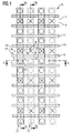
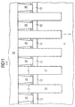
- FIG. 1 shows the top view of a memory cell array 13 shown.
- the memory cell array 13 is on a substrate 1 formed. This is, for example, an SOI substrate (Silicon on Insulator), which is a buried insulation layer 12 has.
- the active n-channel region 3 is, for example, weakly p-doped, the active p-channel region is weakly n-doped.
- About the active n-channel region 3 and the active p-channel region 4 run a first word line 9 and a second word line 10.
- Das active n-channel area 3 and the active p-channel area 4 isolated from one another by trench insulation 26.
- active n-channel area is a first memory cell 14 from a first selection transistor 16 and a first Storage capacitor 18 formed. Furthermore is a first Bit line contact 7 and an n-channel capacitor connection 5 in the active n-channel region 3.
- active p-channel area 4 is a second memory cell 15 with a second selection transistor 17 and a second storage capacitor 19 arranged.
- second bit line connection 8 and a p-channel capacitor connection 6 shown.
- the bit lines 22, 23 run across the word lines 9, 10, 11 and the first bit line 22 runs over adjacent active n-channel regions 3 and the second bit line 23 runs over adjacent active p-channel regions 4.
- section line BBn through the active n-channel regions 3
- section line BBp through the active p-channel regions 4
- section line AA in the direction of development the word lines 9, 10, 11 alternately through active n-channel areas and active p-channel regions.
- the n-channel capacitor connection 5 and the p-channel capacitor connection 6 serve to connect a stacked capacitor.
- the trench capacitors 20 can be arranged below the n-channel capacitor connection 5 and below the p-channel capacitor connection 6.
- a sense amplifier is connected to the first bit line 22 and the second bit line 23, for example. If a first word line voltage 29 is applied to the first word line 9, it is provided that the first selection transistor 16 and the second selection transistor 17 both block, so that the first memory cell 14 and the second memory cell 15 retain the information stored in them.
- a second word line voltage 30 is now applied to the first word line 9, it is provided that the first selection transistor 16 opens and the charge stored in the first memory cell 14 flows onto the first bit line 22.
- the sense amplifier now compares the voltage on the first bit line 22 and the second bit line 23, the second bit line 23 serving as the reference bit line for this reading process.
- a third word line voltage 31 to the first word line 9 applied it is provided that the second selection transistor 17 opens and that in the second Storage capacitor 19 stored charge on the second Bit line 23 flows, in which case the sense amplifier uses the first bit line 22 as a reference bit line in order to Charge signal to evaluate on the second bit line 23.
- FIGS. 2 to 6 A variant is shown in FIGS. 2 to 6, starting from FIG shown with stacked capacitors 21.
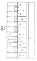
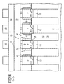
- Figure 2 is a Sectional view along the section line BBn shown in Figure 1.
- the substrate 1 which is an SOI substrate 2, which has an insulation layer 12
- a first selection transistor 16 is arranged in the substrate 1, which is an SOI substrate 2, which has an insulation layer 12.
- the first Selection transistor 16 has a first source doping region 24 and a first word line 9.
- the first word line 9 is surrounded with an insulating word line sleeve 34.
- Farther is the first selection transistor 16 with an n-channel capacitor connection 5 and a first bit line connection 7 connected.
- a second one Word line 10 and a third word line 11 are arranged.
- n-channel region 3 is of Trench isolation 26 included.
- the trench insulation 26 made of silicon oxide
- the active n-channel region 3 made of p-doped silicon
- the first Source doping region 24 made of highly n-doped silicon
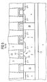
- FIG 3 is a sectional view along the section line BBp shown in Figure 1.
- the structure of that shown in Figure 3 Arrangement is equivalent to that shown in Figure 2 Structure, but some dopings are reversed, since there is an active p-channel region 4 for the p-channel transistors is used.
- the substrate 1 is concerned again an SOI substrate, with a second selection transistor 17 is formed in an active p-channel region 4.
- the second selection transistor 17 is also connected to the first Word line 9 connected, and also has a second, highly n-doped source doping region 25.
- the second source doping region 25 is connected to a p-channel capacitor connection 6 connected.
- the second selection transistor 17 via a second bit line connection 8 connected to the second bit line 23.
- the SOI substrate 2 has an insulation layer 12.
- the active p-channel area 4 is isolated by means of the trench isolation 26. Run above the active p-channel region 4 in this Embodiment the first word line 9 and the second Word line 10.
- the third word line 11 runs
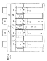
- FIG 6 is a sectional view along the section line AA shown in Figure 1.
- the insulation layer 12 is arranged.
- active n-channel regions 3 and active p-channel regions 4 are arranged, which are isolated from one another by trench insulation 26 become.
- first source doping region 24 via the n-channel capacitor connection 5 with the first capacitor 18, which is designed as a stacked capacitor is connected.
- the trench isolation 26 arranged next to which the active p-channel region 4 is arranged.
- the second is in the active p-channel region 4 Source doping region 25 arranged in the upper region, the over the p-channel capacitor connection 6 with the second storage capacitor 19, which is also designed as a stacked capacitor is connected.
- FIGS. 7 to 11 show a variant with trench capacitors to the memory cell array 13 shown in FIG. 1 described.
- the substrate 1 which as SOI substrate 2 is formed with the insulation layer 12 Mistake.
- the trench capacitors 20 protrude through the insulation layer 12 through.
- a first selection transistor 16 is arranged, which has a first source doping region 24.
- the first source doping region 24 is connected to the first storage capacitor, for example 18, which is designed as a trench capacitor 20, connected.
- the first selection transistor 16 via the first bit line connection 7 to the first bit line 22 connected.
- the first Selection transistor 16 controls, run a second Word line 10 and a third word line 11.
- the second Word line 10 also runs above the active n-channel region 3, the third word line 11 runs above a trench isolation 26.
- an insulation layer 33 which for example consists of a BPSG is formed.
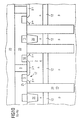
- FIG 8 is a sectional view along the section line BBp shown in Figure 1.
- the arrangement is in the substrate 1 formed, which is an SOI substrate 2.
- the Trench capacitors also extend through the insulation layer 12.
- Above the insulation layer 12 is a active p-channel region 4, in which a second selection transistor 17 is formed.
- the second selection transistor 17 has a second source doping region 25, which is connected to a second Storage capacitor 19 is connected as a trench capacitor 20 is formed.
- the second selection transistor 17 is controlled by means of the first word line 9.
- Farther is the second selection transistor 17 via the second bit line connection 8 connected to the second bit line 23.
- an insulation layer 33 made of BPSG is arranged. Neighbors Memory cells are in this embodiment the trench isolation 26 isolated from each other.
- FIG. 9 shows another sectional view along the section line BBn shown in Figure 1.
- Figure 9 differs of Figure 7 in that the trench isolation 26 does not to the insulation layer 12, but a conductive one Layer 27 between the trench isolation 26 and the isolation layer 12 is arranged. This has the advantage that SOI effects of the selection transistors can be avoided because the Cargo can be transported, which is usually in the would accumulate substrate.
- FIG 11 is a sectional view along the section line AA shown in Figure 1.
- the substrate 1 is again an SOI substrate that an insulation layer 12 having.
- the first storage capacitor 18 and the second Storage capacitor 19 are designed as trench capacitors 20 and extend through the insulation layer 12.
- the individual trench capacitors are located above the insulation layer 12 and the active channel areas 3 surrounding them, 4 isolated from one another by means of trench insulation 26.
- Above the trench capacitors 20 and the isolation trench 26 is an isolation layer 33 arranged from BPSG.
- the first memory cell 14 is connected to a first bit line 22, the second memory cell 15 to a second bit line 23. Furthermore, adjacent memory cells with an active n-channel area are connected to the first bit line 22. Further memory cells with an active p-channel region are connected to the second bit line 23.
- a second word line 10 is arranged next to the first word line 9. Sectional images are shown along the section line DDn, DDp and CC in FIGS. 14 to 16.
- FIG. 13 is an enlarged plan view of the one in FIG 12 shown memory cell array 13 shown.
- the substrate 1 which is formed as an SOI substrate 2
- the active n-channel and p-channel areas on both sides with the period of the smallest structural dimension F.
- the first word line 9 is a spacer word line around the active n-channel region 3 and the active p-channel region 4 are formed.
- the second word line 10 is arranged adjacent to the first word line 9. Lateral are transverse to the course of the first word line 9 Isolation edge webs 35 on the active channel areas 3, 4 formed.
- Figure 14 is a sectional view along the section line DDn shown in Figure 12.
- the substrate 1 12 There is an insulation layer in the substrate 1 12 arranged because the substrate as SOI substrate 2nd is trained.
- Above the insulation layer 12 is a active n-channel region 3, in which the first selection transistor 16 is formed as a vertical transistor.
- the first selection transistor 16 a first source doping region 24 and a first drain doping region 36.
- the first drain doping region 36 is with the first storage capacitor 18 connected, which is designed as a trench capacitor 20.
- the first word line 9 runs next to the active n-channel region 3 and is isolated by a gate oxide. Adjacent to that active n-channel area 3 is another active n-channel area, which is surrounded by the second word line 10.
- the first source doping region 24 is with the first bit line 22 connected. Adjacent word lines are with the Isolation 41 isolated from each other.
- the first bit line 22 is insulated with a bit line insulation sheath 38. Above the bit line insulation sheath 38 is an insulation layer 33 arranged. Run above the insulation layer 33 a first metal word line 39 and a second metal word line 40, with the first word line 9 and the second word line 10 are connected to the trained as a spacer Word lines 9, 10 to make low-resistance.
- the active p-channel area 4 is from the first Word line 9, which also the second selection transistor 17th controls, isolated by a gate oxide. Adjacent to the first Word line 9 runs the second word line 10, the also surrounds an active p-channel area here. Above the second bit line 23 is a bit line insulation jacket 38 arranged on which the insulation layer 33 extends. Above the insulation layer 33 are the first metal word line 39 and the second metal word line 40 arranged with the first word line 9 and the second word line 10 are connected in order to train them with lower resistance.
- the SOI substrate 2 has an insulation layer 12 on, on the alternately active n-channel area 3 and active p-channel region 4 are arranged.
- the active n-channel area 3 and the active p-channel area 4 are insulated from lateral isolation edge webs 35 (spacer).
- the first word line 9 runs next to the active n-channel area 3 and the active p-channel area 4.
- Das first source doping region 24 is on the first bit line 22 and the second source doping region 25 is on the second bit line 23 connected.
- the first bit line 22 and the second bit lines 23 are from a bit line insulation sleeve 38 surrounded.
- Through the Insulation layer 33 is a metallic word line contact 42 provided with which the first metal word line 39 which runs above the insulation layer 33 with the first word line 9 is connected.
- the substrate is usually made of silicon. Also the SOI substrate used in this case consists of silicon, however, has a buried insulation layer 12 in the substrate 1.
- the active n-channel area it is, for example, a weakly p-doped silicon, the active p-channel region is a weakly n-doped silicon.
Landscapes
- Engineering & Computer Science (AREA)
- Manufacturing & Machinery (AREA)
- Semiconductor Memories (AREA)
- Dram (AREA)
- Element Separation (AREA)
Abstract
Description
- eine erste Speicherzelle mit einem ersten Auswahltransistor und einem ersten Speicherkondensator und
- eine zweite Speicherzelle mit einem zweiten Auswahltransistor und einem zweiten Speicherkondensator angeordnet sind,
- wobei der erste Auswahltransistor ein n-Kanal-Transistor und der zweite Auswahltransistor ein p-Kanal-Transistor ist und
- wobei die Speicherzellen in einem SOI-Substrat, das eine Isolationsschicht aufweist, gebildet sind.
- Figur 1
- die Draufsicht auf eine Anordnung von Speicherzellen bestehend aus Auswahltransistoren und Speicherkondensatoren, wobei p- und n-Kanal-Transistoren ausgebildet sind;
- Figur 2
- ein Schnittbild entlang der Schnittlinie BBn aus Figur 1 für Stacked-Kondensatoren;
- Figur 3
- ein Schnittbild entlang der Schnittlinie BBp aus Figur 1 für Stacked-Kondensatoren;
- Figur 4
- ein Schnittbild entlang der Schnittlinie BBn aus Figur 1, wobei das STI (Shallow Trench Isolation) nicht bis zu der Isolationsschicht des SOI-Substrats (Silicon on Insulator) gebildet wurde;
- Figur 5
- ein Schnittbild entlang der Schnittlinie BBp aus Figur 1, ebenfalls mit angehobenem STI;
- Figur 6
- ein Schnittbild entlang der Schnittebene AA aus Figur 1;
- Figur 7
- ein Schnittbild entlang der Schnittlinie BBn aus Figur 1 mit Grabenkondensatoren;
- Figur 8
- ein Schnittbild entlang der Schnittlinie BBp aus Figur 1 mit Grabenkondensatoren;
- Figur 9
- ein Schnittbild entlang der Schnittlinie BBn aus Figur 1 mit Grabenkondensatoren und angehobenem STI;
- Figur 10
- ein Schnittbild entlang der Schnittlinie BBp aus Figur 1 mit Grabenkondensatoren und angehobenem STI;
- Figur 11
- ein Schnittbild entlang der Schnittlinie AA aus Figur 1 mit Grabenkondensatoren;
- Figur 12
- die Draufsicht auf eine Anordnung von Speicherzellen bestehend aus Auswahltransistoren und Speicherkondensatoren, wobei die Auswahltransistoren als n-Kanal-Transistoren und p-Kanal-Transistoren ausgebildet sind;
- Figur 13
- die Draufsicht auf einen aus Figur 12 herausvergrößerten Bereich, bei dem der Verlauf der Wortleitungen herausvergrößert ist;
- Figur 14
- ein Schnittbild entlang der Schnittlinie DDn aus Figur 12 mit Grabenkondensatoren;
- Figur 15
- ein Schnittbild entlang der Schnittlinie DDp aus Figur 12 mit Grabenkondensatoren;
- Figur 16
- Ein Schnittbild entlang der Schnittlinie CC aus Figur 12.
- 1
- Substrat
- 2
- SOI-Substrat
- 3
- Aktives n-Kanalgebiet
- 4
- Aktives p-Kanalgebiet
- 5
- n-Kanal-Kondensatoranschluß
- 6
- p-Kanal-Kondensatoranschluß
- 7
- Erster Bitleitungsanschluß
- 8
- Zweiter Bitleitungsanschluß
- 9
- Erste Wortleitung
- 10
- Zweite Wortleitung
- 11
- Dritte Wortleitung
- 12
- Isolationsschicht
- 13
- Speicherzellenfeld
- 14
- Erste Speicherzelle
- 15
- Zweite Speicherzelle
- 16
- Erster Auswahltransistor
- 17
- Zweiter Auswahltransistor
- 18
- Erster Speicherkondensator
- 19
- Zweiter Speicherkondensator
- 20
- Grabenkondensator
- 21
- Stapelkondensator
- 22
- Erste Bitleitung
- 23
- Zweite Bitleitung
- 24
- erstes Source-Dotiergebiet
- 25
- zweites Source-Dotiergebiet
- 26
- Grabenisolation
- 27
- leitende Schicht
- 28
- Dotierstoff
- 29
- erste Wortleitungsspannung
- 30
- zweite Wortleitungsspannung
- 31
- dritte Wortleitungsspannung
- 32
- Gate-Material
- 33
- Isolationsschicht
- 34
- isolierende Wortleitungshülle
- 35
- Isolationsrandsteg
- 36
- erstes Drain-Dotiergebiet
- 37
- zweites Drain-Dotiergebiet
- 38
- isolierende Bitleitungshülle
- 39
- erste Metallwortleitung
- 40
- zweite Metallwortleitung
- 41
- Isolation
- 42
- Metallwortleitungskontakt
Claims (11)
- Halbleiterspeicher mit einem Speicherzellenfeld (13), in demeine erste Speicherzelle (14) mit einem ersten Auswahltransistor (16) und einem ersten Speicherkondensator (18) undeine zweite Speicherzelle (15) mit einem zweiten Auswahltransistor (17) und einem zweiten Speicherkondensator (19) angeordnet sind,wobei der erste Auswahltransistor (16) ein n-Kanal-Transistor und der zweite Auswahltransistor (17) ein p-Kanal-Transistor ist undwobei die Speicherzellen (14, 15) in einem SOI-Substrat (2), das eine Isolationsschicht (12) aufweist, gebildet sind.
- Halbleiterspeicher nach Anspruch 1,
dadurch gekennzeichnet, daß
mindestens einer der Speicherkondensatoren (18, 19) ein Grabenkondensator (20) ist. - Halbleiterspeicher nach Anspruch 1,
dadurch gekennzeichnet, daß
mindestens einer der Speicherkondensatoren (18, 19) ein Stapelkondensator (21) ist. - Halbleiterspeicher nach einem der Ansprüche 1 bis 3,
dadurch gekennzeichnet, daß
eine Grabenisolation (26) und die Isolationsschicht (12) den ersten Auswahltransistor (16) von dem zweiten Auswahltransistor (17) isolieren. - Halbleiterspeicher nach einem der Ansprüche 1 bis 4,
dadurch gekennzeichnet, daß
der erste Auswahltransistor (16) oder der zweite Auswahltransistor (17) als vertikaler Transistor gebildet sind. - Halbleiterspeicher nach einem der Ansprüche 1 bis 5,
dadurch gekennzeichnet, daß
der erste Auswahltransistor (16) ein Gate aus einem Mid-Gap-Material aufweist, welches so gewählt ist, daß die Einsatzspannung des ersten Auswahltransistors (16) die negative Einsatzspannung des zweiten Auswahltransistors (17) ist. - Halbleiterspeicher nach einem der Ansprüche 1 bis 6,
dadurch gekennzeichnet, daß
als ein Gate-Material für den ersten Auswahltransistor (16) und/oder für den zweiten Auswahltransistor (17) ein mit Dotierstoff dotiertes Polysilizium verwendet wird. - Halbleiterspeicher nach einem der Ansprüche 6 oder 7,
dadurch gekennzeichnet, daß
als Dotierstoff Germanium verwendet wird. - Halbleiterspeicher nach einem der Ansprüche 1 bis 8,
dadurch gekennzeichnet, daß
ein Gate-Material für den ersten Auswahltransistor (16) und/oder für den zweiten Auswahltransistor (17) Titannitrid, Wolfram oder Tantal enthält. - Halbleiterspeicher nach einem der Ansprüche 1 bis 9,
dadurch gekennzeichnet, daß
zur Verbindung des ersten Speicherkondensators (18) mit einem Source-Dotiergebiet (24) des ersten Auswahltransistors (16) und/oder zur Verbindung des zweiten Speicherkondensators (19) mit einem zweiten Source-Dotiergebiet (25) des zweiten Auswahltransistors (17) ein Silizid verwendet wird. - Halbleiterspeicher nach einem der Ansprüche 5 bis 10,
dadurch gekennzeichnet, daß
zwischen der Grabenisolation (26) und einer Isolationsschicht (12) des SOI-Substrats (2) eine leitfähige Schicht (27) angeordnet ist.
Applications Claiming Priority (2)
| Application Number | Priority Date | Filing Date | Title |
|---|---|---|---|
| DE10015278A DE10015278B4 (de) | 2000-03-28 | 2000-03-28 | Halbleiterspeicher mit einem Speicherzellenfeld |
| DE10015278 | 2000-03-28 |
Publications (2)
| Publication Number | Publication Date |
|---|---|
| EP1139425A2 true EP1139425A2 (de) | 2001-10-04 |
| EP1139425A3 EP1139425A3 (de) | 2006-08-16 |
Family
ID=7636622
Family Applications (1)
| Application Number | Title | Priority Date | Filing Date |
|---|---|---|---|
| EP01105818A Withdrawn EP1139425A3 (de) | 2000-03-28 | 2001-03-08 | DRAM-Speicherzellenfeld mit n- und p-Kanal-Transistoren |
Country Status (6)
| Country | Link |
|---|---|
| US (1) | US6469335B2 (de) |
| EP (1) | EP1139425A3 (de) |
| JP (1) | JP3905713B2 (de) |
| KR (1) | KR100382673B1 (de) |
| DE (1) | DE10015278B4 (de) |
| TW (1) | TW499678B (de) |
Families Citing this family (11)
| Publication number | Priority date | Publication date | Assignee | Title |
|---|---|---|---|---|
| DE10134101B4 (de) * | 2001-07-13 | 2006-03-23 | Infineon Technologies Ag | Integrierter Halbleiterspeicher und Herstellungsverfahren |
| US20030048656A1 (en) | 2001-08-28 | 2003-03-13 | Leonard Forbes | Four terminal memory cell, a two-transistor sram cell, a sram array, a computer system, a process for forming a sram cell, a process for turning a sram cell off, a process for writing a sram cell and a process for reading data from a sram cell |
| DE10362018B4 (de) * | 2003-02-14 | 2007-03-08 | Infineon Technologies Ag | Anordnung und Verfahren zur Herstellung von vertikalen Transistorzellen und transistorgesteuerten Speicherzellen |
| DE10340714B3 (de) * | 2003-09-04 | 2005-05-25 | Infineon Technologies Ag | Teststruktur für ein Single-sided Buried Strap-DRAM-Speicherzellenfeld |
| US20060286759A1 (en) * | 2005-06-21 | 2006-12-21 | Texas Instruments, Inc. | Metal oxide semiconductor (MOS) device having both an accumulation and a enhancement mode transistor device on a similar substrate and a method of manufacture therefor |
| JP4267009B2 (ja) * | 2005-09-26 | 2009-05-27 | エルピーダメモリ株式会社 | 半導体メモリおよびその製造方法 |
| US8310859B2 (en) | 2008-09-30 | 2012-11-13 | Samsung Electronics Co., Ltd. | Semiconductor memory device having balancing capacitors |
| US20170221899A1 (en) * | 2016-01-29 | 2017-08-03 | Semiconductor Energy Laboratory Co., Ltd. | Microcontroller System |
| US11670588B2 (en) * | 2019-01-09 | 2023-06-06 | Intel Corporation | Selectable vias for back end of line interconnects |
| US12501624B1 (en) | 2024-09-25 | 2025-12-16 | Globalfoundries U.S. Inc. | Memory device structures that include a capacitor |
| EP4718967A1 (de) * | 2024-09-25 | 2026-04-01 | GlobalFoundries U.S. Inc. | Speichervorrichtungsstrukturen mit einem kondensator |
Family Cites Families (19)
| Publication number | Priority date | Publication date | Assignee | Title |
|---|---|---|---|---|
| JPS5782279A (en) | 1980-11-04 | 1982-05-22 | Fujitsu Ltd | Semiconductor storage device |
| JPS61280651A (ja) * | 1985-05-24 | 1986-12-11 | Fujitsu Ltd | 半導体記憶装置 |
| JPS62202397A (ja) * | 1986-02-28 | 1987-09-07 | Fujitsu Ltd | 半導体記憶装置 |
| US4807195A (en) | 1987-05-18 | 1989-02-21 | International Business Machines Corporation | Apparatus and method for providing a dual sense amplifier with divided bit line isolation |
| US4954854A (en) * | 1989-05-22 | 1990-09-04 | International Business Machines Corporation | Cross-point lightly-doped drain-source trench transistor and fabrication process therefor |
| US5323343A (en) * | 1989-10-26 | 1994-06-21 | Mitsubishi Denki Kabushiki Kaisha | DRAM device comprising a stacked type capacitor and a method of manufacturing thereof |
| JP3241059B2 (ja) * | 1991-03-29 | 2001-12-25 | 株式会社東芝 | ダイナミック型半導体記憶装置 |
| US5494841A (en) * | 1993-10-15 | 1996-02-27 | Micron Semiconductor, Inc. | Split-polysilicon CMOS process for multi-megabit dynamic memories incorporating stacked container capacitor cells |
| JP3315293B2 (ja) * | 1995-01-05 | 2002-08-19 | 株式会社東芝 | 半導体記憶装置 |
| JPH08340088A (ja) * | 1995-06-09 | 1996-12-24 | Toshiba Microelectron Corp | ダイナミック型メモリ |
| US5585285A (en) * | 1995-12-06 | 1996-12-17 | Micron Technology, Inc. | Method of forming dynamic random access memory circuitry using SOI and isolation trenches |
| EP0838858B1 (de) * | 1996-09-27 | 2002-05-15 | Infineon Technologies AG | Integrierte CMOS-Schaltungsanordnung und Verfahren zu deren Herstellung |
| KR100239414B1 (ko) * | 1996-11-07 | 2000-01-15 | 김영환 | 반도체 소자의 제조방법 |
| DE19653107C2 (de) * | 1996-12-19 | 1998-10-08 | Siemens Ag | Verfahren zur Herstellung einer Speicherzellenanordnung |
| US5867420A (en) * | 1997-06-11 | 1999-02-02 | Siemens Aktiengesellschaft | Reducing oxidation stress in the fabrication of devices |
| US5952701A (en) * | 1997-08-18 | 1999-09-14 | National Semiconductor Corporation | Design and fabrication of semiconductor structure having complementary channel-junction insulated-gate field-effect transistors whose gate electrodes have work functions close to mid-gap semiconductor value |
| US6037620A (en) * | 1998-06-08 | 2000-03-14 | International Business Machines Corporation | DRAM cell with transfer device extending along perimeter of trench storage capacitor |
| JP3660821B2 (ja) * | 1999-01-19 | 2005-06-15 | 株式会社日立製作所 | 半導体装置およびその製造方法 |
| US6358820B1 (en) * | 2000-04-17 | 2002-03-19 | Mitsubishi Denki Kabushiki Kaisha | Method of manufacturing semiconductor device |
-
2000
- 2000-03-28 DE DE10015278A patent/DE10015278B4/de not_active Expired - Fee Related
-
2001
- 2001-03-08 EP EP01105818A patent/EP1139425A3/de not_active Withdrawn
- 2001-03-27 TW TW090107180A patent/TW499678B/zh not_active IP Right Cessation
- 2001-03-28 JP JP2001093972A patent/JP3905713B2/ja not_active Expired - Fee Related
- 2001-03-28 US US09/820,234 patent/US6469335B2/en not_active Expired - Lifetime
- 2001-03-28 KR KR10-2001-0016229A patent/KR100382673B1/ko not_active Expired - Fee Related
Also Published As
| Publication number | Publication date |
|---|---|
| US6469335B2 (en) | 2002-10-22 |
| JP2001308298A (ja) | 2001-11-02 |
| US20010032991A1 (en) | 2001-10-25 |
| KR20010093742A (ko) | 2001-10-29 |
| TW499678B (en) | 2002-08-21 |
| DE10015278B4 (de) | 2004-09-23 |
| JP3905713B2 (ja) | 2007-04-18 |
| KR100382673B1 (ko) | 2003-05-09 |
| DE10015278A1 (de) | 2001-10-04 |
| EP1139425A3 (de) | 2006-08-16 |
Similar Documents
| Publication | Publication Date | Title |
|---|---|---|
| EP2169715B1 (de) | Integrierte Schaltungsanordnung mit Kondensator und Herstellungsverfahren | |
| DE4208694C2 (de) | Halbleiter-Speicherelement | |
| DE3689467T2 (de) | Speicher mit hoher Dichte. | |
| DE3844120C2 (de) | Halbleitereinrichtung mit grabenförmiger Struktur | |
| DE3915438C2 (de) | ||
| DE19832795B4 (de) | Statische Zelle eines Speichers für wahlfreien Zugriff mit optimiertem Seitenverhältnis und Halbleiterspeichervorrichtung, die mindestens eine Speicherzelle umfasst | |
| EP0766312B1 (de) | Selbstverstärkende DRAM-Speicherzellenanordnung | |
| DE3203516A1 (de) | Nicht fluechtige, elektrisch umprogrammierbare floating-gate-speicheranordnung | |
| DE10334424A1 (de) | Halbleiterspeichervorrichtung mit Doppelzelleneinheiten | |
| DE3688694T2 (de) | Rillenartiger Kondensator und DRAM-Speicherzelle. | |
| EP1139425A2 (de) | DRAM-Speicherzellenfeld mit n- und p-Kanal-Transistoren | |
| WO2000019529A1 (de) | Integrierte schaltungsanordnung mit vertikaltransistoren und verfahren zu deren herstellung | |
| DE3046524C2 (de) | Halbleitervorrichtung | |
| DE19929211B4 (de) | Verfahren zur Herstellung eines MOS-Transistors sowie einer DRAM-Zellenanordung | |
| EP0917203A2 (de) | Gain Cell DRAM Struktur und Verfahren zu deren Herstellung | |
| EP1160844A2 (de) | Speicherzellenanordnung | |
| DE102004021051B3 (de) | DRAM-Speicherzellenanordnung nebst Betriebsverfahren | |
| DE19950362C1 (de) | DRAM-Zellenanordnung, Verfahren zu deren Betrieb und Verfahren zu deren Herstellung | |
| DE10226583B4 (de) | DRAM-Speicherzelle für schnellen Schreib-/Lesezugriff und Speicherzellenfeld | |
| DE10320874B4 (de) | Integrierter Halbleiterspeicher mit einem Transistor verringerter Gate-Oxiddicke | |
| DE19727436C1 (de) | DRAM-Zellenanordnung mit dynamischen selbstverstärkenden Speicherzellen und Verfahren zu deren Herstellung | |
| DE3643635C2 (de) | ||
| EP1202286B1 (de) | DRAM-Speicherzelle | |
| EP1111682A2 (de) | DRAM-Zelle mit zwei MOS-Transistoren | |
| DE102008001210A1 (de) | SRAM-Bauelement |
Legal Events
| Date | Code | Title | Description |
|---|---|---|---|
| PUAI | Public reference made under article 153(3) epc to a published international application that has entered the european phase |
Free format text: ORIGINAL CODE: 0009012 |
|
| AK | Designated contracting states |
Kind code of ref document: A2 Designated state(s): AT BE CH CY DE DK ES FI FR GB GR IE IT LI LU MC NL PT SE TR |
|
| AX | Request for extension of the european patent |
Free format text: AL;LT;LV;MK;RO;SI |
|
| PUAL | Search report despatched |
Free format text: ORIGINAL CODE: 0009013 |
|
| AK | Designated contracting states |
Kind code of ref document: A3 Designated state(s): AT BE CH CY DE DK ES FI FR GB GR IE IT LI LU MC NL PT SE TR |
|
| AX | Request for extension of the european patent |
Extension state: AL LT LV MK RO SI |
|
| AKX | Designation fees paid | ||
| STAA | Information on the status of an ep patent application or granted ep patent |
Free format text: STATUS: THE APPLICATION IS DEEMED TO BE WITHDRAWN |
|
| 18D | Application deemed to be withdrawn |
Effective date: 20070217 |
|
| REG | Reference to a national code |
Ref country code: DE Ref legal event code: 8566 |