EP1111682A2 - DRAM-Zelle mit zwei MOS-Transistoren - Google Patents
DRAM-Zelle mit zwei MOS-Transistoren Download PDFInfo
- Publication number
- EP1111682A2 EP1111682A2 EP00126788A EP00126788A EP1111682A2 EP 1111682 A2 EP1111682 A2 EP 1111682A2 EP 00126788 A EP00126788 A EP 00126788A EP 00126788 A EP00126788 A EP 00126788A EP 1111682 A2 EP1111682 A2 EP 1111682A2
- Authority
- EP
- European Patent Office
- Prior art keywords
- mosfet
- memory cell
- connection
- memory
- trench
- Prior art date
- Legal status (The legal status is an assumption and is not a legal conclusion. Google has not performed a legal analysis and makes no representation as to the accuracy of the status listed.)
- Withdrawn
Links
Images


Classifications
-
- H—ELECTRICITY
- H10—SEMICONDUCTOR DEVICES; ELECTRIC SOLID-STATE DEVICES NOT OTHERWISE PROVIDED FOR
- H10B—ELECTRONIC MEMORY DEVICES
- H10B12/00—Dynamic random access memory [DRAM] devices
-
- H—ELECTRICITY
- H10—SEMICONDUCTOR DEVICES; ELECTRIC SOLID-STATE DEVICES NOT OTHERWISE PROVIDED FOR
- H10B—ELECTRONIC MEMORY DEVICES
- H10B12/00—Dynamic random access memory [DRAM] devices
- H10B12/01—Manufacture or treatment
-
- H—ELECTRICITY
- H10—SEMICONDUCTOR DEVICES; ELECTRIC SOLID-STATE DEVICES NOT OTHERWISE PROVIDED FOR
- H10B—ELECTRONIC MEMORY DEVICES
- H10B12/00—Dynamic random access memory [DRAM] devices
- H10B12/01—Manufacture or treatment
- H10B12/02—Manufacture or treatment for one transistor one-capacitor [1T-1C] memory cells
- H10B12/05—Making the transistor
- H10B12/053—Making the transistor the transistor being at least partially in a trench in the substrate
Definitions
- the invention relates to an integrated dynamic memory cell with a small spreading area, which in one in the Substrate etched trench is integrated.
- a dynamic semiconductor memory consists of a large number of memory cells.
- a conventional memory cell has one Storage capacity on the via a selection transistor to the Bit line BL can be connected. Becomes a word line WL is set to a high voltage level, the selection transistor opens, and the storage capacity is sent to the bit line BL switched. In this state, a date can be entered into the Memory cell can be written by the capacity on the desired memory content is unloaded or charged.
- a disadvantage of the conventional memory cell is that that with increasing integration to smaller structures the capacity of the storage capacitor cannot be reduced can. Therefore, in EP 0537203 B1 the one in FIG Memory cell shown with two MOSFET transistors proposed. However, the spreading area is the one described there Memory cell relatively large because of the memory cell is formed planar on the substrate surface.
- the invention provides an integrated dynamic memory cell with a small propagation area, which has a selection MOSFET with a gate connection region which is connected to a word line, a source connection doping region which is connected to a bit line and with a drain connection doping region, and a memory MOSFET having a gate connection region which is connected via a thin dielectric layer to a connection doping region which connects a source connection doping region of the memory MOSFET to the drain connection doping region of the selection MOSFET and with a drain connection -Doping range, which is applied to a supply voltage, wherein the selection MOSFET and the memory MOSFET are arranged in a trench etched into the semiconductor substrate on the side walls of the trench such that they lie opposite one another and the connection doping region forms the bottom of the etched trench.
- dynamic memory cell is the select MOSFET and the memory MOSFET one NMOS transistor each.
- Memory cell has the thin dielectric layer a thickness of less than 2 nm so that the thin dielectric layer is permeable to tunnel currents.
- the are through tunnel currents flowing through the thin dielectric layer the doping of the gate connection region and the connection doping region adjustable.
- the thin dielectric layer preferably has an asymmetrical one Current transmission characteristic similar to a diode.
- the thin dielectric layer preferably consists of a Oxide, nitride or oxynitride.
- dynamic memory cell exhibit the selection MOSFET and the memory MOSFET each have a gate oxide layer which run along the side walls of the etched trench.
- dynamic Memory cell are the gate connection areas of the Selection MOSFETs and memory MOSFETs formed by spacers.
- the source connection areas and the drain connection areas of the two MOSFETS and the connection doping region Ion implantation doped.
- dynamic memory cells lie next to the gate oxide layers of the select MOSFET and the memory MOSFET, respectively doped current-conducting channels, the doping of which is used to determine the respective threshold voltage of the two MOSFETS adjustable is.
- the doped current conduction channels are preferably through Ion implantation doped.
- the width of the etched trench corresponds to one in particular preferred embodiment of the dynamic according to the invention Memory cell of the minimum lithographic structure size.
- the length of the doped current-conducting channels preferably corresponds to this essentially the depth of the etched trench.
- the depth of the etched trench is greater than the width of the etched trench.
- the gate terminal area of the selection MOSFET a dynamic memory cell by an in the etched Trench continuous spacer formed, the gate connection area for a variety of other selection MOSFETs from other dynamic memory cells.
- the spread area of the dynamic memory cell is about four times the square lithographic Structure size.
- the semiconductor substrate areas of selection MOSFETS different Storage cells on a sidewall of the etched trench are preferably arranged by insulating layers arranged separately from each other.
- Dynamic memory cells are the semiconductor substrate areas of memory MOSFETs that are on an opposite Side of the etched trench are also arranged separated from each other by insulating layers.
- the inventive method creates a self-reinforcing dynamic memory cell that takes up very little space Has.
- the manufacturing process is special simply because the masks formed are strip-shaped, which makes photolithography is greatly simplified.
- the etched Trench for receiving the MOSFETs relatively into the memory cell deep, the current conducting channels of the MOSFETS are also relative long so that leakage currents flowing through the selection transistor can drain, are particularly low.
- the asymmetrical Passage characteristic due to the tunnel currents through the thin dielectric layer can by doping the adjacent doped layers can be set. Hereby can the dynamic behavior of the memory cell accordingly the desired application.
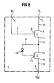
- the integrated dynamic memory cell 1 essentially consists of two MOSFET transistors 2, 3.
- the MOSFET transistors 2, 3 are preferably NMOS MOSFETs.
- the memory cell 1 has a first connection 4 for connection to a word line WL, a second connection 5 for connection to a bit line BL and a third connection 6 for connection to a supply voltage V DD of the memory.
- the word line 4 is connected to the gate 8 of the MOSFET 2 via a line 7.
- the source terminal 9 of the MOSFET 2 is connected to the bit line terminal 5 via a line 10.
- the drain connection 11 of the MOSFET 2 is connected to the source connection 13 of the MOSFET 3 via a connecting line 12.
- the drain connection 14 of the MOSFET 3 is connected to the supply voltage connection 6 via a line 15.
- the gate 15 is coupled to the connecting line 12 of the two MOSFETS 2, 3 via a component 16 shown as a diode and a power line 17.
- the component 16 behaves similarly to a diode or an asymmetrical resistor and has an asymmetrical current transmission characteristic.
- Fig. 8 Memory cell The operation of the invention shown in Fig. 8 Memory cell is as follows.
- a charge can be written into the memory cell 1 and stored become.
- the MOSFET 2 forms the selection MOSFET Memory cell 1
- the MOSFET 3 forms the memory MOSFET the memory cell 1.
- the bit line terminal 5 and the word line terminal 4 both to a logic high voltage level brought.
- the selection MOSFET 2 is controlled by its Gate terminal 8 turned on, and the logic high voltage level is then on the connecting line 12 between the two MOSFETS 2, 3.
- About the diode-like device 16 is the gate 15 of the in a relatively short charging time Memory MOSFETs 3 charged.
- the gate 15 of the memory MOSFET 3 is used to store the registered load and thus the data.
- the diode-like component 16 has an asymmetrical current transmission characteristic.
- the diode-like Component 16 ensures that the charging process slowed discharge of the charge on gate 15 and ensures that the memory transistor 3 when reading a logic "1" opened for a predetermined time is.
- the bit line connection 5 applied to a logic low voltage level and the word line terminal 4 for opening the selection MOSFET 2 brought to a logic high voltage level.
- the selection MOSFET 2 switches through and pulls the connecting line 12 to the low one applied to the bit line connection 5 logical voltage level.
- the gate 15 discharges with a time delay via the diode-like component 16. It flows additionally, as long as there is enough gate charge on the gate 15 of the Memory MOSFETs located a relatively high current from that Supply voltage connection 6 via lines 15, 12, 10 towards the bit line connection 5, since both MOSFETS 2, 3 are switched through.
- the inventive, integrated dynamic memory cell is characterized by the property that the in the memory cell 1 registered charge is less than the charge, which is obtained when reading from memory cell 1.
- the invention dynamic memory cell is therefore self-reinforcing.
- the process according to the invention is also used for the production of the invention shown in Fig. 8 as a circuit diagram integrated dynamic memory cell 1 described.
- a structured one Etching hard mask applied with a TEOS deposition.
- the hard mask consists of a large number of strips, their distance and width about the minimum lithographic Structure size F corresponds.
- the minimal lithographic Structure size F is approximately 0.1 to 0.2 ⁇ m.
- Isolation trenches are made into the dry etching process
- Semiconductor substrate etched the isolation trenches serving to the various dynamic memory cells according to the invention to electrically isolate each other on the semiconductor chip.
- the isolation trenches are made with an insulating material, for example filled with an oxide.
- the isolation trenches are so deep that effective electrical insulation of the Variety of dynamic memory cells is guaranteed.
- the isolation trenches are preferably filled in with oxide a CVD process. The surface is then planarized.
- an n-ion implantation takes place for doping the surface of the semiconductor substrate.
- the ions are accelerated in such a way that they reach up to penetrate a certain depth of the semiconductor substrate.
- An n-polysilicon layer is deposited during the ion implantation and structured using a photoresist masking etched in such a way that polysilicon strips perpendicular to the inserted trenches filled with oxide.
- the distance and the width of the polysilicon strips correspond preferably also the minimal lithographic Structure size F.
- the entire structure is then with a structured silicon nitride hard mask for trench etching overdrawn. In a dry etching process, the silicon substrate and the stripes running parallel in it, with Isolation trenches filled with oxide to form a receiving trench for the dynamic MOSFET transistors to be trained Etched memory cell.
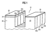
- Fig. 1 you can see a structure that after execution of the process steps mentioned arises.
- a nitride hard mask 20 in which A deep receiving trench 21 is etched in the semiconductor substrate.
- a layer 24 made of n-doped polysilicon.
- areas 22a, 23a alternate pure silicon substrate and regions 22b, 23b made of insulating Oxide.
- n-ions are implanted at the bottom of the etched trench 21 for doping the semiconductor substrate.
- the etching trench 21 is then filled with silicon dioxide in a TEOS process and, after planarization, for example by a chemical-mechanical CMP process, the silicon dioxide filled in the etching trench 21 is etched back in such a way that an insulating oxide layer remains on the trench bottom.
- the etching back takes place selectively in a dry etching process in such a way that the silicon nitride of the hard mask 20 is not attacked.
- the threshold voltage of the later MOSFETS is set by the strength of the doping.
- the implantation of the two opposite side walls of the etching trench 21 can be different, so that the threshold voltage of the two MOSFETS 2, 3 of the memory cell 1 can be set differently.
- the two opposite side walls of the etched trench are thermally oxidized, so that a dielectric oxide layer is formed there.
- This dielectric oxide layer later forms the gate oxide layer for the MOSFETS 2, 3.
- n + polysilicon spacers are formed by polysilicon deposition of polysilicon in the etching trench 21 and subsequent strictly anisotropic etching back of the deposited polysilicon. These polysilicon spacers are then used as a mask for structuring the insulating oxide layer lying on the trench bottom.
- the insulating oxide layer on the trench bottom is selectively etched, so that the structure shown in FIG. 2 is produced.
- FIG. 2 is a sectional view through a silicon semiconductor substrate region 22 after performing the above Process steps. You can see the nitride hard mask layer 20, under which on the left web 22 the Layer 24 of n-polysilicon is located. Then follow on both Pages layers 25, 26 by the n-ion implantation have arisen.
- the structured insulating oxide layer On the bottom of the etched Trench 21 lies over the n-doped region 27, the structured insulating oxide layer.
- the structured isolating Oxide layer consists of two parallel to the side walls 28, 29 extending oxide strips 30, 31. The center of the bottom of the etched trench 21, as can be seen from FIG. 2, free. The two are over the two oxide strips 30, 31 Spacers 32, 33 made of n-polysilicon.
- On the side walls 28, 29 of the etched trench 21 are gate oxide layers.
- the etched trench 21 is now in with silicon dioxide filled in a TEOS process and in such a photo process structured that only half the trench filled with silicon dioxide remains.
- the thin dielectric The layer preferably consists of an NO compound.
- the left one shown in FIG. 2 becomes Spacer 32 is also covered with the oxide nitride compound.
- Fig. 3 arises. You can tell Fig. 3 that the right side of the etched trench 21 for Half is filled with an insulating material 34.
- the Insulating material 34 consists, for example, of silicon dioxide.
- the thin dielectric layer 35 which is preferably made of a Nitrogen-oxygen connection exists. Furthermore, the left one Spacer 32 with a layer 36 of a nitrogen-oxygen compound overdrawn. The left side of the in Fig. 3rd etched trench 21 is then made with n-polysilicon filled and etched this polysilicon back so far that a poly plug 37 remains, as can be seen in FIG. 4 can recognize.
- the thin is made by wet chemical etching Layer 36, which consists of a nitrogen-oxygen compound, removed on the exposed spacer 32, and by a further deposition of polysilicon with subsequent
- the spacer 31 is etched back via a layer 38 made of n-polysilicon connected to the polysilicon plug 37. After one the spacer 32 and the Plug 37, 38 structured such that they are only in the silicon substrate areas 25 stand still and in areas 26, which consist of insulating oxide are removed.
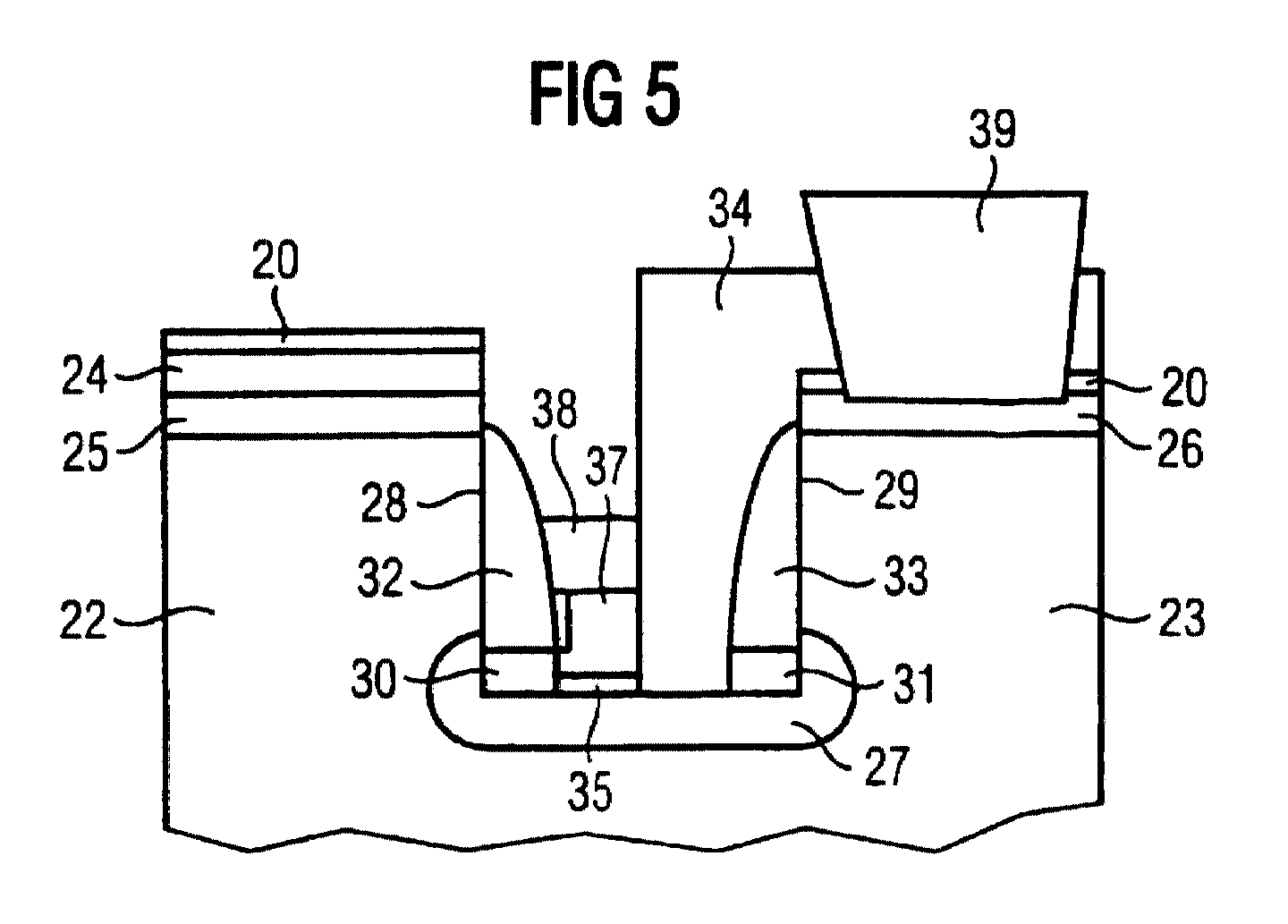
- FIG. 5 shows a first embodiment of the integrated dynamic memory cell 1 according to the invention, which is produced in accordance with the manufacturing method described above.
- the two MOSFETs 2, 3 face the memory cell 1 in the trench 21.
- the MOSFET on the left in FIG. 5 forms the memory MOSFET 3 and the MOSFET on the right forms the selection MOSFET 2.
- the gate 8 of the selection transistor 2 is formed by the spacer 33 is formed, and the gate 15 of the memory transistor 3 is formed by the spacer 32.
- the n-doped layer 25 represents the drain connection of the memory MOSFET 3 and is connected to the supply voltage V DD of the memory.
- the n-doped region 26 forms the source connection region of the selection transistor 2, the metal contact 39 forming the bit line connection 5.
- the drain doping region of the selection transistor 2 on the right and the source doping region of the storage transistor 3 on the left are connected to one another via the connection doping region 27 at the bottom of the etching trench 21.
- the doping region 27 at the bottom of the etched trench 21 forms the conductive connection 12 between the drain terminal 11 of the selection transistor 2 and the source terminal 13 of the memory transistor 3.
- the diode-like component 16 in Fig. 8 is by the thin dielectric layer 35 is formed.
- the thin dielectric Layer 35 consists of an oxide, nitride or a Oxynitride.
- the selection MOSFET 2 on the right side of the etched Trench 21 has a gate connection area that is connected to a word line WL.
- the selection MOSFET 2 also has a source terminal doping region 26, which is connected to a bit line BL via the metal contact 39 is.
- the memory MOSFET 3 has a gate connection region 32 which is connected to the connection doping region 27 via the thin dielectric layer 35.
- the connection doping region 27 connects a source terminal doping region of the memory MOSFET 3 on the left side of the etched trench 21 to the drain terminal doping region of the selection MOSFET 2 on the right side of the etched trench 21.
- the drain terminal doping region 14 of the memory MOSFETs 3 is supplied with the supply voltage V DD of the memory.
- the selection MOSFET 2 and the memory MOSFET 3 are arranged in the trench 21 etched into the semiconductor substrate on the side walls 28, 29 in such a way that they lie opposite one another, the connection doping region 27 forming the bottom of the etched trench 21.
- FIG. 5 shows two NMOS MOSFETs. However, in an alternative embodiment also PMOS-MOSFETS through the manufacturing method according to the invention getting produced.
- the thin dielectric layer 35 is so thin that that through it tunnel currents between the gate connection area 32 of the memory MOSFET 3 and the connection doping region 27 can flow.
- The can by thin dielectric layer 35 flowing tunnel currents the doping of the n-polysilicon region 37 and by the doping of the connection doping region 27 can be set.
- the thin dielectric layer preferably has a thickness of less than 2 nm.
- the etched trench 21 can be etched to any depth become.
- the width of the etched trench 21 preferably corresponds the minimum lithographic structure size F. Since the Length of the doped current-conducting channels that are parallel to the Side walls 28, 29 of the etched trench 21 run through the etching depth of the trench 21 can be set Leakage currents from the memory cell 1 via the selection transistor 2 will flow via the bit line connection 5 by the length of the doped current-conducting channels is increased.
- the gate terminal areas 33 of the one on the right Selection MOSFETs 2, which form the gate 8, run through the etched trench 21.
- the gate connection area the selection MOSFET 2 of the dynamic memory cell 1 is by a continuous in the etched trench 21 Spacer 33 made of n-polysilicon, the same time the gate connection areas for a large number of further selection MOSFETs forms for further dynamic memory cells 1.
- the memory cell 1 according to the invention has a side length that is twice as large as the minimum lithographic structure size F. Accordingly, the spread area of the dynamic memory cell 1 according to the invention is approximately four times the square lithographic structure size 4F 2 .
- the manufacturing method according to the invention for the dynamic Memory cell can be varied. For example, for any leakage currents at the PN junctions on the trench floor to minimize, instead of an n-ion implantation in the trench floor also the doping from a phosphor or arsenic glass layer drive out on the trench floor.
- the memory cell according to the invention becomes the n-polysilicon layer 24 for connection to the supply voltage runs very thick to a larger one Overlap capacity between the supply voltage connection and the gate terminal area 32 of the memory MOSFET 3.
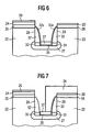
- Manufacturing process can be the process after structuring the spacers 32, 33 made of polysilicon and the Change the insulating oxide layer on the trench floor.
- a thin spacer made of silicon dioxide is placed over the spacers 32a, 33a made of polysilicon.
- the thin dielectric layer 35 becomes thermally at the trench bottom grew up and through deposition and etching back overlying polysilicon plug 37 generated.
- the one so formed Structure can be seen in Fig. 6.
- the structure is then filled with silicon dioxide. Subsequently there is a dry structuring after a Photo process by etching, in which only the memory MOSFET 3 remains exposed. The dry etching also eliminates this the spacers formed from silicon dioxide. A separated afterwards and structured n-polysilicon spacer connects then the polysilicon plug with the gate connection area of the Memory MOSFETs, as can be seen in FIG. 7.
- the gate terminal spacers of the memory MOSFET 3 and the plug are then structured by means of etching in such a way that they only the trench walls formed from silicon semiconductor substrate stop, but on the insulating oxide Trench walls can be removed. The whole structure will then again covered with an intermediate oxide layer and a metallization performed.
Landscapes
- Engineering & Computer Science (AREA)
- Manufacturing & Machinery (AREA)
- Semiconductor Memories (AREA)
- Non-Volatile Memory (AREA)
Abstract
Description
und einen Speicher-MOSFET aufweist mit einem Gateanschluss-Bereich, der über eine dünne dielektrische Schicht an ein Verbindungs-Dotierungsgebiet angeschlossen ist, welches einen Sourceanschluss-Dotierungsbereich des Speicher-MOSFETs mit dem Drainanschluss-Dotierungsbereich des Auswahl-MOSFETs verbindet, und mit einem Drainanschluss-Dotierungsbereich, der an eine Versorgungsspannung anliegt,
wobei der Auswahl-MOSFET und der Speicher-MOSFET in einem in das Halbleitersubstrat geätzten Graben an den Seitenwänden des Grabens derart angeordnet sind, dass sie einander gegenüberliegen und das Verbindungs-Dotierungsgebiet den Boden des geätzten Grabens bildet.
- Fig. 1-5
- mehrere Herstellungsschritte zur Herstellung der erfindungsgemäß integrierten dynamischen Speicherzelle;
- Fig. 6, 7
- die Herstellungsschritte für eine alternative Ausführungsform der erfindungsgemäßen dynamischen Speicherzelle;
- Fig. 8
- ein Schaltkreisdiagramm der erfindungsgemäßen integrierten dynamischen Speicherzelle.
- 1
- Speicherzelle
- 2
- Auswahl-MOSFET
- 3
- Speicher-MOSFET
- 4
- Wortleitungsanschluss
- 5
- Bitleitungsanschluss
- 6
- Versorgungsspannungsanschluss
- 7
- Leitung
- 8
- Gateanschluss
- 9
- Sourceanschluss
- 10
- Leitung
- 11
- Drainanschluss
- 12
- Leitung
- 13
- Sourceanschluss
- 14
- Drainanschluss
- 15
- Gateanschluss
- 16
- diodenähnliches Bauelement
- 17
- Leitung
- 18
- -
- 19
- -
- 20
- Nitrid-Hartmaskenschicht
- 21
- Ätzgraben
- 22
- Halbleitersubstratsteg
- 23
- Halbleitersubstratsteg
- 24
- Polysiliziumschicht
- 25
- Implantationsschicht
- 26
- Implantationsschicht
- 27
- Verbindungs-Dotierungsgebiet
- 28
- Seitenwand des Ätzgrabens
- 29
- Seitenwand des Ätzgrabens
- 30
- Isolierschicht
- 31
- Isolierschicht
- 32
- Spacer
- 33
- Spacer
- 34
- Isoliermaterial
- 35
- dünne dielektrische Schicht
- 36
- dielektrische Abscheidungsschicht
- 37
- Polysiliziumschicht
- 38
- Polysiliziumschicht
- 39
- Metallkontakt
Claims (17)
- Integrierte dynamische Speicherzelle (1) mit geringer Ausbreitungsfläche auf einem Halbleitersubstrat, die aufweist:dadurch gekennzeichnet,(a) einen Auswahl-MOSFET (2) mit einem Gateanschluss-Bereich (8, 33), der mit einer Wortleitung WL verbunden ist, einem Sourceanschluss-Dotierungsbereich (9, 26), der mit einer Bitleitung BL verbunden ist, und mit einem Drainanschluss-Dotierungsbereich (11, 27) ; und(b) einen Speicher-MOSFET (3) mit einem Gateanschluss-Bereich (15, 32), der über eine dünne dielektrische Schicht (35) an ein Verbindungs-Dotierungsgebiet (12, 27) angeschlossen ist, welches einen Sourceanschluss-Dotierungsbereich (13) des Speicher-MOSFETs (3) mit dem Drainanschluss-Dotierungsbereich (11) des Auswahl-MOSFETs (2) verbindet, und mit einem Drainanschluss-Dotierungsbereich (14, 24), der an eine Versorgungsspannung VDD anliegt;(c) wobei der Auswahl-MOSFET (2) und der Speicher-MOSFET (3) in einem in das Halbleitersubstrat geätzten Graben (21) an den Seitenwänden (28, 29) des Grabens (21) derart angeordnet sind, dass sie einander gegenüberliegen und das Verbindungs-Dotierungsgebiet (27) den Boden des geätzten Grabens (21) bildet,
dass die dünne dielektrische Schicht (35) eine Dicke von weniger als 2 nm aufweist, so dass Tunnelströme zwischen dem Gateanschluss-Bereich (32) des Speicher-MOSFETs (3) und dem Verbindungs-Dotierungsgebiet (27) fließen, und dass die durch die dünne dielektrische Schicht (35) fließenden Tunnelströme durch die Dotierung eines aus n-Polysilizium gebildeten Anschlussbereichs (37) und durch die Dotierung des Verbindungs-Dotierungsgebietes (27) einstellbar sind. - Speicherzelle nach Anspruch 1
dadurch gekennzeichnet,
dass der Auswahl-MOSFET (2) und der Speicher-MOSFET (3) NMOS-Transistoren sind. - Speicherzelle nach Anspruch 1 oder 2,
dadurch gekennzeichnet,
dass die dünne dielektrische Schicht (35) eine asymmetrische Stromdurchlasskennlinie aufweist. - Speicherzelle nach einem der vorangehenden Ansprüche,
dadurch gekennzeichnet,
dass die dünne dielektrische Schicht (35) aus Oxid, Nitrid oder einem Oxynitrid besteht. - Speicherzelle nach einem der vorangehenden Ansprüche,
dadurch gekennzeichnet,
dass der Auswahl-MOSFET (2) und der Speicher-MOSFET (3) jeweils eine Gate-oxidschicht aufweisen, die entlang den Seitenwänden (28, 29) des geätzten Grabens (21) verläuft. - Speicherzelle nach einem der vorangehenden Ansprüche,
dadurch gekennzeichnet,
dass die Gateanschluss-Bereiche (32, 33) des Auswahl-MOSFETs (2) und des Speicher-MOSFETs (3) durch Spacer gebildet werden. - Speicherzelle nach einem der vorangehenden Ansprüche,
dadurch gekennzeichnet,
dass die Sourceanschluss-Bereiche und die Drainanschluss-Bereiche und das Verbindungs-Dotierungsgebiet durch Ionenimplantation hergestellt sind. - Speicherzelle nach einem der vorangehenden Ansprüche,
dadurch gekennzeichnet,
dass neben den Gateoxidschichten des Auswahl-MOSFETs (2) und des Speicher-MOSFETs (3) jeweils dotierte Stromleitkanäle liegen, deren Dotierung zur Festlegung der jeweiligen Einsatzspannung der MOSFETs (2, 3) einstellbar ist. - Speicherzelle nach einem der vorangehenden Ansprüche,
dadurch gekennzeichnet,
dass die dotierten Stromleitkanäle durch Ionenimplanatation hergestellt sind. - Speicherzelle nach einem der vorangehenden Ansprüche,
dadurch gekennzeichnet,
dass die Breite des geätzten Grabens (21) der minimalen lithographischen Struktur F entspricht. - Speicherzelle nach einem der vorangehenden Ansprüche,
dadurch gekennzeichnet,
dass die Länge der dotierten Stromleitkanäle im wesentlichen der Tiefe des geätzten Grabens (21) entspricht. - Speicherzelle nach einem der vorangehenden Ansprüche,
dadurch gekennzeichnet,
dass die Tiefe des geätzten Grabens (21) größer ist als dessen Breite. - Speicherzelle nach einem der vorangehenden Ansprüche,
dadurch gekennzeichnet,
dass der Gateanschluss-Bereich (33) des Auswahl-MOSFETs (2) einer dynamischen Speicherzelle (1) durch einen im geätzten Graben durchgängig verlaufenden Spacer (33) gebildet wird, der die Gateanschluss-Bereiche für eine Vielzahl von weiteren Auswahl-MOSFETs von weiteren dynamischen Speicherzellen bildet. - Speicherzelle nach einem der vorangehenden Ansprüche,
dadurch gekennzeichnet,
dass die Ausbreitungsfläche der dynamischen Speicherzelle (1) etwa das Vierfache der quadratischen kleinsten lithographischen Strukturgröße F2 beträgt. - Speicherzelle nach einem der vorangehenden Ansprüche,
dadurch gekennzeichnet,
dass die Halbleitersubstratbereiche von Auswahl-MOSFETs (2) verschiedener Speicherzellen, die auf einer Seitenwand (29) des geätzten Grabens (21) angeordnet sind, durch Isolierschichten voneinander getrennt sind. - Speicherzelle nach einem der vorangehenden Ansprüche,
dadurch gekennzeichnet,
dass die Halbleitersubstratbereiche von Speicher-MOSFETs (3), die auf einer gegenüberliegenden Seite (28) des geätzten Grabens (21) angeordnet sind, durch Isolierschichten voneiannder getrennt sind. - Verfahren zur Herstellung einer integrierten dynamischen Speicherzelle, umfassend die folgenden Schritte:(a) Implantieren der Oberfläche eines Halbleitersubstrats;(b) Ätzen eines Grabens (21) in das Halbleitersubstrat;(c) Implantieren des Halbleitersubstrats am Boden des geätzten Grabens (21) zur Bildung eines Drainanschluss-Dotierungsbereichs (27) und eines Verbindungs-Dotierungsgebietes (27);(d) thermisches Oxidieren der beiden Seitenwände (28, 29) des geätzten Grabens (21) zur Ausbildung von dielektrischen Schichten an den Seitenwänden als Gateisolierschichten für einen Auswahl-MOSFET (2) und einen Speicher-MOSFET (3);(e) Abscheiden einer isolierenden Oxidschicht auf dem Boden des geätzten Grabens;(f) Ausbilden von Polysilizium-Spacern (32, 33) an den Seitenwänden (28, 29) des geätzten Grabens (21) als Gate-Elektroden für den Auswahl-MOSFET (2) und den Speicher-MOSFET (3);(g) Ätzen der isolierenden Oxidschicht mit den gebildeten Polysilizium-Spacern (32, 33) als Maskierung, wobei ein mittlerer Oberflächenbereich des implantierten Substrats beigelegt wird;(h) Füllen einer rechten oder linken Hälfte des geätzten Grabens (21) mit einem isolierenden Material (34);(i) Abscheiden einer von Tunnelströmen durchdringbaren dünnen dielektrischen Schicht (35) auf der verbliebenen freiliegenden Hälfte des mittleren Oberflächenbereichs des Halbleitersubstrats am Boden des geätzten Grabens; und(j) Abscheiden einer Polysiliziumschicht (37, 38) auf der dünnen dielektrischen Schicht (35).
Applications Claiming Priority (2)
| Application Number | Priority Date | Filing Date | Title |
|---|---|---|---|
| DE19961779 | 1999-12-21 | ||
| DE19961779A DE19961779A1 (de) | 1999-12-21 | 1999-12-21 | Integrierte dynamische Speicherzelle mit geringer Ausbreitungsfläche und Verfahren zu deren Herstellung |
Publications (2)
| Publication Number | Publication Date |
|---|---|
| EP1111682A2 true EP1111682A2 (de) | 2001-06-27 |
| EP1111682A3 EP1111682A3 (de) | 2005-09-07 |
Family
ID=7933652
Family Applications (1)
| Application Number | Title | Priority Date | Filing Date |
|---|---|---|---|
| EP00126788A Withdrawn EP1111682A3 (de) | 1999-12-21 | 2000-12-06 | DRAM-Zelle mit zwei MOS-Transistoren |
Country Status (6)
| Country | Link |
|---|---|
| US (1) | US6534820B2 (de) |
| EP (1) | EP1111682A3 (de) |
| JP (1) | JP2001217324A (de) |
| KR (1) | KR100747276B1 (de) |
| DE (1) | DE19961779A1 (de) |
| TW (1) | TW490846B (de) |
Cited By (3)
| Publication number | Priority date | Publication date | Assignee | Title |
|---|---|---|---|---|
| US6396345B2 (en) * | 1999-12-21 | 2002-05-28 | Nortel Networks Limited | Phase and amplitude detector and method of determining errors |
| US9026578B2 (en) | 2004-05-14 | 2015-05-05 | Microsoft Corporation | Systems and methods for persisting data between web pages |
| CN119317098A (zh) * | 2023-07-06 | 2025-01-14 | 长鑫存储技术有限公司 | 半导体结构及其制备方法 |
Families Citing this family (3)
| Publication number | Priority date | Publication date | Assignee | Title |
|---|---|---|---|---|
| KR100487523B1 (ko) * | 2002-04-15 | 2005-05-03 | 삼성전자주식회사 | 부유트랩형 비휘발성 메모리 소자 및 그 제조방법 |
| US6660588B1 (en) | 2002-09-16 | 2003-12-09 | Advanced Micro Devices, Inc. | High density floating gate flash memory and fabrication processes therefor |
| KR100966987B1 (ko) * | 2007-05-07 | 2010-06-30 | 주식회사 하이닉스반도체 | 비휘발성 메모리 소자 및 그의 제조 방법 |
Family Cites Families (9)
| Publication number | Priority date | Publication date | Assignee | Title |
|---|---|---|---|---|
| US4704368A (en) * | 1985-10-30 | 1987-11-03 | International Business Machines Corporation | Method of making trench-incorporated monolithic semiconductor capacitor and high density dynamic memory cells including the capacitor |
| TW199237B (de) * | 1990-07-03 | 1993-02-01 | Siemens Ag | |
| JPH07193140A (ja) * | 1993-12-27 | 1995-07-28 | Toshiba Corp | 半導体記憶装置 |
| ATE212149T1 (de) * | 1995-09-26 | 2002-02-15 | Infineon Technologies Ag | Selbstverstärkende dram-speicherzellenanordnung |
| DE19723936A1 (de) * | 1997-06-06 | 1998-12-10 | Siemens Ag | DRAM-Zellenanordnung und Verfahren zu deren Herstellung |
| DE19727436C1 (de) * | 1997-06-27 | 1998-10-01 | Siemens Ag | DRAM-Zellenanordnung mit dynamischen selbstverstärkenden Speicherzellen und Verfahren zu deren Herstellung |
| DE19727466C2 (de) * | 1997-06-27 | 2001-12-20 | Infineon Technologies Ag | DRAM-Zellenanordnung und Verfahren zu deren Herstellung |
| EP0917203A3 (de) * | 1997-11-14 | 2003-02-05 | Infineon Technologies AG | Gain Cell DRAM Struktur und Verfahren zu deren Herstellung |
| DE19800340A1 (de) * | 1998-01-07 | 1999-07-15 | Siemens Ag | Halbleiterspeicheranordnung und Verfahren zu deren Herstellung |
-
1999
- 1999-12-21 DE DE19961779A patent/DE19961779A1/de not_active Ceased
-
2000
- 2000-12-06 EP EP00126788A patent/EP1111682A3/de not_active Withdrawn
- 2000-12-18 TW TW089127069A patent/TW490846B/zh not_active IP Right Cessation
- 2000-12-19 KR KR1020000078299A patent/KR100747276B1/ko not_active Expired - Fee Related
- 2000-12-21 JP JP2000389217A patent/JP2001217324A/ja not_active Withdrawn
- 2000-12-21 US US09/745,565 patent/US6534820B2/en not_active Expired - Fee Related
Cited By (4)
| Publication number | Priority date | Publication date | Assignee | Title |
|---|---|---|---|---|
| US6396345B2 (en) * | 1999-12-21 | 2002-05-28 | Nortel Networks Limited | Phase and amplitude detector and method of determining errors |
| US9026578B2 (en) | 2004-05-14 | 2015-05-05 | Microsoft Corporation | Systems and methods for persisting data between web pages |
| CN119317098A (zh) * | 2023-07-06 | 2025-01-14 | 长鑫存储技术有限公司 | 半导体结构及其制备方法 |
| CN119317098B (zh) * | 2023-07-06 | 2025-10-21 | 长鑫存储技术有限公司 | 半导体结构及其制备方法 |
Also Published As
| Publication number | Publication date |
|---|---|
| KR100747276B1 (ko) | 2007-08-07 |
| US6534820B2 (en) | 2003-03-18 |
| TW490846B (en) | 2002-06-11 |
| DE19961779A1 (de) | 2001-07-05 |
| JP2001217324A (ja) | 2001-08-10 |
| US20010017795A1 (en) | 2001-08-30 |
| KR20010067426A (ko) | 2001-07-12 |
| EP1111682A3 (de) | 2005-09-07 |
Similar Documents
| Publication | Publication Date | Title |
|---|---|---|
| DE60122656T2 (de) | DRAM Speicherzelle mit Grabenkondensator und vertikalem Transistor | |
| DE19930748C2 (de) | Verfahren zur Herstellung von EEPROM- und DRAM-Grabenspeicherzellbereichen auf einem Chip | |
| DE10320239B4 (de) | DRAM-Speicherzelle und Verfahren zum Herstellen einer solchen DRAM-Speicherzelle | |
| DE3882557T2 (de) | DRAM-Zelle und Herstellungsverfahren. | |
| DE69523091T2 (de) | DRAM-Bauteil mit oberem und unterem Kondensator und Herstellungsverfahren | |
| DE19808182C1 (de) | Elektrisch programmierbare Speicherzellenanordnung und ein Verfahren zu deren Herstellung | |
| DE4443968A1 (de) | Halbleitereinrichtung und Verfahren zum Herstellen derselben | |
| WO2004038770A2 (de) | Integrierte schaltungsanordnung mit kondensator und herstellungsverfahren | |
| EP1179849A2 (de) | Speicherzelle und Herstellungsverfahren | |
| DE3525418A1 (de) | Halbleiterspeichereinrichtung und verfahren zu ihrer herstellung | |
| DE10153765A1 (de) | Verfahren zur Herstellung einer Dram-Zelle mit einem tiefen Graben | |
| EP1399972A2 (de) | Speicherzelle, speicherzellenanordnung und herstellungsverfahren | |
| DE10228096A1 (de) | Speicherzellenlayout mit Doppelgate-Vertikalarray-Transistor | |
| DE4332074A1 (de) | Halbleiterspeichereinrichtung und Verfahren zu ihrer Herstellung | |
| DE19941148A1 (de) | Speicher mit Grabenkondensator und Auswahltransistor und Verfahren zu seiner Herstellung | |
| DE3787687T2 (de) | Halbleiterspeicher. | |
| EP0971414A1 (de) | Grabenkondensator mit Isolationskragen und vergrabenen Kontakt und entsprechendes Herstellungsverfahren | |
| DE19929211B4 (de) | Verfahren zur Herstellung eines MOS-Transistors sowie einer DRAM-Zellenanordung | |
| EP1116270A1 (de) | Integrierte schaltungsanordnung mit vertikaltransistoren und verfahren zu deren herstellung | |
| EP1125328B1 (de) | Verfahren zur herstellung einer dram-zellenanordnung | |
| DE19832095C1 (de) | Stapelkondensator-Herstellungsverfahren | |
| DE10022696A1 (de) | Herstellungsverfahren einer Halbleitereinrichtung und Halbleitereinrichtung | |
| DE10248723A1 (de) | Integrierte Schaltungsanordnung mit Kondensatoren und mit vorzugsweise planaren Transistoren und Herstellungsverfahren | |
| DE10128193C1 (de) | Ein-Transistor-Speicherzellenanordnung und Verfahren zu deren Herstellung | |
| DE102005036561B3 (de) | Verfahren zur Herstellung einer Verbindungsstruktur |
Legal Events
| Date | Code | Title | Description |
|---|---|---|---|
| PUAI | Public reference made under article 153(3) epc to a published international application that has entered the european phase |
Free format text: ORIGINAL CODE: 0009012 |
|
| AK | Designated contracting states |
Kind code of ref document: A2 Designated state(s): AT BE CH CY DE DK ES FI FR GB GR IE IT LI LU MC NL PT SE TR |
|
| AX | Request for extension of the european patent |
Free format text: AL;LT;LV;MK;RO;SI |
|
| PUAL | Search report despatched |
Free format text: ORIGINAL CODE: 0009013 |
|
| AK | Designated contracting states |
Kind code of ref document: A3 Designated state(s): AT BE CH CY DE DK ES FI FR GB GR IE IT LI LU MC NL PT SE TR |
|
| AX | Request for extension of the european patent |
Extension state: AL LT LV MK RO SI |
|
| 17P | Request for examination filed |
Effective date: 20060210 |
|
| AKX | Designation fees paid |
Designated state(s): DE GB |
|
| STAA | Information on the status of an ep patent application or granted ep patent |
Free format text: STATUS: THE APPLICATION IS DEEMED TO BE WITHDRAWN |
|
| 18D | Application deemed to be withdrawn |
Effective date: 20090701 |