EP1139411A1 - Flip-chip Halbleiter-Anordnung mit Rückseiten-Kontaktierung - Google Patents
Flip-chip Halbleiter-Anordnung mit Rückseiten-Kontaktierung Download PDFInfo
- Publication number
- EP1139411A1 EP1139411A1 EP20000106731 EP00106731A EP1139411A1 EP 1139411 A1 EP1139411 A1 EP 1139411A1 EP 20000106731 EP20000106731 EP 20000106731 EP 00106731 A EP00106731 A EP 00106731A EP 1139411 A1 EP1139411 A1 EP 1139411A1
- Authority
- EP
- European Patent Office
- Prior art keywords
- substrate
- semiconductor chip
- connection contacts
- arrangement
- chip
- Prior art date
- Legal status (The legal status is an assumption and is not a legal conclusion. Google has not performed a legal analysis and makes no representation as to the accuracy of the status listed.)
- Withdrawn
Links
Images
Classifications
-
- H—ELECTRICITY
- H10—SEMICONDUCTOR DEVICES; ELECTRIC SOLID-STATE DEVICES NOT OTHERWISE PROVIDED FOR
- H10W—GENERIC PACKAGES, INTERCONNECTIONS, CONNECTORS OR OTHER CONSTRUCTIONAL DETAILS OF DEVICES COVERED BY CLASS H10
- H10W74/00—Encapsulations, e.g. protective coatings
- H10W74/10—Encapsulations, e.g. protective coatings characterised by their shape or disposition
- H10W74/111—Encapsulations, e.g. protective coatings characterised by their shape or disposition the semiconductor body being completely enclosed
- H10W74/114—Encapsulations, e.g. protective coatings characterised by their shape or disposition the semiconductor body being completely enclosed by a substrate and the encapsulations
-
- H—ELECTRICITY
- H10—SEMICONDUCTOR DEVICES; ELECTRIC SOLID-STATE DEVICES NOT OTHERWISE PROVIDED FOR
- H10W—GENERIC PACKAGES, INTERCONNECTIONS, CONNECTORS OR OTHER CONSTRUCTIONAL DETAILS OF DEVICES COVERED BY CLASS H10
- H10W90/00—Package configurations
-
- H—ELECTRICITY
- H10—SEMICONDUCTOR DEVICES; ELECTRIC SOLID-STATE DEVICES NOT OTHERWISE PROVIDED FOR
- H10W—GENERIC PACKAGES, INTERCONNECTIONS, CONNECTORS OR OTHER CONSTRUCTIONAL DETAILS OF DEVICES COVERED BY CLASS H10
- H10W72/00—Interconnections or connectors in packages
- H10W72/071—Connecting or disconnecting
- H10W72/072—Connecting or disconnecting of bump connectors
- H10W72/07231—Techniques
- H10W72/07236—Soldering or alloying
-
- H—ELECTRICITY
- H10—SEMICONDUCTOR DEVICES; ELECTRIC SOLID-STATE DEVICES NOT OTHERWISE PROVIDED FOR
- H10W—GENERIC PACKAGES, INTERCONNECTIONS, CONNECTORS OR OTHER CONSTRUCTIONAL DETAILS OF DEVICES COVERED BY CLASS H10
- H10W72/00—Interconnections or connectors in packages
- H10W72/071—Connecting or disconnecting
- H10W72/075—Connecting or disconnecting of bond wires
-
- H—ELECTRICITY
- H10—SEMICONDUCTOR DEVICES; ELECTRIC SOLID-STATE DEVICES NOT OTHERWISE PROVIDED FOR
- H10W—GENERIC PACKAGES, INTERCONNECTIONS, CONNECTORS OR OTHER CONSTRUCTIONAL DETAILS OF DEVICES COVERED BY CLASS H10
- H10W72/00—Interconnections or connectors in packages
- H10W72/50—Bond wires
- H10W72/531—Shapes of wire connectors
- H10W72/536—Shapes of wire connectors the connected ends being ball-shaped
-
- H—ELECTRICITY
- H10—SEMICONDUCTOR DEVICES; ELECTRIC SOLID-STATE DEVICES NOT OTHERWISE PROVIDED FOR
- H10W—GENERIC PACKAGES, INTERCONNECTIONS, CONNECTORS OR OTHER CONSTRUCTIONAL DETAILS OF DEVICES COVERED BY CLASS H10
- H10W72/00—Interconnections or connectors in packages
- H10W72/851—Dispositions of multiple connectors or interconnections
- H10W72/874—On different surfaces
- H10W72/879—Bump connectors and bond wires
-
- H—ELECTRICITY
- H10—SEMICONDUCTOR DEVICES; ELECTRIC SOLID-STATE DEVICES NOT OTHERWISE PROVIDED FOR
- H10W—GENERIC PACKAGES, INTERCONNECTIONS, CONNECTORS OR OTHER CONSTRUCTIONAL DETAILS OF DEVICES COVERED BY CLASS H10
- H10W72/00—Interconnections or connectors in packages
- H10W72/851—Dispositions of multiple connectors or interconnections
- H10W72/874—On different surfaces
- H10W72/884—Die-attach connectors and bond wires
-
- H—ELECTRICITY
- H10—SEMICONDUCTOR DEVICES; ELECTRIC SOLID-STATE DEVICES NOT OTHERWISE PROVIDED FOR
- H10W—GENERIC PACKAGES, INTERCONNECTIONS, CONNECTORS OR OTHER CONSTRUCTIONAL DETAILS OF DEVICES COVERED BY CLASS H10
- H10W72/00—Interconnections or connectors in packages
- H10W72/90—Bond pads, in general
- H10W72/951—Materials of bond pads
-
- H—ELECTRICITY
- H10—SEMICONDUCTOR DEVICES; ELECTRIC SOLID-STATE DEVICES NOT OTHERWISE PROVIDED FOR
- H10W—GENERIC PACKAGES, INTERCONNECTIONS, CONNECTORS OR OTHER CONSTRUCTIONAL DETAILS OF DEVICES COVERED BY CLASS H10
- H10W74/00—Encapsulations, e.g. protective coatings
- H10W74/10—Encapsulations, e.g. protective coatings characterised by their shape or disposition
- H10W74/15—Encapsulations, e.g. protective coatings characterised by their shape or disposition on active surfaces of flip-chip devices, e.g. underfills
-
- H—ELECTRICITY
- H10—SEMICONDUCTOR DEVICES; ELECTRIC SOLID-STATE DEVICES NOT OTHERWISE PROVIDED FOR
- H10W—GENERIC PACKAGES, INTERCONNECTIONS, CONNECTORS OR OTHER CONSTRUCTIONAL DETAILS OF DEVICES COVERED BY CLASS H10
- H10W90/00—Package configurations
- H10W90/20—Configurations of stacked chips
- H10W90/271—Configurations of stacked chips the chips having passive surfaces facing each other, i.e. in a back-to-back arrangement
-
- H—ELECTRICITY
- H10—SEMICONDUCTOR DEVICES; ELECTRIC SOLID-STATE DEVICES NOT OTHERWISE PROVIDED FOR
- H10W—GENERIC PACKAGES, INTERCONNECTIONS, CONNECTORS OR OTHER CONSTRUCTIONAL DETAILS OF DEVICES COVERED BY CLASS H10
- H10W90/00—Package configurations
- H10W90/20—Configurations of stacked chips
- H10W90/291—Configurations of stacked chips characterised by containers, encapsulations, or other housings for the stacked chips
-
- H—ELECTRICITY
- H10—SEMICONDUCTOR DEVICES; ELECTRIC SOLID-STATE DEVICES NOT OTHERWISE PROVIDED FOR
- H10W—GENERIC PACKAGES, INTERCONNECTIONS, CONNECTORS OR OTHER CONSTRUCTIONAL DETAILS OF DEVICES COVERED BY CLASS H10
- H10W90/00—Package configurations
- H10W90/701—Package configurations characterised by the relative positions of pads or connectors relative to package parts
- H10W90/721—Package configurations characterised by the relative positions of pads or connectors relative to package parts of bump connectors
- H10W90/724—Package configurations characterised by the relative positions of pads or connectors relative to package parts of bump connectors between a chip and a stacked insulating package substrate, interposer or RDL
-
- H—ELECTRICITY
- H10—SEMICONDUCTOR DEVICES; ELECTRIC SOLID-STATE DEVICES NOT OTHERWISE PROVIDED FOR
- H10W—GENERIC PACKAGES, INTERCONNECTIONS, CONNECTORS OR OTHER CONSTRUCTIONAL DETAILS OF DEVICES COVERED BY CLASS H10
- H10W90/00—Package configurations
- H10W90/701—Package configurations characterised by the relative positions of pads or connectors relative to package parts
- H10W90/731—Package configurations characterised by the relative positions of pads or connectors relative to package parts of die-attach connectors
- H10W90/732—Package configurations characterised by the relative positions of pads or connectors relative to package parts of die-attach connectors between stacked chips
-
- H—ELECTRICITY
- H10—SEMICONDUCTOR DEVICES; ELECTRIC SOLID-STATE DEVICES NOT OTHERWISE PROVIDED FOR
- H10W—GENERIC PACKAGES, INTERCONNECTIONS, CONNECTORS OR OTHER CONSTRUCTIONAL DETAILS OF DEVICES COVERED BY CLASS H10
- H10W90/00—Package configurations
- H10W90/701—Package configurations characterised by the relative positions of pads or connectors relative to package parts
- H10W90/731—Package configurations characterised by the relative positions of pads or connectors relative to package parts of die-attach connectors
- H10W90/734—Package configurations characterised by the relative positions of pads or connectors relative to package parts of die-attach connectors between a chip and a stacked insulating package substrate, interposer or RDL
-
- H—ELECTRICITY
- H10—SEMICONDUCTOR DEVICES; ELECTRIC SOLID-STATE DEVICES NOT OTHERWISE PROVIDED FOR
- H10W—GENERIC PACKAGES, INTERCONNECTIONS, CONNECTORS OR OTHER CONSTRUCTIONAL DETAILS OF DEVICES COVERED BY CLASS H10
- H10W90/00—Package configurations
- H10W90/701—Package configurations characterised by the relative positions of pads or connectors relative to package parts
- H10W90/751—Package configurations characterised by the relative positions of pads or connectors relative to package parts of bond wires
- H10W90/754—Package configurations characterised by the relative positions of pads or connectors relative to package parts of bond wires between a chip and a stacked insulating package substrate, interposer or RDL
Definitions
- the present invention relates to a novel arrangement Multichip package for semiconductor devices.
- Semiconductor chips are attached to substrates that are used for the further installation of the chips are designed. These orders of semiconductor chips and substrates or carrier frames referred to as the housing (package). Should have multiple semiconductor chips alternatively exist in the same housing the ways the chips side by side on the same level to arrange or stack vertically.
- a connection both options are flip-on-chip assembly, at the semiconductor chips, which are arranged side by side with their connection contact surfaces on the connection contacts another semiconductor chip after larger area kind of a flip chip assembly can be attached. This other, also provided with an active integrated circuit
- the semiconductor chip is then bonded to a another substrate, e.g. B. a lead frame connected.
- the arrangement of several chips next to each other requires a large one Substrate area.
- the one achieved with the vertical arrangement the more compact structure has the disadvantage that the one above the other stacked chips can be adjusted in size need that the contacts of the in the stack continue chips below are not covered and that at contacting on both sides, each electrically conductive connection contacts to be connected to one another come to lie. This makes it particularly difficult from different To connect the chips supplied to manufacturers.
- the flip-on-chip assembly is also for the lower one Chip requires a large area; also exists here the danger of overcoupling signals between the chips.
- the object of the present invention is to produce an easy to manufacture Arrangement as a housing for a plurality of semiconductor chips specify.
- connection contacts in the second semiconductor chip existing components are therefore in this arrangement on the side of the semiconductor chips facing away from the substrate arranged.
- These other connection contacts of the second (with respect to the substrate upper) semiconductor chips are by means of bonding wires with contact surfaces provided for this of the substrate electrically connected.
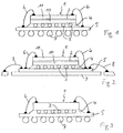
- FIG. 1 an arrangement is shown in which a semiconductor chip 1 is mounted on a substrate 5.
- the semiconductor chip 1 is composed of two individual chips: one lower first semiconductor chip 10 and an upper second Semiconductor chip 11. These semiconductor chips 10, 11 are with their Backsides, d. H. with two main pages that are no components wear, permanently attached to each other. That can e.g. B. be effected by an adhesive layer 2.
- the one with this Adhesive layers of joined surfaces are preferred provided with a respective metallization.
- connection surfaces of the substrate In this example, 5 occurs with those in FIG. 1 solder balls drawn in cross section 3.
- This type of Assembly is called flip-chip assembly and is in itself known. With this type of assembly and electrical contacting becomes a semiconductor chip with the one provided with components Top facing such a substrate that the on existing contacts on the top of the semiconductor chip face the assigned contact surfaces of the substrate. The opposite contacts are then electrically connected to each other what preferably by applied at the relevant points small amounts of a solder happen. It is in usually a soft solder, which is heated slightly when pressed, a permanent conductive connection between the connection contacts. The spaces between the solder balls 3 can by a casting compound or filling compound 4 (so-called underfill).
- connection contacts of the upper second semiconductor chip 11 on that of the substrate 5 facing away from this second semiconductor chip 11 available.
- These other connection contacts that are not already are contacted with the flip chip assembly are by means of Bond wires 6 with associated contact surfaces of the substrate electrically connected.
- Bond wires 6 with associated contact surfaces of the substrate electrically connected.
- FIG. 1 Another installation or an electrical connection of the substrate 5 can in a manner known per se by means of a solder ball arrangement 9 (BGA, ball grid Array).
- FIG. 2 shows another embodiment of the arrangement, in which the assembled semiconductor chip 1 also a first semiconductor chip 10 and a second semiconductor chip 11 is composed.
- the connection of each The back of these semiconductor chips is through in FIG. 2 again an indicated adhesive layer 2 indicated.
- the flip-chip assembly of the lower first semiconductor chip 10 is also shown schematically here by the solder balls 3 shown made. While the other connection contacts of the upper second semiconductor chips 11 again with bond wires 6 associated contact surfaces of the substrate 5 are connected, is the substrate 5 here for an external connection Lead frame attached, which over in the Shape-matched electrical conductor has the appropriate Connection contacts of the substrate 5 via others Bond wires 8 are electrically connected.
- connection contacts on the the side facing the substrate and further connection contacts on the side of the chip arrangement facing away from the substrate on the one hand through a direct electrically conductive connection in the manner of a flip-chip assembly or on the other hand via bond wires connected to associated contact surfaces of the substrate are.
- this substrate in or on further carriers or housings and the associated electrical Connections arise from the essential to the invention.
- the described Exemplary embodiments BGA package and lead package can therefore be supplemented with other types of installation.
- the assembled semiconductor chips are arranged or designed that on both main sides of the entire semiconductor chip 1 connection contacts are available.
- the arrangement according to the invention has the advantages that the upper second semiconductor chip 11 in the exemplary embodiments can be chosen larger with composite semiconductor chip 1 can be used as the lower first semiconductor chip 10.
- the side Dimensions and the thickness of the semiconductor chips do not need as in the simplified representation of FIGS. 1 and 2 agree.
- a semiconductor chip from another manufacturer can be integrated more easily because of the separate Contacting the arranged towards the substrate Connection contacts and the other on the opposite side Terminal contacts a restructuring of the arrangement of the Contact areas on the substrate 5 is easily possible.
- Compared to mounting as a flip-on-chip (flip-chip mounting of semiconductor chips on another active, i.e. H. semiconductor chip provided with integrated circuits) less chip area is required because only vertical integration is required.
Landscapes
- Wire Bonding (AREA)
Abstract
Description
- Figur 1
- zeigt eine Anordnung mit BGA.
- Figur 2
- zeigt eine Anordnung mit Lead-Frame.
- Figur 3
- zeigt eine Anordnung mit beidseitig prozessiertem Chip.
Claims (5)
- Anordnung als Gehäuse für Halbleiterchips miteinem Substrat (5) mit Kontaktflächen für elektrische Kontaktierung,einem Halbleiterchip (10) mit Anschlusskontakten, die den Kontaktflächen des Substrates (5) zugewandt sind, undelektrisch leitenden Verbindungen (3) zwischen den Kontaktflächen und den Anschlusskontakten,dadurch gekennzeichnet, dassweitere Anschlusskontakte auf der von dem Substrat (5) abgewandten Seite des Halbleiterchips (10) vorhanden sind unddie weiteren Anschlusskontakte mit Kontaktflächen des Substrates (5) über Bonddrähte (6) elektrisch leitend verbunden sind.
- Anordnung nach Anspruch 1, bei derdie weiteren Anschlusskontakte an einem weiteren Halbleiterchip (11) auf der von dem Substrat (5) abgewandten Seite des weiteren Halbleiterchips (11) vorhanden sind unddie Halbleiterchips (10, 11) mit jeweiligen Oberseiten, die den Anschlusskontakten bzw. weiteren Anschlusskontakten gegenüberliegen, aneinander befestigt sind.
- Anordnung nach Anspruch 2, bei der
die Oberseiten der Halbleiterchips (10, 11), mit denen die Halbleiterchips (10, 11) aneinander befestigt sind, jeweils mit einer Metallisierung versehen sind. - Anordnung nach einem der Ansprüche 1 bis 3, bei der
das Substrat (5) mit einer Lotkugelanordnung (9) als BGA versehen ist. - Anordnung nach einem der Ansprüche 1 bis 3, bei der das Substrat (5) mit einem Leiterrahmen (7) versehen ist.
Priority Applications (1)
| Application Number | Priority Date | Filing Date | Title |
|---|---|---|---|
| EP20000106731 EP1139411A1 (de) | 2000-03-29 | 2000-03-29 | Flip-chip Halbleiter-Anordnung mit Rückseiten-Kontaktierung |
Applications Claiming Priority (1)
| Application Number | Priority Date | Filing Date | Title |
|---|---|---|---|
| EP20000106731 EP1139411A1 (de) | 2000-03-29 | 2000-03-29 | Flip-chip Halbleiter-Anordnung mit Rückseiten-Kontaktierung |
Publications (1)
| Publication Number | Publication Date |
|---|---|
| EP1139411A1 true EP1139411A1 (de) | 2001-10-04 |
Family
ID=8168279
Family Applications (1)
| Application Number | Title | Priority Date | Filing Date |
|---|---|---|---|
| EP20000106731 Withdrawn EP1139411A1 (de) | 2000-03-29 | 2000-03-29 | Flip-chip Halbleiter-Anordnung mit Rückseiten-Kontaktierung |
Country Status (1)
| Country | Link |
|---|---|
| EP (1) | EP1139411A1 (de) |
Citations (4)
| Publication number | Priority date | Publication date | Assignee | Title |
|---|---|---|---|---|
| JPS6384128A (ja) * | 1986-09-29 | 1988-04-14 | Oki Electric Ind Co Ltd | 混成集積回路装置 |
| US5703405A (en) * | 1993-03-15 | 1997-12-30 | Motorola, Inc. | Integrated circuit chip formed from processing two opposing surfaces of a wafer |
| WO2000019531A1 (en) * | 1998-09-29 | 2000-04-06 | Conexant Systems, Inc. | Backside electrical contact structure for a module having an exposed backside |
| EP1045443A2 (de) * | 1999-04-14 | 2000-10-18 | Sharp Kabushiki Kaisha | Halbleiter und seine Herstellung |
-
2000
- 2000-03-29 EP EP20000106731 patent/EP1139411A1/de not_active Withdrawn
Patent Citations (4)
| Publication number | Priority date | Publication date | Assignee | Title |
|---|---|---|---|---|
| JPS6384128A (ja) * | 1986-09-29 | 1988-04-14 | Oki Electric Ind Co Ltd | 混成集積回路装置 |
| US5703405A (en) * | 1993-03-15 | 1997-12-30 | Motorola, Inc. | Integrated circuit chip formed from processing two opposing surfaces of a wafer |
| WO2000019531A1 (en) * | 1998-09-29 | 2000-04-06 | Conexant Systems, Inc. | Backside electrical contact structure for a module having an exposed backside |
| EP1045443A2 (de) * | 1999-04-14 | 2000-10-18 | Sharp Kabushiki Kaisha | Halbleiter und seine Herstellung |
Similar Documents
| Publication | Publication Date | Title |
|---|---|---|
| DE69325749T2 (de) | Gestapelte Mehrchip-Module und Verfahren zur Herstellung | |
| DE10250538B4 (de) | Elektronisches Bauteil als Multichipmodul und Verfahren zu dessen Herstellung | |
| DE60309422T2 (de) | Multichip-modul und Herstellungsverfahren | |
| DE102005055761B4 (de) | Leistungshalbleiterbauelement mit Halbleiterchipstapel in Brückenschaltung und Verfahren zur Herstellung desselben | |
| DE69129619T2 (de) | Halbleitervorrichtung mit einer vielzahl von anschlussstiften | |
| DE10251530B4 (de) | Stapelanordnung eines Speichermoduls | |
| DE10049551A1 (de) | Gestapeltes Halbleiterbauteil | |
| DE10142119B4 (de) | Elektronisches Bauteil und Verfahren zu seiner Herstellung | |
| DE102008048420A1 (de) | Chip-Anordnung und Verfahren zum Herstellen einer Chip-Anordnung | |
| DE10142120A1 (de) | Elektronisches Bauteil mit wenigstens zwei gestapelten Halbleiterchips sowie Verfahren zu seiner Herstellung | |
| DE102007002707A1 (de) | System-in Package-Modul | |
| DE202011110802U1 (de) | Verbesserte mikroelektronische Stapelanordnungen mit mittigen Kontakten und verbessertem wärmetechnischem Kennwert | |
| DE102004001829A1 (de) | Halbleitervorrichtung | |
| DE69524724T2 (de) | Elektronische schaltungspackung | |
| EP1614158A2 (de) | Multichipmodul mit mehreren halbleiterchips sowie leiterplatte mit mehreren komponenten | |
| DE10238781A1 (de) | Halbleitervorrichtung | |
| DE102006016345A1 (de) | Halbleitermodul mit diskreten Bauelementen und Verfahren zur Herstellung desselben | |
| DE102006001767A1 (de) | Halbleitermodul mit Halbleiterchips und Verfahren zur Herstellung desselben | |
| DE10394239B4 (de) | Verfahren zum Verpacken integrierter Schaltungen und integriertes Schaltungsgehäuse | |
| DE102005041174A1 (de) | Leistungshalbleiterbauteil mit Leitungen innerhalb eines Gehäuses | |
| DE10142117A1 (de) | Elektronisches Bauteil mit wenigstens zwei gestapelten Halbleiterchips sowie Verfahren zu seiner Herstellung | |
| DE10023823A1 (de) | Multichip-Gehäuse | |
| DE102004005586B3 (de) | Halbleiterbauteil mit einem Halbleiterchipstapel auf einer Umverdrahtungsplatte und Herstellung desselben | |
| DE19702186C2 (de) | Verfahren zur Gehäusung von integrierten Schaltkreisen | |
| DE10255289A1 (de) | Elektronisches Bauteil mit gestapelten Halbleiterchips in paralleler Anordnung und Verfahren zu dessen Herstellung |
Legal Events
| Date | Code | Title | Description |
|---|---|---|---|
| PUAI | Public reference made under article 153(3) epc to a published international application that has entered the european phase |
Free format text: ORIGINAL CODE: 0009012 |
|
| AK | Designated contracting states |
Kind code of ref document: A1 Designated state(s): DE FR GB Kind code of ref document: A1 Designated state(s): AT BE CH CY DE DK ES FI FR GB GR IE IT LI LU MC NL PT SE |
|
| AX | Request for extension of the european patent |
Free format text: AL;LT;LV;MK;RO;SI |
|
| 17P | Request for examination filed |
Effective date: 20020403 |
|
| AKX | Designation fees paid |
Free format text: DE FR GB |
|
| 17Q | First examination report despatched |
Effective date: 20020809 |
|
| STAA | Information on the status of an ep patent application or granted ep patent |
Free format text: STATUS: THE APPLICATION HAS BEEN WITHDRAWN |
|
| 18W | Application withdrawn |
Effective date: 20040827 |