EP1136890B1 - Elektrophotographisches Gerät - Google Patents
Elektrophotographisches Gerät Download PDFInfo
- Publication number
- EP1136890B1 EP1136890B1 EP01106575A EP01106575A EP1136890B1 EP 1136890 B1 EP1136890 B1 EP 1136890B1 EP 01106575 A EP01106575 A EP 01106575A EP 01106575 A EP01106575 A EP 01106575A EP 1136890 B1 EP1136890 B1 EP 1136890B1
- Authority
- EP
- European Patent Office
- Prior art keywords
- portion potential
- potential
- dark portion
- exposure
- photosensitive member
- Prior art date
- Legal status (The legal status is an assumption and is not a legal conclusion. Google has not performed a legal analysis and makes no representation as to the accuracy of the status listed.)
- Expired - Lifetime
Links
- 238000000034 method Methods 0.000 claims description 25
- 238000001514 detection method Methods 0.000 claims description 2
- 230000007423 decrease Effects 0.000 claims 1
- 230000006870 function Effects 0.000 description 29
- 238000012546 transfer Methods 0.000 description 18
- 239000000463 material Substances 0.000 description 16
- 239000004065 semiconductor Substances 0.000 description 12
- 238000010586 diagram Methods 0.000 description 8
- 238000004364 calculation method Methods 0.000 description 6
- 238000005259 measurement Methods 0.000 description 5
- 230000009467 reduction Effects 0.000 description 5
- 238000012888 cubic function Methods 0.000 description 4
- 238000012887 quadratic function Methods 0.000 description 4
- 230000008859 change Effects 0.000 description 3
- 238000006243 chemical reaction Methods 0.000 description 3
- 230000003287 optical effect Effects 0.000 description 3
- 238000013461 design Methods 0.000 description 2
- 230000008030 elimination Effects 0.000 description 2
- 238000003379 elimination reaction Methods 0.000 description 2
- 238000002474 experimental method Methods 0.000 description 2
- 239000011521 glass Substances 0.000 description 2
- 230000007246 mechanism Effects 0.000 description 2
- 230000002093 peripheral effect Effects 0.000 description 2
- 238000012545 processing Methods 0.000 description 2
- 238000000926 separation method Methods 0.000 description 2
- 230000004913 activation Effects 0.000 description 1
- 230000006866 deterioration Effects 0.000 description 1
- 238000011161 development Methods 0.000 description 1
- 238000003384 imaging method Methods 0.000 description 1
- 230000008569 process Effects 0.000 description 1
- 230000001235 sensitizing effect Effects 0.000 description 1
- 230000000087 stabilizing effect Effects 0.000 description 1
Images


Classifications
-
- G—PHYSICS
- G03—PHOTOGRAPHY; CINEMATOGRAPHY; ANALOGOUS TECHNIQUES USING WAVES OTHER THAN OPTICAL WAVES; ELECTROGRAPHY; HOLOGRAPHY
- G03G—ELECTROGRAPHY; ELECTROPHOTOGRAPHY; MAGNETOGRAPHY
- G03G15/00—Apparatus for electrographic processes using a charge pattern
- G03G15/50—Machine control of apparatus for electrographic processes using a charge pattern, e.g. regulating differents parts of the machine, multimode copiers, microprocessor control
- G03G15/5033—Machine control of apparatus for electrographic processes using a charge pattern, e.g. regulating differents parts of the machine, multimode copiers, microprocessor control by measuring the photoconductor characteristics, e.g. temperature, or the characteristics of an image on the photoconductor
- G03G15/5037—Machine control of apparatus for electrographic processes using a charge pattern, e.g. regulating differents parts of the machine, multimode copiers, microprocessor control by measuring the photoconductor characteristics, e.g. temperature, or the characteristics of an image on the photoconductor the characteristics being an electrical parameter, e.g. voltage
-
- G—PHYSICS
- G03—PHOTOGRAPHY; CINEMATOGRAPHY; ANALOGOUS TECHNIQUES USING WAVES OTHER THAN OPTICAL WAVES; ELECTROGRAPHY; HOLOGRAPHY
- G03G—ELECTROGRAPHY; ELECTROPHOTOGRAPHY; MAGNETOGRAPHY
- G03G15/00—Apparatus for electrographic processes using a charge pattern
- G03G15/04—Apparatus for electrographic processes using a charge pattern for exposing, i.e. imagewise exposure by optically projecting the original image on a photoconductive recording material
- G03G15/043—Apparatus for electrographic processes using a charge pattern for exposing, i.e. imagewise exposure by optically projecting the original image on a photoconductive recording material with means for controlling illumination or exposure
-
- H—ELECTRICITY
- H04—ELECTRIC COMMUNICATION TECHNIQUE
- H04N—PICTORIAL COMMUNICATION, e.g. TELEVISION
- H04N1/00—Scanning, transmission or reproduction of documents or the like, e.g. facsimile transmission; Details thereof
- H04N1/40—Picture signal circuits
- H04N1/407—Control or modification of tonal gradation or of extreme levels, e.g. background level
- H04N1/4076—Control or modification of tonal gradation or of extreme levels, e.g. background level dependent on references outside the picture
Definitions
- the present invention relates to an electrophotographic apparatus for controlling the surface potential of a photosensitive member, and in particular relates to an electrophotographic apparatus that can select one of multiple target potentials as the surface potential for a photosensitive member.
- a widely employed technique for setting a desired dark portion potential and a desired light portion potential for an eloectrophotographic photosensitive member involves the use of detection means, called a potential sensor, for measuring dark portion potential and light portion potential.
- the potential control is initiated either at the time of or after a predetermined time has elapsed following the activation of an image forming apparatus, before the first output or after a predetermined time has elapsed following it, or upon the receipt of an artificial execution command.
- the exposure amount of the exposure means is substantially "0"
- the charge amount of the electrification means is adjusted so as to set a desired dark portion potential
- the exposure amount (quantity) of the exposure means is determined by using the charge amount (quantity) whereat the dark portion potential was obtained.
- an exposure amount E1 is adjusted in a region wherein the inclination of the potential to the exposure amount is comparatively large, and either a specific value is added to the exposure amount or the exposure amount is multiplied by a specific rate, so that the final desired light portion potential is obtained as the second light portion potential.
- an image forming apparatus is generally employed that uses the second light portion potential to output an image. That is, the first light portion potential is detected by a sensor for the potential adjustment, and the second light portion potential is used to actually form an image.
- the second light portion potential that is, the final light portion potential
- multiple different dark portion potentials are employed to change the dark portion potential, e.g., because of an image forming difference between a copy image and a printer image, because of a reduction in the amount of toner consumed, because of the need to prevent the leakage of electrification means in a low atmosphere, because of the need to adjust an image density, or because of development characteristics due to an environment.
- the JP-A-06230642 discloses a potential controller for a photosensitive body.
- An arithmetic device sets a dark potential of the photosensitive body to a target value before forming an image, and obtains optimum light quantity to get a target light potential after obtaining the target light potential of the photosensitive body in accordance with the surface temperature of the photosensitive body, and corrects the optimum light quantity according to the surface temperature of the photosensitive body at the time of forming an image.
- the EP-A-0 338 962 discloses method steps used to initially set a printer's electrostatic parameters to achieve a specific curve.
- a desired charge corona's grid voltage Vd is calculated from a saturation voltage level Vs of a photoconductor charged to a target value of Vd and a design voltage vector.
- a photoconductor voltage Vp is calculated from the saturation voltage level Vs and a design voltage vector.
- Fig. 1 is a schematic diagram showing as a copier an image forming apparatus according to a first embodiment of the present invention.
- a cylindrical photosensitive drum 2 is provided as an electrophotographic photosensitive member.
- the photosensitive drum 2 is supported by the main body 1 so that it can be rotated in the direction indicated by an arrow R1.
- a charge elimination unit 3 such as a pre-exposure lamp, for eliminating the potential on the photosensitive drum 2
- a primary electrification device 4 as electrification means for uniformly electrifying the surface of the photosensitive drum 2
- exposure means 5 for exposing the surface of the photosensitive drum 2 and forming an electrostatic latent image
- a potential sensor 6, for measuring the surface potential of the photosensitive drum 2 after exposure
- a transfer electrification device 8 for transferring the toner image to a transferring material P
- a cleaner 10 for
- the transfer material P in the paper deck 11 is supplied by a feed roller 12, and is fed via a carry roller 13 and a resist roller 15 to a gap between the photosensitive drum 2 and the transfer electrification device 8.
- the transfer material P is then transported along a carry belt 16 to a fixing unit 17.
- the toner image is fixed to the transfer material P by heat and pressure exerted by the fixing unit 17, and the transfer material P, bearing a final copy image, is discharged by discharge rollers 19 to a discharge tray 20.
- an original document placed on a platen glass 21, is irradiated by an original lighting lamp 22 and a reflection plate 23.
- the light reflected from the original image is further reflected by mirrors 25a, 25b and 25c, and is passed through a magnification lens 26 and guided, via a projection mirror 27, to the surface of the photosensitive drum 2.
- this light is used to expose the surface of the photosensitive drum 2, which is uniformly electrified, and to form an electrostatic latent image corresponding to the original image.
- a standard white board 28 is located at the end of the platen glass 21, and the original lighting lamp 22 irradiates the white board 28 to form a light portion potential on the photosensitive drum 2.
- Fig. 2 is a schematic diagram for explaining the electric arrangement in the vicinity of the control board and determining how it affects the measurement of the potential on the photosensitive drum 2.
- a ROM in which a control program is stored
- a RAM which is a temporary storage device for storing data required for the program
- a CPU which is the central processing device.
- an I/O which is an interface device
- an A/D converter and a D/A converter which are data conversion devices
- a potential sensor is provided that can measure the potential on the photosensitive drum 2 after it has been electrified and exposed. Further, the application voltages for the primary electrification device 4 and the original lighting lamp 22 are controlled in order to form a desired dark portion and light portion potentials on the photosensitive drum 2.
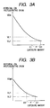
- Figs. 3A and 3B are graphs for explaining the exposure amount used to obtain a first equal light portion potential VL1 and a second equal light portion potential VL2 for two different dark portion potentials.
- the first light portion potential VL1, of 100 V is obtained at the first exposure amount E1
- the second light portion potential VL2, of 50 V is obtained at the second exposure amount E2.
- the dark portion potential VDtx in Fig. 3A , is a condition applied for a character mode of the image forming apparatus for an original document that mainly includes characters.
- the dark portion potential VDph in Fig. 3B , is a condition applied for a photo mode for an original document that mainly includes photos.
- the exposure amount E1 need only be adjusted and the obtained amount increased by a part equivalent to ⁇ .
- the exposure amount E1' need only be adjusted and be obtained amount increased by a part equivalent to ⁇ '. This is true because, as is described above, the inclination of the potential is small near E2 and E2' and it is difficult to directly adjust the exposure amounts E2 and E2', thus, the exposure amounts E1 and E1' must be obtained first and then ⁇ and ⁇ ' must be added thereto.
- ⁇ is not equal to ⁇ '.
- the exposure amount of the original lighting lamp 22 of this embodiment is determined by application of the voltage, and the differences ⁇ and ⁇ ' for the exposure amounts are 7 V and 5 V, obtained through the conversion of the voltage applied to the original lighting lamp.
- the toner reduction mode for reducing the target dark portion potential VD
- the target dark portion potential VD is simply reduced by 50 V, and then four target VDs are set: 400 V (character/standard mode), 350 V (character/toner reduction mode), 300 V (photo/standard mode), and 250 V (photo/toner reduction mode).
- the toner reduction mode when the dark portion potential is to be reduced multiple levels, the number of VDs that must be set in order to store the difference in the exposure amount is twice the count of the multiple levels. In this embodiment, the above four target dark portion potentials are included.
- the present inventor formed the dark portion potentials VD on the photosensitive drum, and adjusted the voltage P1 of the original lighting lamp, which obtains the first exposure amount E1, to obtain the first light portion potential VL1. Further, the present inventor closely examined the voltage P2 of the original lighting lamp, which obtains the second exposure amount E2, to obtain the second light portion potential. Because of the potential characteristic of the photosensitive member, a large measurement error occurs when the potential adjustment mechanism of the image forming apparatus is used, and it is difficult to measure the voltage P2 within a short period of time. Thus, for an examination of the voltage P2 of the original lighting lamp that obtains E2, an experiment was conducted that yielded a higher precision by using an external potential measurement system and increasing the number of measurements.
- Fig. 5 is a graph showing the experiment results plotted relative to the dark portion potential VD, i.e., showing the ratio P2/P1 between the voltage P2 of the original lighting lamp used to obtain the second exposure amount E2 and the voltage P1 used to obtain the first exposure amount E1.
- the ratio P2/P1 changes monotonously; it is not linear, but curved.
- the second voltage P2 is calculated using the following expression.
- Fig. 7 is a flowchart for the potential control provided for this embodiment.
- the original lighting lamp 22 is turned off and a predetermined voltage is applied to the primary electrification device 4.
- the initial applied voltage may be either a predetermined value or a previously adjusted voltage value.
- This dark portion potential is measured by the potential sensor 6, which is distant from the primary electrification device 4 and is located downstream of the photosensitive drum 2 (m2), and whether the target dark portion potential VD has been attained is determined (m3).
- the voltage that constitutes the electrification control value applied to the primary electrification device 4 is controlled (m4) so that the dark portion potential matches to the target dark portion potential VD.
- the photosensitive drum 2 is electrified by applying the voltage for the primary electrification device 4 that is determined through the above sequence, and the original lighting lamp 22 is used to irradiate the standard white board 28 to form the first light portion potential on the photosensitive drum 2 (m5).
- the voltage applied to the original lighting lamp 22 may be either a predetermined value or a value applied at a previous control time.
- the light portion potential is measured by the potential sensor 6 (m6).
- the voltage applied to the original lighting lamp 22, which is the exposure control value is changed (m8), and the exposure amount is adjusted so that the light portion potential is reset to the target portion potential VL1.
- the first voltage thus adjusted is defined as P1 (m9).
- the second applied voltage P2, which is the exposure control value for image forming is calculated using the first expression (m10).
- the second applied voltage P2 is a voltage to be applied to the original lighting lamp 22 for the copying of the actual original document.
- the second voltage P2 is provided as the function of the dark portion potential VD.
- the dark portion potential for image forming is formed by the application of the voltage P2
- the stable light portion potential VL2 can be obtained, and the obtained image can be stabilized.
- Table 1 shows a comparison between the conventional examples and the embodiment of this invention.
- Table 1 Conventional example 1 Conventional example 2 Conventional example 3 Conventional example 4 Embodiment of the invention
- P2 is represented by the functions of P1 and VD.
- conventional example 1 employs a method for fixing the exposure amount difference ⁇ in Fig. 3 , i.e., for fixing the difference (A) between the voltages applied to the original lighting lamp 22.
- This simple configuration can not cope with different dark portion potentials VD.
- Conventional example 2 also employs the method for fixing the exposure amount ratio ⁇ in Fig. 4 , i.e., for fixing the ratio (B) of the voltages applied to the original lighting lamp 22. This simple configuration also can not cope with different dark portion potentials VD.
- Conventional example 3 employs a method for storing a number of exposure amount differences ⁇ that is the equivalent of the count of the different VDs, i.e., for storing the number of differences (A) between voltages applied to the original lighting lamp 22 that is equivalent in count to the VDs that are set.
- ⁇ the number of differences between the voltages A that correspond to ⁇
- A the number of differences between the voltages A that correspond to ⁇
- Conventional example 4 employs a method for storing a number of exposure amount ratios ⁇ that is equivalent to the count of different VDs, i.e., for storing a number of the ratios (B) of voltages applied to the original lighting lamp 22 that is equivalent to the count of VDs that are set.
- the disadvantages of conventional example 4 are the same as for conventional example 3.
- the second applied voltage P2 is calculated using the function of the first applied voltage P1 and VD, this method can cope with different dark portion potential VDs that are set.
- the structural and cost problems as in conventional examples 3 and 4 do not arise, the stable light portion potential VL2 is obtained and a stable image can be formed.
- the voltage P2 applied to the original lighting lamp 22, to obtain the second light portion potential used for actual image forming is calculated by employing the product of the function of the dark portion potential and the voltage P1, applied to the original lighting lamp 22 for obtaining the first light portion potential used for adjustment.
- a digital exposure printer will now be described.
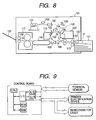
- Fig. 8 is a schematic diagram showing as a printer an image forming apparatus according to the second embodiment of the invention.
- a cylindrical photosensitive drum 102 is provided as an electrophotographic photosensitive member.
- the photosensitive drum 102 is supported so that it can be rotated in the direction indicated by an arrow R1.
- a charge elimination unit 103 such as a pre-exposure lamp, for eliminating the potential on the photosensitive drum 102
- a primary electrification device 104 for uniformly electrifying the surface of the photosensitive drum 102
- exposure means 105 for exposing the surface of the photosensitive drum 102 and forming an electrostatic latent image
- a potential sensor 106 for measuring the surface potential of the photosensitive drum 102 after exposure
- a developing device 107 as developing means for attaching toner to the electrostatic latent image and forming a toner image
- a transfer electrification device 108 for transferring the toner image to a transfer material P
- a separation electrification device 109 for separating the transfer material P
- the transfer material P to which the toner image is to be transferred, is supplied from a paper deck 111.
- This paper deck 111 for stacking the transfer materials P, is located below the photosensitive member 102, i.e., in the lower portion of the main body 101.
- the transfer material P in the paper deck 111 is supplied by a feed roller 112, and is fed via a carry roller 113 and a resist roller 115 to a gap between the photosensitive drum 102 and the transfer electrification device 108.
- the transfer material P is then transported along a carry belt 116 to a fixing unit 117.
- the toner image is fixed to the transfer material P by heat and pressure exerted by the fixing unit 117, and the transfer material P, bearing a final copy image, is discharged by discharge rollers 119 to a discharge tray 120.
- a laser beam is emitted by a semiconductor laser 130 in accordance with an image signal, is scanned by a polygon mirror 131, and is guided via an imaging lens 132 and a reflection mirror 133 to the photosensitive drum 102.
- Fig. 9 is a schematic diagram for explaining the electric arrangement in the vicinity of the control board that measures the potential on the photosensitive drum 102.
- a ROM in which a control program is stored, and a RAM, which is a temporary storage device for storing data required for the program, are connected to a CPU, which is the center processing device.
- an I/O which is an interface device, and an A/D converter and a D/A converter, which are data conversion devices, are connected to external periphery devices, and information is input to or output by the control board.
- a potential sensor can measure the potential on the photosensitive drum 102 after it has been electrified and exposed.
- the voltage to be applied to the primary electrification device 104 and the output value, which is a control value that is to be applied to the semiconductor laser 130, are controlled in order to form a desired dark portion potential and light portion potential on the photosensitive drum 102.
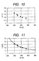
- the present inventor examined, relative to the target dark portion potential, the ratio of the output values L2 and L1 to be applied to the semiconductor laser 130.
- the output value L2 is employed for obtaining the second exposure amount E2 in order to acquire the second light portion potential VL2 used for image forming
- the output value L1 is employed for obtaining the first exposure amount E1 in order to acquire the first light portion potential VL1 used for adjustment.
- Fig. 10 is a graph showing the ratio L2/L1, obtained by the examination of the second output value L2 and the first output value L1, that is plotted relative to the dark portion potential VD.
- the ratio L2/L1 changes monotonously; it is not linear, but curved.
- the plots were substantially located along the approximate curve.
- a hyperbola was matched the most.
- each output value to be applied to the semiconductor laser 130 corresponds to each exposure amount on the photosensitive drum 102, and an approximately linear relationship is established.
- the calculation of the output value to be applied to the semiconductor laser 130 refers to the calculation of the exposure amount E2.
- Fig. 12 is a flowchart for the potential control provided for this embodiment.
- the semiconductor laser 130 is turned off and a predetermined voltage is applied to the primary electrification device 104 to form the initial dark portion potential (n1).
- the initial applied voltage may be either a predetermined value or a previously adjusted voltage value.
- This dark portion potential is measured by the potential sensor 106, which is distant from the primary electrification device 104 (n2) and is located downstream of the photosensitive drum 102, and whether the target dark portion potential VD has been attained is determined (n3).
- the voltage applied to the primary electrification device 104 is controlled (n4) so that the dark portion potential matches to the target dark portion potential VD.
- the photosensitive drum 102 is electrified by applying the voltage for the primary electrification device 104 that is determined through the above sequence, and the semiconductor laser 130 is turned on to form the first light portion potential on the photosensitive drum 102 (n5).
- the output value to be applied to the semiconductor laser 130 may be either a predetermined value or an output value used at a previous control time.
- the light portion potential is measured by the potential sensor 106 (n6).
- the output value applied to the semiconductor laser 130 is changed (n8), and the exposure amount is adjusted so that the light portion potential is reset to the target portion potential VL1.
- the output value applied to the semiconductor laser 130 at the thus adjusted first exposure amount E1 is defined as L1 (n9).
- the output value L2 which is to be applied to the semiconductor laser 130 in order to obtain the second exposure amount E2 used for image forming, is calculated using the second expression (n10).
- the output value L2 is provided as the function of the dark portion potential VD.
- the stable light portion potential VL2 can be obtained regardless of the dark portion potential VD, and the obtained image can be stabilized.
- the function of the dark portion potential is employed to calculate the exposure amount E2, or the optical physical value P2 or L2 for obtaining the exposure amount E2.
- the coefficient differs, for the first and second embodiments the hyperbola function for the dark portion potential VD is employed as this function, whereas in this embodiment, another approximate curve is employed.
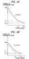
- Figs. 13A, 13B and 13C are graphs showing the results obtained when various approximate curves are employed.
- the vertical axis represents the function f[VD].
- the logarithmic curve in Fig. 13A the power function in Fig. 13B or the exponential function in Fig. 13C can be employed for the calculation.
- Fig. 14A is a graph showing the approximate curve of the quadratic function of the VD
- Fig. 14B is a graph showing the approximate curve of the cubic function of the VD.
- the coefficients for the functions of the dark portion potential VD used for the embodiment are merely examples. Optimal values need only be selected in accordance with the characteristic of the image forming apparatus, and the coefficients are not limited to those described here.
- the exposure amount E2 for obtaining the second light portion potential VL2 is obtained by using the product of the VD function and the exposure amount 1 to obtain the first light portion potential VL2, so that the accurate light portion potential VL2 can be formed and the optical image quality provided.
- the optical physical value for determining the exposure amount e.g., the voltage P2 to be applied to the original lighting lamp, may be obtained using the product of the VD function and the voltage P1 to obtain the exposure amount E1.
- the stable light portion potential VL2 can be constantly obtained even for different dark portion potentials VD.
- the invention can be employed not only for an analog exposure printer but also for a digital exposure printer.
- the output value L2 applied to the semiconductor layer can also be obtained by using the product of the function of the dark portion potential VD and the output value L1 to obtain the exposure amount E1.
- an image forming apparatus that can set multiple VDs does not require a large memory capacity in order to obtain the second light portion potential VL2, and can very easily and accurately perform potential control.
Landscapes
- Physics & Mathematics (AREA)
- General Physics & Mathematics (AREA)
- Engineering & Computer Science (AREA)
- Microelectronics & Electronic Packaging (AREA)
- Multimedia (AREA)
- Signal Processing (AREA)
- Control Or Security For Electrophotography (AREA)
- Exposure Or Original Feeding In Electrophotography (AREA)
- Electrostatic Charge, Transfer And Separation In Electrography (AREA)
Claims (10)
- Verfahren, das in einer elektrofotografischen Vorrichtung mit einem fotoleitfähigen Element (2) und einer elektrostatischen Bilderzeugungseinrichtung zur Erzeugung eines elektrostatischen Bildes auf dem fotoleitfähigen Element verwendet wird, die eine Elektrifizierungseinrichtung (4) zur Elektrifizierung des fotoleitfähigen Elements und eine Belichtungseinrichtung (5) zur Belichtung des fotoleitfähigen Elements enthält, mit
Erfassen eines Oberflächenpotentials auf dem fotoleitfähigen Element und
Bestimmen eines Elektrifizierungsbetrags für die Elektrifizierungseinrichtung (4) durch Verwenden der in dem Erfassungsschritt erhaltenen Erfassungsergebnisse,
gekennzeichnet durch
Anpassen (m2-m4; n2-n4) des Elektrifizierungsbetrags für die Elektrifizierungseinrichtung (4), wobei ein auf dem fotoleitfähigen Element (2) erzeugtes Dunkelabschnittpotential (m1; n1) im Wesentlichen ein aus vielen Solldunkelabschnittpotentialen VDtx, VDph ausgewähltes Solldunkelabschnittspotential VD ist,
Anpassen (m6-m8; n6-n8) eines an die Belichtungseinrichtung (5) angelegten ersten Belichtungssteuerungswerts P1, L1, wobei ein Hellabschnittpotential, das auf dem fotoleitfähigen Element durch die Elektrifizierungseinrichtung durch Anlegen des angepassten Elektrifizierungsbetrags und durch die Belichtungseinrichtung erzeugt wird (m5; n5), im Wesentlichen ein erstes Sollhellabschnittpotential VL1 ist, und
Berechnen (m10; n10) eines an die Belichtungseinrichtung (5) zur tatsächlichen Bilderzeugung anzulegenden zweiten Belichtungssteuerungswerts P2, L2 aus einem Produkt des ersten Belichtungssteuerungswerts P1, L1 und einer Funktion g[VD], f[VD], die das ausgewählte Solldunkelabschnittpotential VD als Variable verwendet. - Verfahren nach Anspruch 1, wobei der Belichtungssteuerungswert eine Belichtungsmenge für die Belichtungseinrichtung ist.
- Verfahren nach Anspruch 1, wobei die Belichtungseinrichtung das fotoleitfähige Element beruhend auf einem Vorlagenbild belichtet.
- Verfahren nach Anspruch 1, wobei die Belichtungseinrichtung das fotoleitfähige Element beruhend auf einem Bildsignal belichtet.
- Verfahren nach Anspruch 1, wobei die Belichtungseinrichtung einen Laser enthält, und der Belichtungssteuerungswert ein an den Laser anzulegender Ausgabewert ist.
- Verfahren nach Anspruch 1, wobei die Funktion mit Erhöhung des ausgewählten Solldunkelabschnittpotentials monoton fällt.
- Verfahren nach Anspruch 1, wobei die Funktion eine Hyperbel ist.
- Verfahren nach Anspruch 1, wobei das zweite Sollhellabschnittpotential kleiner als das erste Sollhellabschnittpotential ist.
- Verfahren nach Anspruch 1, wobei das zweite Sollhellabschnittpotential ungeachtet der vielen Solldunkelabschnittpotentiale konstant ist.
- Verfahren nach Anspruch 1, wobei ein Zeichenmodus zur Erzeugung eines Zeichenbildes und ein Fotomodus zur Erzeugung eines Fotobildes zur Auswahl verfügbar sind, und wobei das Solldunkelabschnittpotential entsprechend einem ausgewählten Modus ausgewählt wird.
Applications Claiming Priority (2)
| Application Number | Priority Date | Filing Date | Title |
|---|---|---|---|
| JP2000079313 | 2000-03-16 | ||
| JP2000079313A JP3854774B2 (ja) | 2000-03-16 | 2000-03-16 | 画像形成装置 |
Publications (3)
| Publication Number | Publication Date |
|---|---|
| EP1136890A2 EP1136890A2 (de) | 2001-09-26 |
| EP1136890A3 EP1136890A3 (de) | 2005-10-12 |
| EP1136890B1 true EP1136890B1 (de) | 2012-09-05 |
Family
ID=18596578
Family Applications (1)
| Application Number | Title | Priority Date | Filing Date |
|---|---|---|---|
| EP01106575A Expired - Lifetime EP1136890B1 (de) | 2000-03-16 | 2001-03-15 | Elektrophotographisches Gerät |
Country Status (3)
| Country | Link |
|---|---|
| US (1) | US6418280B2 (de) |
| EP (1) | EP1136890B1 (de) |
| JP (1) | JP3854774B2 (de) |
Families Citing this family (8)
| Publication number | Priority date | Publication date | Assignee | Title |
|---|---|---|---|---|
| US6987576B2 (en) * | 2000-03-06 | 2006-01-17 | Canon Kabushiki Kaisha | Image forming apparatus with gamma conversion means |
| JP2003098773A (ja) * | 2001-07-16 | 2003-04-04 | Hitachi Koki Co Ltd | 印写制御方法 |
| US6928383B2 (en) * | 2002-12-18 | 2005-08-09 | Wacom Co., Ltd. | Three-dimensional information detecting system, three-dimensional information detecting device and input device for three-dimensional information detecting system |
| JP2005189355A (ja) * | 2003-12-24 | 2005-07-14 | Canon Inc | 画像形成装置 |
| JP4810119B2 (ja) * | 2005-05-09 | 2011-11-09 | キヤノン株式会社 | 画像形成装置およびその制御方法 |
| JP4337801B2 (ja) * | 2005-10-17 | 2009-09-30 | コニカミノルタビジネステクノロジーズ株式会社 | 画像形成装置およびその露光制御方法 |
| JP2008139834A (ja) * | 2006-11-09 | 2008-06-19 | Canon Inc | 画像形成装置 |
| JP6643007B2 (ja) * | 2015-08-25 | 2020-02-12 | キヤノン株式会社 | 画像形成装置 |
Family Cites Families (13)
| Publication number | Priority date | Publication date | Assignee | Title |
|---|---|---|---|---|
| JPS6040024B2 (ja) | 1976-09-17 | 1985-09-09 | キヤノン株式会社 | 静電潜像安定化方法 |
| US4821068A (en) * | 1983-05-10 | 1989-04-11 | Canon Kabushiki Kaisha | Image forming apparatus |
| US4709250A (en) * | 1985-02-19 | 1987-11-24 | Canon Kabushiki Kaisha | Image forming apparatus |
| US4879577A (en) | 1988-04-19 | 1989-11-07 | International Business Machines Corporation | Method and apparatus for controlling the electrostatic parameters of an electrophotographic reproduction device |
| US5016050A (en) * | 1989-04-27 | 1991-05-14 | Xerox Corporation | Xerographic setup and operating system for electrostatographic reproduction machines |
| US5481337A (en) | 1991-05-13 | 1996-01-02 | Canon Kabushiki Kaisha | Method and apparatus for correcting image formation in accordance with a potential measurement and a density measurement selected along an axial direction of a photosensitive drum |
| JP3154261B2 (ja) * | 1991-09-18 | 2001-04-09 | キヤノン株式会社 | 画像形成装置 |
| JPH05142882A (ja) | 1991-11-15 | 1993-06-11 | Mita Ind Co Ltd | 複写機 |
| JPH06118759A (ja) * | 1992-10-05 | 1994-04-28 | Minolta Camera Co Ltd | 画像安定化法 |
| JPH06167853A (ja) * | 1992-11-30 | 1994-06-14 | Ricoh Co Ltd | 画像形成装置 |
| JPH06230642A (ja) | 1993-02-02 | 1994-08-19 | Fuji Xerox Co Ltd | 感光体電位制御装置 |
| JP3362068B2 (ja) * | 1993-04-28 | 2003-01-07 | 株式会社リコー | 画像形成プロセスにおける電位形成条件制御方法 |
| JPH10288874A (ja) * | 1997-04-15 | 1998-10-27 | Canon Inc | 画像形成装置 |
-
2000
- 2000-03-16 JP JP2000079313A patent/JP3854774B2/ja not_active Expired - Fee Related
-
2001
- 2001-03-13 US US09/804,155 patent/US6418280B2/en not_active Expired - Fee Related
- 2001-03-15 EP EP01106575A patent/EP1136890B1/de not_active Expired - Lifetime
Also Published As
| Publication number | Publication date |
|---|---|
| EP1136890A2 (de) | 2001-09-26 |
| US20010046390A1 (en) | 2001-11-29 |
| JP2001265074A (ja) | 2001-09-28 |
| US6418280B2 (en) | 2002-07-09 |
| EP1136890A3 (de) | 2005-10-12 |
| JP3854774B2 (ja) | 2006-12-06 |
Similar Documents
| Publication | Publication Date | Title |
|---|---|---|
| EP0535655B1 (de) | Elektrophotographisches Gerät mit Bildkontrollmitteln | |
| US5749022A (en) | Charging apparatus and method for use in image forming device | |
| US5019862A (en) | Heat control for photoreceptor | |
| JP2738749B2 (ja) | 画像形成装置 | |
| EP1136890B1 (de) | Elektrophotographisches Gerät | |
| US6647219B2 (en) | Electrophotographic recording process control method and apparatus | |
| US5045882A (en) | Xerographic setup and operating system for electrostatographic reproduction machines | |
| US5974276A (en) | Image density adjustment method for image forming apparatus | |
| US4619520A (en) | Variable magnification electrophotographic copying apparatus | |
| JP3234138B2 (ja) | 画像安定化装置 | |
| JP3097361B2 (ja) | 電子写真式複写機 | |
| US6859628B2 (en) | Image processing system and method that uses an environmental parameter value | |
| US20020172522A1 (en) | Image forming apparatus capable of correcting control coefficient used to determine electrification bias | |
| JP3854773B2 (ja) | 画像形成装置 | |
| JPH06236098A (ja) | 複写システム作動方法 | |
| JPH05302892A (ja) | 画像形成装置の濃度制御方式 | |
| JPH05333648A (ja) | プロセスコントロール方法 | |
| JPH11109688A (ja) | 感光体の電位制御方法 | |
| JP3227345B2 (ja) | 画像形成装置 | |
| JPH05306999A (ja) | 濃度検知用センサの補正装置 | |
| JPH07115487B2 (ja) | 電子写真式印字装置 | |
| JP3170272B2 (ja) | 画像濃度制御方法 | |
| JPH0746927Y2 (ja) | トナ−供給装置 | |
| JPH11133682A (ja) | 電子写真複写装置 | |
| JPH08248704A (ja) | 電子写真装置の露光量制御方法 |
Legal Events
| Date | Code | Title | Description |
|---|---|---|---|
| PUAI | Public reference made under article 153(3) epc to a published international application that has entered the european phase |
Free format text: ORIGINAL CODE: 0009012 |
|
| AK | Designated contracting states |
Kind code of ref document: A2 Designated state(s): AT BE CH CY DE DK ES FI FR GB GR IE IT LI LU MC NL PT SE TR |
|
| AX | Request for extension of the european patent |
Free format text: AL;LT;LV;MK;RO;SI |
|
| PUAL | Search report despatched |
Free format text: ORIGINAL CODE: 0009013 |
|
| AK | Designated contracting states |
Kind code of ref document: A3 Designated state(s): AT BE CH CY DE DK ES FI FR GB GR IE IT LI LU MC NL PT SE TR |
|
| AX | Request for extension of the european patent |
Extension state: AL LT LV MK RO SI |
|
| 17P | Request for examination filed |
Effective date: 20060412 |
|
| AKX | Designation fees paid |
Designated state(s): DE FR GB |
|
| 17Q | First examination report despatched |
Effective date: 20061102 |
|
| GRAP | Despatch of communication of intention to grant a patent |
Free format text: ORIGINAL CODE: EPIDOSNIGR1 |
|
| GRAS | Grant fee paid |
Free format text: ORIGINAL CODE: EPIDOSNIGR3 |
|
| GRAA | (expected) grant |
Free format text: ORIGINAL CODE: 0009210 |
|
| AK | Designated contracting states |
Kind code of ref document: B1 Designated state(s): DE FR GB |
|
| REG | Reference to a national code |
Ref country code: GB Ref legal event code: FG4D |
|
| REG | Reference to a national code |
Ref country code: DE Ref legal event code: R096 Ref document number: 60147074 Country of ref document: DE Effective date: 20121025 |
|
| PLBE | No opposition filed within time limit |
Free format text: ORIGINAL CODE: 0009261 |
|
| STAA | Information on the status of an ep patent application or granted ep patent |
Free format text: STATUS: NO OPPOSITION FILED WITHIN TIME LIMIT |
|
| 26N | No opposition filed |
Effective date: 20130606 |
|
| REG | Reference to a national code |
Ref country code: DE Ref legal event code: R097 Ref document number: 60147074 Country of ref document: DE Effective date: 20130606 |
|
| REG | Reference to a national code |
Ref country code: FR Ref legal event code: PLFP Year of fee payment: 16 |
|
| PGFP | Annual fee paid to national office [announced via postgrant information from national office to epo] |
Ref country code: GB Payment date: 20160329 Year of fee payment: 16 Ref country code: FR Payment date: 20160324 Year of fee payment: 16 |
|
| PGFP | Annual fee paid to national office [announced via postgrant information from national office to epo] |
Ref country code: DE Payment date: 20160331 Year of fee payment: 16 |
|
| REG | Reference to a national code |
Ref country code: DE Ref legal event code: R119 Ref document number: 60147074 Country of ref document: DE |
|
| GBPC | Gb: european patent ceased through non-payment of renewal fee |
Effective date: 20170315 |
|
| REG | Reference to a national code |
Ref country code: FR Ref legal event code: ST Effective date: 20171130 |
|
| PG25 | Lapsed in a contracting state [announced via postgrant information from national office to epo] |
Ref country code: FR Free format text: LAPSE BECAUSE OF NON-PAYMENT OF DUE FEES Effective date: 20170331 Ref country code: DE Free format text: LAPSE BECAUSE OF NON-PAYMENT OF DUE FEES Effective date: 20171003 |
|
| PG25 | Lapsed in a contracting state [announced via postgrant information from national office to epo] |
Ref country code: GB Free format text: LAPSE BECAUSE OF NON-PAYMENT OF DUE FEES Effective date: 20170315 |