EP1134795A1 - Verfahren zur Einstellung der Schwellenspannung eines MOS - Transistors - Google Patents
Verfahren zur Einstellung der Schwellenspannung eines MOS - Transistors Download PDFInfo
- Publication number
- EP1134795A1 EP1134795A1 EP01106383A EP01106383A EP1134795A1 EP 1134795 A1 EP1134795 A1 EP 1134795A1 EP 01106383 A EP01106383 A EP 01106383A EP 01106383 A EP01106383 A EP 01106383A EP 1134795 A1 EP1134795 A1 EP 1134795A1
- Authority
- EP
- European Patent Office
- Prior art keywords
- gate
- threshold voltage
- polysilicon
- germanium
- ions
- Prior art date
- Legal status (The legal status is an assumption and is not a legal conclusion. Google has not performed a legal analysis and makes no representation as to the accuracy of the status listed.)
- Granted
Links
Images

Classifications
-
- H—ELECTRICITY
- H10—SEMICONDUCTOR DEVICES; ELECTRIC SOLID-STATE DEVICES NOT OTHERWISE PROVIDED FOR
- H10D—INORGANIC ELECTRIC SEMICONDUCTOR DEVICES
- H10D64/00—Electrodes of devices having potential barriers
- H10D64/01—Manufacture or treatment
- H10D64/013—Manufacture or treatment of electrodes having a conductor capacitively coupled to a semiconductor by an insulator
- H10D64/01302—Manufacture or treatment of electrodes having a conductor capacitively coupled to a semiconductor by an insulator the insulator being formed after the semiconductor body, the semiconductor being silicon
- H10D64/01332—Making the insulator
- H10D64/01336—Making the insulator on single crystalline silicon, e.g. chemical oxidation using a liquid
- H10D64/01344—Making the insulator on single crystalline silicon, e.g. chemical oxidation using a liquid in a nitrogen-containing ambient, e.g. N2O oxidation
-
- H—ELECTRICITY
- H10—SEMICONDUCTOR DEVICES; ELECTRIC SOLID-STATE DEVICES NOT OTHERWISE PROVIDED FOR
- H10D—INORGANIC ELECTRIC SEMICONDUCTOR DEVICES
- H10D64/00—Electrodes of devices having potential barriers
- H10D64/01—Manufacture or treatment
- H10D64/013—Manufacture or treatment of electrodes having a conductor capacitively coupled to a semiconductor by an insulator
- H10D64/01302—Manufacture or treatment of electrodes having a conductor capacitively coupled to a semiconductor by an insulator the insulator being formed after the semiconductor body, the semiconductor being silicon
- H10D64/01332—Making the insulator
- H10D64/01336—Making the insulator on single crystalline silicon, e.g. chemical oxidation using a liquid
- H10D64/01338—Making the insulator on single crystalline silicon, e.g. chemical oxidation using a liquid with a treatment, e.g. annealing, after the formation of the conductor
-
- H—ELECTRICITY
- H10—SEMICONDUCTOR DEVICES; ELECTRIC SOLID-STATE DEVICES NOT OTHERWISE PROVIDED FOR
- H10D—INORGANIC ELECTRIC SEMICONDUCTOR DEVICES
- H10D64/00—Electrodes of devices having potential barriers
- H10D64/60—Electrodes characterised by their materials
- H10D64/66—Electrodes having a conductor capacitively coupled to a semiconductor by an insulator, e.g. MIS electrodes
- H10D64/68—Electrodes having a conductor capacitively coupled to a semiconductor by an insulator, e.g. MIS electrodes characterised by the insulator, e.g. by the gate insulator
- H10D64/681—Electrodes having a conductor capacitively coupled to a semiconductor by an insulator, e.g. MIS electrodes characterised by the insulator, e.g. by the gate insulator having a compositional variation, e.g. multilayered
- H10D64/685—Electrodes having a conductor capacitively coupled to a semiconductor by an insulator, e.g. MIS electrodes characterised by the insulator, e.g. by the gate insulator having a compositional variation, e.g. multilayered being perpendicular to the channel plane
-
- H—ELECTRICITY
- H10—SEMICONDUCTOR DEVICES; ELECTRIC SOLID-STATE DEVICES NOT OTHERWISE PROVIDED FOR
- H10D—INORGANIC ELECTRIC SEMICONDUCTOR DEVICES
- H10D64/00—Electrodes of devices having potential barriers
- H10D64/60—Electrodes characterised by their materials
- H10D64/66—Electrodes having a conductor capacitively coupled to a semiconductor by an insulator, e.g. MIS electrodes
- H10D64/68—Electrodes having a conductor capacitively coupled to a semiconductor by an insulator, e.g. MIS electrodes characterised by the insulator, e.g. by the gate insulator
- H10D64/693—Electrodes having a conductor capacitively coupled to a semiconductor by an insulator, e.g. MIS electrodes characterised by the insulator, e.g. by the gate insulator the insulator comprising nitrogen, e.g. nitrides, oxynitrides or nitrogen-doped materials
-
- H—ELECTRICITY
- H10—SEMICONDUCTOR DEVICES; ELECTRIC SOLID-STATE DEVICES NOT OTHERWISE PROVIDED FOR
- H10D—INORGANIC ELECTRIC SEMICONDUCTOR DEVICES
- H10D84/00—Integrated devices formed in or on semiconductor substrates that comprise only semiconducting layers, e.g. on Si wafers or on GaAs-on-Si wafers
- H10D84/01—Manufacture or treatment
- H10D84/0123—Integrating together multiple components covered by H10D12/00 or H10D30/00, e.g. integrating multiple IGBTs
- H10D84/0126—Integrating together multiple components covered by H10D12/00 or H10D30/00, e.g. integrating multiple IGBTs the components including insulated gates, e.g. IGFETs
- H10D84/0165—Integrating together multiple components covered by H10D12/00 or H10D30/00, e.g. integrating multiple IGBTs the components including insulated gates, e.g. IGFETs the components including complementary IGFETs, e.g. CMOS devices
- H10D84/0172—Manufacturing their gate conductors
- H10D84/0177—Manufacturing their gate conductors the gate conductors having different materials or different implants
-
- H—ELECTRICITY
- H10—SEMICONDUCTOR DEVICES; ELECTRIC SOLID-STATE DEVICES NOT OTHERWISE PROVIDED FOR
- H10D—INORGANIC ELECTRIC SEMICONDUCTOR DEVICES
- H10D84/00—Integrated devices formed in or on semiconductor substrates that comprise only semiconducting layers, e.g. on Si wafers or on GaAs-on-Si wafers
- H10D84/01—Manufacture or treatment
- H10D84/02—Manufacture or treatment characterised by using material-based technologies
- H10D84/03—Manufacture or treatment characterised by using material-based technologies using Group IV technology, e.g. silicon technology or silicon-carbide [SiC] technology
- H10D84/038—Manufacture or treatment characterised by using material-based technologies using Group IV technology, e.g. silicon technology or silicon-carbide [SiC] technology using silicon technology, e.g. SiGe
-
- H—ELECTRICITY
- H10—SEMICONDUCTOR DEVICES; ELECTRIC SOLID-STATE DEVICES NOT OTHERWISE PROVIDED FOR
- H10D—INORGANIC ELECTRIC SEMICONDUCTOR DEVICES
- H10D84/00—Integrated devices formed in or on semiconductor substrates that comprise only semiconducting layers, e.g. on Si wafers or on GaAs-on-Si wafers
- H10D84/80—Integrated devices formed in or on semiconductor substrates that comprise only semiconducting layers, e.g. on Si wafers or on GaAs-on-Si wafers characterised by the integration of at least one component covered by groups H10D12/00 or H10D30/00, e.g. integration of IGFETs
- H10D84/82—Integrated devices formed in or on semiconductor substrates that comprise only semiconducting layers, e.g. on Si wafers or on GaAs-on-Si wafers characterised by the integration of at least one component covered by groups H10D12/00 or H10D30/00, e.g. integration of IGFETs of only field-effect components
- H10D84/83—Integrated devices formed in or on semiconductor substrates that comprise only semiconducting layers, e.g. on Si wafers or on GaAs-on-Si wafers characterised by the integration of at least one component covered by groups H10D12/00 or H10D30/00, e.g. integration of IGFETs of only field-effect components of only insulated-gate FETs [IGFET]
- H10D84/85—Complementary IGFETs, e.g. CMOS
- H10D84/858—Complementary IGFETs, e.g. CMOS comprising a P-type well but not an N-type well
-
- H—ELECTRICITY
- H10—SEMICONDUCTOR DEVICES; ELECTRIC SOLID-STATE DEVICES NOT OTHERWISE PROVIDED FOR
- H10D—INORGANIC ELECTRIC SEMICONDUCTOR DEVICES
- H10D64/00—Electrodes of devices having potential barriers
- H10D64/60—Electrodes characterised by their materials
- H10D64/66—Electrodes having a conductor capacitively coupled to a semiconductor by an insulator, e.g. MIS electrodes
- H10D64/667—Electrodes having a conductor capacitively coupled to a semiconductor by an insulator, e.g. MIS electrodes the conductor comprising a layer of alloy material, compound material or organic material contacting the insulator, e.g. TiN workfunction layers
Definitions
- the invention relates to a method for adjusting the Threshold voltage for a MOS transistor, in particular for the manufacture of CMOS circuits.
- a MOS transistor is a field effect transistor with an insulated control electrode or gate for driving a current channel in a substrate.
- the charge carrier density in the semiconductor substrate is controlled by the voltage applied to the gate connection. If a sufficiently high voltage is applied to the gate electrode, which exceeds a certain threshold voltage, an inversion current channel through which a current can flow is generated on the semiconductor surface between the drain connection and the source connection of the MOSFET.
- the gate voltage which is necessary in order to form the inversion current channel straight is referred to as the threshold voltage U T of the MOSFET.
- the semiconductor substrate is simultaneously Integrated n- and p-channel MOS field-effect transistors.
- a conventional CMOS manufacturing process in a p-type semiconductor substrate, for example an n-well diffuses in and then selective field oxidation performed to make the individual transistor regions superficial isolate from each other. Thereupon becomes a thin oxide layer formed, which acts as a scatter oxide. Using ion implantation then the threshold voltages of the PMOS transistors and the NMOS transistors set.
- the litter oxide is first removed, then the gate oxide is generated, and then polycrystalline silicon layers applied for the gate connections, and structured as well as after electrical isolation of the gate stack of the drain and source areas using a spacer Diffusion of acceptors for the drain connection and the source connection of the PMOS transistor and a diffusion of donors for the drain connection and source connection of the NMOS carried out. After opening the contact window by etching the drain and source areas can be contacted.
- the coordination of the threshold voltage U T of the PMOS transistor and the complementary NMOS transistor of the CMOS circuit is of particular importance, since the threshold voltage of the two complementary transistors should be the same.
- the threshold voltage depends on the work function at the gate connections.
- the work function is the energy required to release an electron from a crystal structure.
- the gate electrodes are conventionally formed from crystalline polysilicon.
- the work function and thus the threshold voltage U T of the MOSFET is set by doping the polycrystalline silicon.
- the threshold voltage U T is typically between 0.5 volts and 0.7 volts.
- the invention provides a method for adjusting the Threshold voltage for a MOS transistor made of polysilicon has an existing gate, with germanium ions in the gate to change the work function of the polysilicon existing gates are implanted.
- the gate made of polysilicon is annealed or heat-treated, by giving it a high for a period of time Exposed to temperature.
- the method is preferably used to adjust the threshold voltage of a PMOS transistor in a CMOS circuit used.
- the temperature for heat treatment of the gate after Implantation is preferably above 1000 ° C.
- the proportion of germanium in the polysilicon Gate implanted is preferably about 20%.
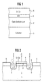
- a gate dielectric 2 is first applied to a semiconductor substrate 1 by thermal oxidation of the substrate 1 or by a deposition process.
- the dielectric 2 preferably consists of an oxide with a relatively high dielectric constant.
- the gate dielectric 2 can alternatively also be made from silicon nitride.
- Polycrystalline silicon is then applied to the gate dielectric 2 to form a gate control electrode.
- Nitrogen ions are implanted in this polysilicon layer by ion implantation. Subsequently, the polysilicon implanted with nitrogen ions is annealed by being exposed to a high temperature of over 1000 ° C. for a predetermined period of time.
- an oxidation barrier layer 3 composed of silicon and nitrogen is formed at the interface of the polysilicon layer with the gate dielectric 2.
- Germanium ions are then implanted in the remaining polysilicon layer above, in order to change the work function of the gate consisting of polysilicon.
- the implantation of the germanium ions initially creates an amorphous silicon layer, which is subsequently converted into a polycrystalline silicon-germanium compound by subsequently annealing or annealing at over 1000 ° C. in an oven.
- the germanium-doped polysilicon layer 4 forms the gate connection of the MOS transistor, the threshold voltage U T , at which an inversion layer forms in the substrate 1, being set by the percentage of germanium in the polysilicon.
- FIG. 2 shows a PMOS transistor, the threshold voltage U T of which is set by implanting germanium ions in the gate.
- the PMOS transistor has an n-doped semiconductor substrate 1, with a p + -doped drain region 5 and a p + -doped source region 6.
- the drain region 5 and the source region 6 are each electrically contacted from connections 7, 8 consisting of polysilicon.
- the semiconductor substrate 1 is otherwise covered with field oxide 9.
- the NMOS transistor has a gate 10 made of polysilicon, which is separated from a p-doped well region 12 by a dielectric 11.
- the p-doped well 12 is located in the n-doped semiconductor substrate 1.
- the NMOS transistor has an n + -doped drain region 13 and an n + -doped source region 14.
- the drain region 13 and the source region 14 can each be electrically contacted via polysilicon connections 15, 16.
- the threshold voltage U TP of the PMOS transistor can be matched to the threshold voltage U TN of the NMOS transistor by local germanium ion implantation in the gate 3 of the PMOS transistor of the CMOS circuit shown in FIG. 3.
- the threshold voltage U TN of the NMOS transistor is achieved, as in the conventional manufacturing processes, by n + doping of the gate 10 made of polysilicon. Germanium ions are only implanted in the polysilicon layer in the area of the PMOS transistor and not in the area of the NMOS transistor.
- the ion implantation allows the doping concentration of the germanium ions and thus the threshold voltage U T to be set very precisely.
- concentration profiles can also be largely controlled according to shape and location.
- the process temperatures can be kept so low that a diffusion of harmful contaminants is excluded.
- the structural changes brought about by the ion implantation in the semiconductor crystal can be compensated for by subsequent annealing by means of heat treatment.
- the short channel properties of the PMOS transistor improved without that Manufacturing process for the NMOS transistor are changed got to.
- the gate 10 made of polysilicon is NMOS transistor and the silicon gate implanted from germanium ions 4 of the PMOS transistor in a deposition and Etching process, which makes the manufacturing process a CMOS structure is significantly simplified.
- the implantation with germanium ions after the second deposition destroyed at the same time the silicon oxide that occurs between the deposition processes has formed.
- Through a two-stage polysilicon deposition with germanium ion implantation and subsequent healing leads to an improvement in germanium depletion effects at the gate-gate oxide interface.
Landscapes
- Metal-Oxide And Bipolar Metal-Oxide Semiconductor Integrated Circuits (AREA)
- Insulated Gate Type Field-Effect Transistor (AREA)
Abstract
Description
Claims (7)
- Verfahren zur Einstellung der Schwellenspannung eines MOS-Transistors, der ein aus Polysilizium bestehendes Gate aufweist, bei dem Germaniumionen in das aus Polysilizium bestehende Gate (4) zur Änderung der Austrittsarbeit des Gates implantiert werden.
- Verfahren zur Einstellung der Schwellenspannung eines MOS-Transistors, bei dem das mit Germaniumionen implantierte Gate (4) anschließend durch Wärmebehandlung ausgeheilt wird, indem es für eine vorbestimmte Zeitdauer einer hohen Temperatur ausgesetzt wird.
- Verfahren nach Anspruch 1 oder 2, bei dem vor der Implantation der Germaniumionen Stickstoffionen in das aus Polysilizium bestehende Gate (4) zur Ausbildung einer Oxidationssperrschicht implantiert werden.
- Verfahren nach Anspruch 3,
dadurch gekennzeichnet, dass nach der Implantation der Stickstoffionen das aus Polysilizium bestehende Gate zur Ausheilung wärmebehandelt wird, indem es für eine bestimmte Zeitdauer einer hohen Temperatur ausgesetzt wird. - Verfahren nach einem der vorangehenden Ansprüche,
dadurch gekennzeichnet, dass die Schwellenspannung eines PMOS-Transistors oder eines NMOS-Transistors in einer CMOS-Schaltung eingestellt wird. - Verfahren nach einem der vorangehenden Ansprüche,
dadurch gekennzeichnet, dass die Temperatur bei der Wärmebehandlung über 1000°C liegt. - Verfahren nach einem der vorangehenden Ansprüche,
dadurch gekennzeichnet, dass der Germaniumanteil des Gates (4) nach der Implantation der Germaniumionen etwa 20% beträgt.
Applications Claiming Priority (2)
| Application Number | Priority Date | Filing Date | Title |
|---|---|---|---|
| DE10014916 | 2000-03-17 | ||
| DE10014916A DE10014916C2 (de) | 2000-03-17 | 2000-03-17 | Verfahren zur Einstellung der Schwellenspannung eines MOS-Transistors |
Publications (2)
| Publication Number | Publication Date |
|---|---|
| EP1134795A1 true EP1134795A1 (de) | 2001-09-19 |
| EP1134795B1 EP1134795B1 (de) | 2003-07-30 |
Family
ID=7636377
Family Applications (1)
| Application Number | Title | Priority Date | Filing Date |
|---|---|---|---|
| EP01106383A Expired - Lifetime EP1134795B1 (de) | 2000-03-17 | 2001-03-19 | Verfahren zur Einstellung der Schwellenspannung eines MOS - Transistors |
Country Status (4)
| Country | Link |
|---|---|
| US (1) | US6451676B2 (de) |
| EP (1) | EP1134795B1 (de) |
| DE (2) | DE10014916C2 (de) |
| TW (1) | TW501204B (de) |
Families Citing this family (11)
| Publication number | Priority date | Publication date | Assignee | Title |
|---|---|---|---|---|
| JP2001358233A (ja) * | 2000-06-15 | 2001-12-26 | Hitachi Ltd | 半導体集積回路装置および半導体集積回路装置の製造方法 |
| KR100402381B1 (ko) * | 2001-02-09 | 2003-10-17 | 삼성전자주식회사 | 게르마늄 함유 폴리실리콘 게이트를 가지는 씨모스형반도체 장치 및 그 형성방법 |
| US6867101B1 (en) * | 2001-04-04 | 2005-03-15 | Advanced Micro Devices, Inc. | Method of fabricating a semiconductor device having a nitride/high-k/nitride gate dielectric stack by atomic layer deposition (ALD) and a device thereby formed |
| US6709912B1 (en) * | 2002-10-08 | 2004-03-23 | Chartered Semiconductor Manufacturing Ltd. | Dual Si-Ge polysilicon gate with different Ge concentrations for CMOS device optimization |
| US7101746B2 (en) * | 2003-11-05 | 2006-09-05 | Chartered Semiconductor Manufacturing Ltd. | Method to lower work function of gate electrode through Ge implantation |
| JP3998665B2 (ja) * | 2004-06-16 | 2007-10-31 | 株式会社ルネサステクノロジ | 半導体装置およびその製造方法 |
| US7772063B2 (en) * | 2004-08-11 | 2010-08-10 | Identifi Technologies, Inc. | Reduced-step CMOS processes for low-cost radio frequency identification devices |
| US20060172480A1 (en) * | 2005-02-03 | 2006-08-03 | Taiwan Semiconductor Manufacturing Company, Ltd. | Single metal gate CMOS device design |
| US9219078B2 (en) | 2013-04-18 | 2015-12-22 | International Business Machines Corporation | Simplified multi-threshold voltage scheme for fully depleted SOI MOSFETs |
| US9812449B2 (en) | 2015-11-20 | 2017-11-07 | Samsung Electronics Co., Ltd. | Multi-VT gate stack for III-V nanosheet devices with reduced parasitic capacitance |
| US11728383B2 (en) * | 2020-09-25 | 2023-08-15 | Applied Materials, Inc. | Localized stressor formation by ion implantation |
Citations (5)
| Publication number | Priority date | Publication date | Assignee | Title |
|---|---|---|---|---|
| US5426069A (en) * | 1992-04-09 | 1995-06-20 | Dalsa Inc. | Method for making silicon-germanium devices using germanium implantation |
| EP0707346A1 (de) * | 1994-10-11 | 1996-04-17 | Advanced Micro Devices, Inc. | Verfahren zur Herstellung einer integrierten Schaltungsanordnung |
| US5633177A (en) * | 1993-11-08 | 1997-05-27 | Advanced Micro Devices, Inc. | Method for producing a semiconductor gate conductor having an impurity migration barrier |
| US5888867A (en) * | 1998-02-13 | 1999-03-30 | Advanced Micro Devices, Inc. | Non-uniform threshold voltage adjustment in flash eproms through gate work function alteration |
| US6114206A (en) * | 1998-11-06 | 2000-09-05 | Advanced Micro Devices, Inc. | Multiple threshold voltage transistor implemented by a damascene process |
Family Cites Families (6)
| Publication number | Priority date | Publication date | Assignee | Title |
|---|---|---|---|---|
| US5374566A (en) * | 1993-01-27 | 1994-12-20 | National Semiconductor Corporation | Method of fabricating a BiCMOS structure |
| JPH07335870A (ja) * | 1994-06-14 | 1995-12-22 | Mitsubishi Electric Corp | 半導体装置およびその製造方法 |
| US5675176A (en) * | 1994-09-16 | 1997-10-07 | Kabushiki Kaisha Toshiba | Semiconductor device and a method for manufacturing the same |
| US5879996A (en) * | 1996-09-18 | 1999-03-09 | Micron Technology, Inc. | Silicon-germanium devices for CMOS formed by ion implantation and solid phase epitaxial regrowth |
| US6208004B1 (en) * | 1998-08-19 | 2001-03-27 | Philips Semiconductor, Inc. | Semiconductor device with high-temperature-stable gate electrode for sub-micron applications and fabrication thereof |
| US6180499B1 (en) * | 1998-09-29 | 2001-01-30 | Advanced Micro Devices, Inc. | Method for forming polysilicon-germanium gate in CMOS transistor and device made thereby |
-
2000
- 2000-03-17 DE DE10014916A patent/DE10014916C2/de not_active Expired - Fee Related
-
2001
- 2001-03-19 EP EP01106383A patent/EP1134795B1/de not_active Expired - Lifetime
- 2001-03-19 US US09/811,799 patent/US6451676B2/en not_active Expired - Lifetime
- 2001-03-19 DE DE50100425T patent/DE50100425D1/de not_active Expired - Lifetime
- 2001-06-13 TW TW090106207A patent/TW501204B/zh not_active IP Right Cessation
Patent Citations (5)
| Publication number | Priority date | Publication date | Assignee | Title |
|---|---|---|---|---|
| US5426069A (en) * | 1992-04-09 | 1995-06-20 | Dalsa Inc. | Method for making silicon-germanium devices using germanium implantation |
| US5633177A (en) * | 1993-11-08 | 1997-05-27 | Advanced Micro Devices, Inc. | Method for producing a semiconductor gate conductor having an impurity migration barrier |
| EP0707346A1 (de) * | 1994-10-11 | 1996-04-17 | Advanced Micro Devices, Inc. | Verfahren zur Herstellung einer integrierten Schaltungsanordnung |
| US5888867A (en) * | 1998-02-13 | 1999-03-30 | Advanced Micro Devices, Inc. | Non-uniform threshold voltage adjustment in flash eproms through gate work function alteration |
| US6114206A (en) * | 1998-11-06 | 2000-09-05 | Advanced Micro Devices, Inc. | Multiple threshold voltage transistor implemented by a damascene process |
Non-Patent Citations (3)
| Title |
|---|
| LI V Z -Q ET AL: "SINGLE GATE 0.15 MUM CMOS DEVICES FABRICATED USING RTCVD IN-SITU BORON DOPED SI1-XGEX GATES", WASHINGTON, DC, DEC. 7 - 10, 1997,NEW YORK, NY: IEEE,US, 7 December 1997 (1997-12-07), pages 833 - 836, XP000855922, ISBN: 0-7803-4101-5 * |
| TSU-JAE KING ET AL: "A VARIABLE-WORK-FUNCTION POLYCRYSTALLINE-SI1-XGEX GATE MATERIAL FOR SUBMICROMETER CMOS TECHNOLOGIES", IEEE ELECTRON DEVICE LETTERS,US,IEEE INC. NEW YORK, vol. 12, no. 10, 1 October 1991 (1991-10-01), pages 533 - 535, XP000226014, ISSN: 0741-3106 * |
| YU B ET AL: "GATE ENGINEERING FOR DEEP-SUBMICRON CMOS TRANSISTORS", IEEE TRANSACTIONS ON ELECTRON DEVICES,US,IEEE INC. NEW YORK, vol. 45, no. 6, 1 June 1998 (1998-06-01), pages 1253 - 1261, XP000754177, ISSN: 0018-9383 * |
Also Published As
| Publication number | Publication date |
|---|---|
| US6451676B2 (en) | 2002-09-17 |
| EP1134795B1 (de) | 2003-07-30 |
| DE10014916A1 (de) | 2001-10-04 |
| DE50100425D1 (de) | 2003-09-04 |
| TW501204B (en) | 2002-09-01 |
| DE10014916C2 (de) | 2002-01-24 |
| US20010023116A1 (en) | 2001-09-20 |
Similar Documents
| Publication | Publication Date | Title |
|---|---|---|
| DE10214066B4 (de) | Halbleiterbauelement mit retrogradem Dotierprofil in einem Kanalgebiet und Verfahren zur Herstellung desselben | |
| DE4229574C2 (de) | Feldeffekttransistor und Verfahren zu dessen Herstellung | |
| EP0244607B1 (de) | Verfahren zum Herstellen von optimierten komplementären MOS-Feldeffekttransistoren in VLSI-Technik | |
| DE3019850C2 (de) | ||
| EP0248988B1 (de) | Verfahren zum Herstellen von hochintegrierten komplementären MOS-Feldeffekttransistorschaltungen | |
| US5880502A (en) | Low and high voltage CMOS devices and process for fabricating same | |
| DE69835203T2 (de) | Herstellungsverfahren für nmos und pmos bauelemente mit reduzierte maskierungsschritten | |
| DE69710609T2 (de) | Herstellungsverfahern eines integrierten schaltkreises mit unterschiedlicher gateoxidedicke | |
| DE19544945A1 (de) | PMOS-Feldeffekt-Transistoren mit Indium- oder Gallium-dotierten, eingebetteten Kanälen und N+-Polysilizium-Gates aus polykristallinem Silizium und daraus hergestellte CMOS-Einrichtungen | |
| DE69514307T2 (de) | Verfahren zur Herstellung einer integrierten Schaltungsanordnung | |
| DE2700873A1 (de) | Verfahren zur herstellung von komplementaeren isolierschicht-feldeffekttransistoren | |
| DE102008049725B4 (de) | CMOS-Bauelement mit NMOS-Transistoren und PMOS-Transistoren mit stärkeren verformungsinduzierenden Quellen und Metallsilizidgebieten mit geringem Abstand und Verfahren zur Herstellung des Bauelements | |
| DE19611959C2 (de) | Komplementär-MOS-Feldeffekttransistor und Herstellungsverfahren für denselben | |
| DE69938381T2 (de) | Herstellung einer LDD Struktur für eine Schutzschaltung gegen elektrostatische Entladungen (ESD) | |
| DE60028847T2 (de) | Verfahren mit reduzierter Maskenzahl für die Herstellung von Mischsspannung-CMOS mit Hochleistung-Transistoren und -I/O Transistoren von hoher Zuverlässigkeit | |
| EP1134795B1 (de) | Verfahren zur Einstellung der Schwellenspannung eines MOS - Transistors | |
| DE69231832T2 (de) | Halbleiteranordnung ausgerüstet mit einem Hochspannungs-MISFET | |
| DE102010040064B4 (de) | Verringerte Schwellwertspannungs-Breitenabhängigkeit in Transistoren, die Metallgateelektrodenstrukturen mit großem ε aufweisen | |
| DE102015106185A1 (de) | Halbleiterstruktur und Verfahren zur Verarbeitung eines Trägers | |
| DE69105621T2 (de) | Herstellungsverfahren eines Kanals in MOS-Halbleiteranordnung. | |
| DE69519016T2 (de) | Hochspannungs-ldd-mosfet mit erhöhter durchbruchspannung und herstellungsverfahren | |
| EP0159617A1 (de) | Verfahren zum Herstellen von hochintegrierten MOS-Feldeffekttransistoren | |
| DE68916401T2 (de) | Feldeffekttransistor auf einem Isolator und Verfahren zu seiner Herstellung. | |
| DE10058031B4 (de) | Verfahren zur Bildung leicht dotierter Halogebiete und Erweiterungsgebiete in einem Halbleiterbauelement | |
| DE2854073A1 (de) | Feldeffekttransistor-anordnung sowie verfahren zu ihrer herstellung |
Legal Events
| Date | Code | Title | Description |
|---|---|---|---|
| PUAI | Public reference made under article 153(3) epc to a published international application that has entered the european phase |
Free format text: ORIGINAL CODE: 0009012 |
|
| AK | Designated contracting states |
Kind code of ref document: A1 Designated state(s): DE FR GB IE IT Kind code of ref document: A1 Designated state(s): AT BE CH CY DE DK ES FI FR GB GR IE IT LI LU MC NL PT SE TR |
|
| AX | Request for extension of the european patent |
Free format text: AL;LT;LV;MK;RO;SI |
|
| 17P | Request for examination filed |
Effective date: 20020314 |
|
| AKX | Designation fees paid |
Free format text: DE FR GB IE IT |
|
| 17Q | First examination report despatched |
Effective date: 20020807 |
|
| GRAH | Despatch of communication of intention to grant a patent |
Free format text: ORIGINAL CODE: EPIDOS IGRA |
|
| GRAA | (expected) grant |
Free format text: ORIGINAL CODE: 0009210 |
|
| GRAH | Despatch of communication of intention to grant a patent |
Free format text: ORIGINAL CODE: EPIDOS IGRA |
|
| AK | Designated contracting states |
Designated state(s): DE FR GB IE IT |
|
| REG | Reference to a national code |
Ref country code: GB Ref legal event code: FG4D Free format text: NOT ENGLISH |
|
| REG | Reference to a national code |
Ref country code: IE Ref legal event code: FG4D Free format text: GERMAN |
|
| REF | Corresponds to: |
Ref document number: 50100425 Country of ref document: DE Date of ref document: 20030904 Kind code of ref document: P |
|
| GBT | Gb: translation of ep patent filed (gb section 77(6)(a)/1977) |
Effective date: 20031111 |
|
| ET | Fr: translation filed | ||
| PLBE | No opposition filed within time limit |
Free format text: ORIGINAL CODE: 0009261 |
|
| STAA | Information on the status of an ep patent application or granted ep patent |
Free format text: STATUS: NO OPPOSITION FILED WITHIN TIME LIMIT |
|
| 26N | No opposition filed |
Effective date: 20040504 |
|
| PGFP | Annual fee paid to national office [announced via postgrant information from national office to epo] |
Ref country code: GB Payment date: 20070322 Year of fee payment: 7 |
|
| PGFP | Annual fee paid to national office [announced via postgrant information from national office to epo] |
Ref country code: IE Payment date: 20080321 Year of fee payment: 8 Ref country code: IT Payment date: 20080326 Year of fee payment: 8 |
|
| GBPC | Gb: european patent ceased through non-payment of renewal fee |
Effective date: 20080319 |
|
| PG25 | Lapsed in a contracting state [announced via postgrant information from national office to epo] |
Ref country code: GB Free format text: LAPSE BECAUSE OF NON-PAYMENT OF DUE FEES Effective date: 20080319 |
|
| PGFP | Annual fee paid to national office [announced via postgrant information from national office to epo] |
Ref country code: FR Payment date: 20081217 Year of fee payment: 10 |
|
| REG | Reference to a national code |
Ref country code: IE Ref legal event code: MM4A |
|
| PG25 | Lapsed in a contracting state [announced via postgrant information from national office to epo] |
Ref country code: IE Free format text: LAPSE BECAUSE OF NON-PAYMENT OF DUE FEES Effective date: 20090319 |
|
| REG | Reference to a national code |
Ref country code: FR Ref legal event code: ST Effective date: 20100831 |
|
| PG25 | Lapsed in a contracting state [announced via postgrant information from national office to epo] |
Ref country code: FR Free format text: LAPSE BECAUSE OF NON-PAYMENT OF DUE FEES Effective date: 20090331 |
|
| PG25 | Lapsed in a contracting state [announced via postgrant information from national office to epo] |
Ref country code: IT Free format text: LAPSE BECAUSE OF NON-PAYMENT OF DUE FEES Effective date: 20090319 |
|
| REG | Reference to a national code |
Ref country code: DE Ref legal event code: R081 Ref document number: 50100425 Country of ref document: DE Owner name: INFINEON TECHNOLOGIES AG, DE Free format text: FORMER OWNER: QIMONDA AG, 81739 MUENCHEN, DE Ref country code: DE Ref legal event code: R081 Ref document number: 50100425 Country of ref document: DE Owner name: POLARIS INNOVATIONS LTD., IE Free format text: FORMER OWNER: QIMONDA AG, 81739 MUENCHEN, DE |
|
| REG | Reference to a national code |
Ref country code: DE Ref legal event code: R081 Ref document number: 50100425 Country of ref document: DE Owner name: POLARIS INNOVATIONS LTD., IE Free format text: FORMER OWNER: INFINEON TECHNOLOGIES AG, 85579 NEUBIBERG, DE |
|
| PGFP | Annual fee paid to national office [announced via postgrant information from national office to epo] |
Ref country code: DE Payment date: 20150818 Year of fee payment: 15 |
|
| REG | Reference to a national code |
Ref country code: DE Ref legal event code: R119 Ref document number: 50100425 Country of ref document: DE |
|
| PG25 | Lapsed in a contracting state [announced via postgrant information from national office to epo] |
Ref country code: DE Free format text: LAPSE BECAUSE OF NON-PAYMENT OF DUE FEES Effective date: 20161001 |