US5675176A - Semiconductor device and a method for manufacturing the same - Google Patents
Semiconductor device and a method for manufacturing the same Download PDFInfo
- Publication number
- US5675176A US5675176A US08/530,721 US53072195A US5675176A US 5675176 A US5675176 A US 5675176A US 53072195 A US53072195 A US 53072195A US 5675176 A US5675176 A US 5675176A
- Authority
- US
- United States
- Prior art keywords
- region
- groove
- semiconductor
- semiconductor substrate
- crystal defect
- Prior art date
- Legal status (The legal status is an assumption and is not a legal conclusion. Google has not performed a legal analysis and makes no representation as to the accuracy of the status listed.)
- Expired - Lifetime
Links
- 239000004065 semiconductor Substances 0.000 title claims abstract description 234
- 238000000034 method Methods 0.000 title claims description 55
- 238000004519 manufacturing process Methods 0.000 title description 26
- 230000007547 defect Effects 0.000 claims abstract description 145
- 239000000758 substrate Substances 0.000 claims abstract description 145
- 239000013078 crystal Substances 0.000 claims abstract description 93
- 239000000126 substance Substances 0.000 claims abstract description 24
- 239000012535 impurity Substances 0.000 claims description 76
- 238000002955 isolation Methods 0.000 claims description 59
- XUIMIQQOPSSXEZ-UHFFFAOYSA-N Silicon Chemical compound [Si] XUIMIQQOPSSXEZ-UHFFFAOYSA-N 0.000 claims description 26
- 229910052710 silicon Inorganic materials 0.000 claims description 26
- 239000010703 silicon Substances 0.000 claims description 26
- 229910052796 boron Inorganic materials 0.000 claims description 17
- 238000005468 ion implantation Methods 0.000 claims description 14
- 229910052785 arsenic Inorganic materials 0.000 claims description 13
- 229910052698 phosphorus Inorganic materials 0.000 claims description 8
- 239000011574 phosphorus Substances 0.000 claims description 8
- 238000012545 processing Methods 0.000 claims description 8
- ZOXJGFHDIHLPTG-UHFFFAOYSA-N Boron Chemical compound [B] ZOXJGFHDIHLPTG-UHFFFAOYSA-N 0.000 claims description 5
- RQNWIZPPADIBDY-UHFFFAOYSA-N arsenic atom Chemical compound [As] RQNWIZPPADIBDY-UHFFFAOYSA-N 0.000 claims description 5
- XKRFYHLGVUSROY-UHFFFAOYSA-N Argon Chemical compound [Ar] XKRFYHLGVUSROY-UHFFFAOYSA-N 0.000 claims description 4
- IJGRMHOSHXDMSA-UHFFFAOYSA-N Atomic nitrogen Chemical compound N#N IJGRMHOSHXDMSA-UHFFFAOYSA-N 0.000 claims description 4
- 230000015572 biosynthetic process Effects 0.000 claims description 4
- 239000011810 insulating material Substances 0.000 claims description 4
- OAICVXFJPJFONN-UHFFFAOYSA-N Phosphorus Chemical compound [P] OAICVXFJPJFONN-UHFFFAOYSA-N 0.000 claims description 3
- 229910052787 antimony Inorganic materials 0.000 claims description 2
- WATWJIUSRGPENY-UHFFFAOYSA-N antimony atom Chemical compound [Sb] WATWJIUSRGPENY-UHFFFAOYSA-N 0.000 claims description 2
- 229910052786 argon Inorganic materials 0.000 claims description 2
- 229910052732 germanium Inorganic materials 0.000 claims description 2
- GNPVGFCGXDBREM-UHFFFAOYSA-N germanium atom Chemical compound [Ge] GNPVGFCGXDBREM-UHFFFAOYSA-N 0.000 claims description 2
- 229910052757 nitrogen Inorganic materials 0.000 claims description 2
- 239000010410 layer Substances 0.000 description 74
- VYPSYNLAJGMNEJ-UHFFFAOYSA-N Silicium dioxide Chemical compound O=[Si]=O VYPSYNLAJGMNEJ-UHFFFAOYSA-N 0.000 description 47
- 229910052814 silicon oxide Inorganic materials 0.000 description 31
- 238000001020 plasma etching Methods 0.000 description 27
- -1 boron ions Chemical class 0.000 description 25
- 229910021420 polycrystalline silicon Inorganic materials 0.000 description 25
- 238000005247 gettering Methods 0.000 description 23
- 239000000463 material Substances 0.000 description 20
- 150000002500 ions Chemical class 0.000 description 19
- 229910052751 metal Inorganic materials 0.000 description 19
- 239000002184 metal Substances 0.000 description 19
- 238000005229 chemical vapour deposition Methods 0.000 description 17
- 239000007864 aqueous solution Substances 0.000 description 13
- 229910017900 NH4 F Inorganic materials 0.000 description 12
- 229920005591 polysilicon Polymers 0.000 description 11
- 230000002829 reductive effect Effects 0.000 description 11
- 239000011229 interlayer Substances 0.000 description 10
- 239000003990 capacitor Substances 0.000 description 9
- 239000012299 nitrogen atmosphere Substances 0.000 description 9
- 230000003213 activating effect Effects 0.000 description 8
- 229910052681 coesite Inorganic materials 0.000 description 8
- 229910052906 cristobalite Inorganic materials 0.000 description 8
- 238000005530 etching Methods 0.000 description 8
- 230000001965 increasing effect Effects 0.000 description 8
- 239000000377 silicon dioxide Substances 0.000 description 8
- 229910052682 stishovite Inorganic materials 0.000 description 8
- 229910052905 tridymite Inorganic materials 0.000 description 8
- 239000012212 insulator Substances 0.000 description 7
- 238000010438 heat treatment Methods 0.000 description 6
- 238000002513 implantation Methods 0.000 description 6
- 230000000717 retained effect Effects 0.000 description 6
- 230000015556 catabolic process Effects 0.000 description 4
- 230000000694 effects Effects 0.000 description 4
- 238000004151 rapid thermal annealing Methods 0.000 description 4
- 229910052581 Si3N4 Inorganic materials 0.000 description 3
- 238000012986 modification Methods 0.000 description 3
- 230000004048 modification Effects 0.000 description 3
- 238000005498 polishing Methods 0.000 description 3
- HQVNEWCFYHHQES-UHFFFAOYSA-N silicon nitride Chemical compound N12[Si]34N5[Si]62N3[Si]51N64 HQVNEWCFYHHQES-UHFFFAOYSA-N 0.000 description 3
- 230000001133 acceleration Effects 0.000 description 2
- 238000003491 array Methods 0.000 description 2
- 238000011109 contamination Methods 0.000 description 2
- 238000000151 deposition Methods 0.000 description 2
- 238000009792 diffusion process Methods 0.000 description 2
- 230000002708 enhancing effect Effects 0.000 description 2
- 230000005669 field effect Effects 0.000 description 2
- 239000007789 gas Substances 0.000 description 2
- 230000001939 inductive effect Effects 0.000 description 2
- 238000001459 lithography Methods 0.000 description 2
- 230000000873 masking effect Effects 0.000 description 2
- 230000001590 oxidative effect Effects 0.000 description 2
- 238000000059 patterning Methods 0.000 description 2
- 239000007790 solid phase Substances 0.000 description 2
- 238000004544 sputter deposition Methods 0.000 description 2
- 238000003860 storage Methods 0.000 description 2
- KRHYYFGTRYWZRS-UHFFFAOYSA-N Fluorane Chemical class F KRHYYFGTRYWZRS-UHFFFAOYSA-N 0.000 description 1
- 229910004446 Ta2 O5 Inorganic materials 0.000 description 1
- ATJFFYVFTNAWJD-UHFFFAOYSA-N Tin Chemical compound [Sn] ATJFFYVFTNAWJD-UHFFFAOYSA-N 0.000 description 1
- 238000000137 annealing Methods 0.000 description 1
- 230000004888 barrier function Effects 0.000 description 1
- 210000003323 beak Anatomy 0.000 description 1
- 238000007796 conventional method Methods 0.000 description 1
- 230000003247 decreasing effect Effects 0.000 description 1
- 230000002542 deteriorative effect Effects 0.000 description 1
- 239000007772 electrode material Substances 0.000 description 1
- 238000004518 low pressure chemical vapour deposition Methods 0.000 description 1
- 230000007257 malfunction Effects 0.000 description 1
- 238000002156 mixing Methods 0.000 description 1
- 238000001451 molecular beam epitaxy Methods 0.000 description 1
- 125000002524 organometallic group Chemical group 0.000 description 1
- 230000003647 oxidation Effects 0.000 description 1
- 238000007254 oxidation reaction Methods 0.000 description 1
- 238000002161 passivation Methods 0.000 description 1
- 230000002093 peripheral effect Effects 0.000 description 1
- 238000011160 research Methods 0.000 description 1
- 230000002441 reversible effect Effects 0.000 description 1
- WQJQOUPTWCFRMM-UHFFFAOYSA-N tungsten disilicide Chemical compound [Si]#[W]#[Si] WQJQOUPTWCFRMM-UHFFFAOYSA-N 0.000 description 1
- 229910021342 tungsten silicide Inorganic materials 0.000 description 1
- 239000012808 vapor phase Substances 0.000 description 1
Images


Classifications
-
- H—ELECTRICITY
- H01—ELECTRIC ELEMENTS
- H01L—SEMICONDUCTOR DEVICES NOT COVERED BY CLASS H10
- H01L27/00—Devices consisting of a plurality of semiconductor or other solid-state components formed in or on a common substrate
- H01L27/02—Devices consisting of a plurality of semiconductor or other solid-state components formed in or on a common substrate including semiconductor components specially adapted for rectifying, oscillating, amplifying or switching and having potential barriers; including integrated passive circuit elements having potential barriers
- H01L27/04—Devices consisting of a plurality of semiconductor or other solid-state components formed in or on a common substrate including semiconductor components specially adapted for rectifying, oscillating, amplifying or switching and having potential barriers; including integrated passive circuit elements having potential barriers the substrate being a semiconductor body
- H01L27/08—Devices consisting of a plurality of semiconductor or other solid-state components formed in or on a common substrate including semiconductor components specially adapted for rectifying, oscillating, amplifying or switching and having potential barriers; including integrated passive circuit elements having potential barriers the substrate being a semiconductor body including only semiconductor components of a single kind
- H01L27/085—Devices consisting of a plurality of semiconductor or other solid-state components formed in or on a common substrate including semiconductor components specially adapted for rectifying, oscillating, amplifying or switching and having potential barriers; including integrated passive circuit elements having potential barriers the substrate being a semiconductor body including only semiconductor components of a single kind including field-effect components only
- H01L27/088—Devices consisting of a plurality of semiconductor or other solid-state components formed in or on a common substrate including semiconductor components specially adapted for rectifying, oscillating, amplifying or switching and having potential barriers; including integrated passive circuit elements having potential barriers the substrate being a semiconductor body including only semiconductor components of a single kind including field-effect components only the components being field-effect transistors with insulated gate
- H01L27/092—Devices consisting of a plurality of semiconductor or other solid-state components formed in or on a common substrate including semiconductor components specially adapted for rectifying, oscillating, amplifying or switching and having potential barriers; including integrated passive circuit elements having potential barriers the substrate being a semiconductor body including only semiconductor components of a single kind including field-effect components only the components being field-effect transistors with insulated gate complementary MIS field-effect transistors
- H01L27/0921—Means for preventing a bipolar, e.g. thyristor, action between the different transistor regions, e.g. Latchup prevention
-
- H—ELECTRICITY
- H01—ELECTRIC ELEMENTS
- H01L—SEMICONDUCTOR DEVICES NOT COVERED BY CLASS H10
- H01L29/00—Semiconductor devices specially adapted for rectifying, amplifying, oscillating or switching and having potential barriers; Capacitors or resistors having potential barriers, e.g. a PN-junction depletion layer or carrier concentration layer; Details of semiconductor bodies or of electrodes thereof ; Multistep manufacturing processes therefor
- H01L29/02—Semiconductor bodies ; Multistep manufacturing processes therefor
- H01L29/06—Semiconductor bodies ; Multistep manufacturing processes therefor characterised by their shape; characterised by the shapes, relative sizes, or dispositions of the semiconductor regions ; characterised by the concentration or distribution of impurities within semiconductor regions
- H01L29/10—Semiconductor bodies ; Multistep manufacturing processes therefor characterised by their shape; characterised by the shapes, relative sizes, or dispositions of the semiconductor regions ; characterised by the concentration or distribution of impurities within semiconductor regions with semiconductor regions connected to an electrode not carrying current to be rectified, amplified or switched and such electrode being part of a semiconductor device which comprises three or more electrodes
- H01L29/107—Substrate region of field-effect devices
- H01L29/1075—Substrate region of field-effect devices of field-effect transistors
- H01L29/1079—Substrate region of field-effect devices of field-effect transistors with insulated gate
-
- H—ELECTRICITY
- H10—SEMICONDUCTOR DEVICES; ELECTRIC SOLID-STATE DEVICES NOT OTHERWISE PROVIDED FOR
- H10B—ELECTRONIC MEMORY DEVICES
- H10B12/00—Dynamic random access memory [DRAM] devices
- H10B12/30—DRAM devices comprising one-transistor - one-capacitor [1T-1C] memory cells
- H10B12/31—DRAM devices comprising one-transistor - one-capacitor [1T-1C] memory cells having a storage electrode stacked over the transistor
Definitions
- an isolation between semiconductor devices in which a substrate is made of silicon has been executed by an improved LOCOS method for locally forming a silicon oxide film.
- LOCOS method for locally forming a silicon oxide film.
- a miniaturization of the semiconductor device is advanced, it becomes difficult to obtain a sufficient film thickness, since an isolation width is reduced, by means of a conventional method for locally forming an oxide film, and a breakdown voltage between devices is expected to be resultantly deteriorated.
- a birds beak to disturb the miniaturization is intended to be reduced, a stress to be applied to the substrate at the time of oxidizing is increased, and a crystal defect feasibly occurs in the substrate.
- a semiconductor device such as a CMOS has a problem in an isolation between an n-type well and a p-type well.
- the trench isolation method intends to isolate the well by forming a deep groove.
- its width is narrow and the deep groove must be formed, its processing is difficult by prior art, and it becomes a cause of inducing a crystal defect.
- the crystal defect is caused by, as de scribed above, not only an isolation but also an ion implantation to an element region.
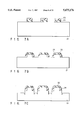
- FIGS. 1A and 1B show a method for implanting an impurity by an ion implantation into an element region by prior art.
- FIG. 1A shows a plan pattern of a MOS transistor. An element region 102 is isolated by an isolation region 103. A gate electrode 104 is formed on the element region 102. In this transistor, a resist pattern 105 is formed only on an unnecessary portion, and an impurity such as, for example arsenic or the like is implanted into the element region by using the resist pattern 105 and the gate electrode 104 as masks.
- FIG. 1B is a cross-sectional view taken along the line IB--IB of FIG. 1A.
- a trench is formed in the element isolation region 103 of the substrate 101, and the trench is filled with SiO 2 .
- the gate electrode 104 is formed on the element region 102, and a portion where an ion implantation is not desired is covered with the resist pattern 105 in this state.
- the arsenic is implanted in the entire element region 102, and an impurity region 106 is formed in the element region 102 of the substrate 101.
- a stress received by the isolation region 103 is concentrated at a corner 107 of the element region 102. Further, a primary defect due to the ion implantation is grown to a large defect due to a dislocation by the concentrated stress, and a problem of an increase of a junction leakage current occurs.
- FIG. 2 is a plan view of a DRAM cell of a conventional structure
- FIG. 3 is a sectional view taken along the line III--III.
- reference numeral 801 denotes a gate wiring (word line); 802, a bit line, 803; a contact between A1 gates; 805, a bit line contact; and 806, a capacitor contact.
- Reference numeral 804 denotes an element region; and 807, a storage note of a lower electrode of the capacitor.
- a P-type well 812 is provided on a silicon substrate 817, and an isolation region 810 in which an insulator is embedded in a trench is formed in the P-type well 812.
- a gate oxide film 813 is formed on the P-type well 812 isolated by the isolation region 810, and a gate wiring 801 is formed on the gate oxide film 813 and the isolation region 810.
- the bit line 802 is formed on the gate wiring 810 through an interlayer insulating film 816, and an A1 wiring 809 is disposed further on the bit 802 through the interlayer insulating film 816', a capacitor insulating film 819 and an interlayer insulating film 811.
- the A1 wiring 809 is connected to the gate wiring 801 through the contact 803 between the A1 gates.
- a crystal defect 814 is extended from the corner of the element isolation region 810 into the P-type well 812.
- the trench isolating method when intended to be applied to a fine semiconductor element, there is a trend of deteriorating a junction leakage current characteristics of the device due to generation of the crystal defect. Further, the stress is concentrated particularly at the corner of the element region even by the ion implantation, thereby generating the crystal defect, and an increase in the junction leakage current is introduced.
- An object of the present invention is to provide a semiconductor device which can prevent a crystal defect due to such a trench isolation, an impurity implantation.
- Another object of the present invention is to provide a method for manufacturing such a semiconductor device.
- a semiconductor device comprising a semiconductor substrate having a groove, and a semiconductor element formed in a surface region of this semiconductor substrate, wherein a substance having a thermal expansion coefficient different from the semiconductor substrate is embedded at least in a part of the groove, a crystal defect is generated in the semiconductor substrate from the groove, thereby a strain of the surface area of the semiconductor substrate is sufficiently alleviated, and a crystal defect is not generated in a region necessary for a circuit operation of the semiconductor element.
- a semiconductor device comprising a semiconductor substrate, and a semiconductor element formed in an element region of the semiconductor substrate, wherein at least one of corners of the element region or at least one of ends of a region of the element underlying a gate electrode thereof region has an impurity concentration lower than a portion except those of the element region.
- a semiconductor device comprising a semiconductor substrate, a MIS type semiconductor element formed in a surface region of the semiconductor substrate, a first wiring layer for forming or connected to a gate electrode of the MIS type semiconductor element, and a second wiring layer disposed above the first wiring layer, wherein a defect concentrated region exists in the semiconductor substrate under a connecting portion of the first and second wiring layers.
- a semiconductor device comprising a semiconductor substrate having a groove, an element isolation region having an insulating film embedded in the groove of the semiconductor substrate, an element region formed of a plurality of low concentration regions isolated by the element isolation region, semiconductor elements respectively formed on the plurality of low concentration regions, and a high concentration impurity region surrounding a periphery of the element region for attracting metal impurity in the semiconductor substrate.
- FIGS. 1A and 1B are a plan view and a sectional view showing a disposing example of a conventional resist pattern and a state of an ion implantation;
- FIG. 2 is a plan view showing a portion of a conventional DRAM cell array
- FIG. 3 is a sectional view taken along the line III--III of FIG. 12;
- FIG. 4 is a sectional view of a semiconductor device according to a first embodiment of the present invention.
- FIG. 5 is a sectional view of a semiconductor device in which the first embodiment of the present invention is applied to a CMOS;
- FIGS. 6A to 6H are sectional views showing manufacturing steps of a semiconductor device according to the first embodiment of the present invention.
- FIGS. 7A to 7I are sectional views showing manufacturing steps of a semiconductor device according to a second embodiment of the present invention.
- FIGS. 8A to 8I are sectional views showing manufacturing steps of a semiconductor device according to a third embodiment of the present invention.
- FIGS. 9A to 9I are sectional views showing manufacturing steps of a semiconductor device according to a fourth embodiment of the present invention.
- FIGS. 10 to 10I are sectional views showing manufacturing steps of a semiconductor device according to a fifth embodiment of the present invention.
- FIGS. 11A and 11B are a plan view and a sectional view of a semiconductor device according to a sixth embodiment of the present invention.
- FIGS. 12 to 16 are plan views showing various disposing examples of a resist pattern to be used for the sixth embodiment of the present invention.
- FIG. 17 is a plan view showing a semiconductor device according to a seventh embodiment of the present invention.
- FIG. 18 is a sectional view taken along the line XVIII--XVIII of FIG. 17;
- FIG. 19 is a sectional view taken along the line XIX--XIX of FIG. 17;
- FIG. 20 is a sectional view showing a semiconductor device according to an eighth embodiment of the present invention.
- FIG. 21 is a sectional view showing a semiconductor device according to a ninth embodiment of the present invention.
- FIG. 22 is a sectional view showing a semiconductor device according to tenth embodiment of the present invention.
- FIG. 23 is a plan view showing a portion of a DRAM cell array according to an eleventh embodiment of the present invention.
- FIG. 24 is a sectional view taken along the line XXIV--XXIV of FIG. 23;
- FIGS. 25A and 25B are a plan view and a sectional view showing a main portion of a configuration of a CMOS integrated circuit according to twelfth embodiment of the present invention.
- FIGS. 26A to 26E are sectional views showing a manufacturing process of a CMOS integrated circuit according to the twelfth embodiment of the present invention.
- FIGS. 27A and 27B are schematic structural views of a MOS memory according to a modified example of the twelfth embodiment of the present invention.
- a groove deeper than a surface region of the semiconductor device is formed in a semiconductor substrate formed with a semiconductor element on the surface region, and a substance having a thermal expansion coefficient different from said semiconductor substrate is embedded in at least a part of the groove. Therefore, a crystal defect is generated from the groove in the semiconductor substrate, thereby sufficiently alleviating a strain of the surface region of the semiconductor substrate, and no crystal defect is generated in a region necessary for a circuit operation of the semiconductor element formed in the surface region.
- a semiconductor layer having a second groove is formed on a semiconductor substrate having a first groove.
- the first groove is embedded with a first substance
- the second groove is embedded with a second substance.
- the first substance has a thermal expansion coefficient different from the semiconductor substrate, and the first and second substances are so selected that a difference between the thermal expansion coefficients of the second substance and the semiconductor layer is smaller than a difference between the thermal expansion coefficients of the first substance and the semiconductor substrate.
- a crystal defect is generated from the first groove in the semiconductor substrate, thereby sufficiently alleviating a strain of the semiconductor layer, and a crystal defect is not generated in a region necessary for a circuit operation of the semiconductor element formed in the semiconductor layer.
- the semiconductor elements to be formed can be formed in a structure to be electrically isolated by the second groove and the second substance embedded in the second groove.
- the semiconductor layer formed on the semiconductor substrate can be epitaxially grown on the semiconductor substrate, and its film thickness is preferably larger than a width of a depletion layer to be formed at a p-n junction of the element.
- Such a semiconductor device can be manufactured by the following method.
- This method comprises the steps of forming a first groove on a semiconductor substrate, embedding a first substance having a thermal expansion coefficient different from said semiconductor substrate in the first groove, epitaxially growing a semiconductor layer on said semiconductor substrate, forming a second groove in said semiconductor layer, embedding a second substance in the second groove, and forming a semiconductor element in said semiconductor layer.
- a plurality of grooves embedded with insulating materials are formed in a semiconductor substrate, a semiconductor element is formed in an element region isolated by the first grooves, and a second groove embedded with an insulating material is formed in a bottom of the first groove.
- a crystal defect is generated from the second groove in the semiconductor substrate, thereby sufficiently alleviating a strain of the element region, and a crystal defect is not generated in a region necessary for a circuit operation of the semiconductor element formed in the element region.
- a ratio b/a of a total depth b of the first and second grooves to an interval a between adjacent second grooves is preferably 1/2 or more.
- a crystal defect generated from the first groove of the semiconductor device is terminated at the bottom
- Impurities of different conductivity type can be introduced into the semiconductor substrate to form two well regions.
- an isolation between wells can be conducted by the first groove or by both the first and second grooves.
- the semiconductor device of the structure in the above paragraph (2) is manufactured by the method comprising the steps of forming a second groove in a semiconductor substrate, forming a first groove narrower than the second groove in a bottom of the second groove, embedding the first and second grooves with insulating materials, and forming a semiconductor element in an element region isolated by the second groove.
- the crystal defect is previously generated in the semiconductor substrate or in a deep portion of the semiconductor substrate, thereby alleviating a strain of the semiconductor layer or the surface region of the semiconductor substrate, with the result that an element can be formed in a defect free state. Therefore, the semiconductor element formed in the semiconductor layer or the surface area of the semiconductor substrate can be reduced in a junction leakage current due to the crystal defect.
- the groove having a large aspect ratio which has been heretofore difficult to form can be formed in two stages, an isolation between wells can be relatively simply conducted.
- a corner of the element region or an end of the element region to be superposed on a gate electrode has a lower impurity concentration than a portion except the corner or end portion of the element region. More specifically, an impurity implantation is conducted in the state that a resist pattern for implanting an impurity covers a corner of the element region or an end of the element region to be superposed on the gate electrode.
- a defect concentrated region exists in the portion of the semiconductor substrate under a connecting portion of a first wiring layer constituting a gate electrode of a MOS semiconductor element to a second wiring layer disposed above the first wiring layer.
- the defect concentrated region is arranged in the portion of the semiconductor substrate under a connecting portion between the wirings stereoscopically crossing on an Si substrate, an increase of an area due to the provision of the defect concentrated region is small, and a decrease of an area of the element region does not occur. Because, the portion of the substrate under the connecting portion between the wirings is not originally frequently formed with a device.
- a groove deeper than a well is formed in a portion of a semiconductor substrate under a connecting portion of the first and second wiring layers, and a crystal defect is generated from a bottom of the groove.
- a defect concentration region can be formed without increasing an area. Further, since the groove deeper than the element region is formed and the defect is concentrated at its bottom, a distance between the crystal defect and the element can be increased.
- a high concentration impurity region is formed in a semiconductor substrate under a connecting portion of the first and second wiring layer, and a crystal defect is generated from a bottom of the impurity layer.
- a defect concentrated region can be formed without increasing its area, and a defect in the element region can be reduced.
- a groove in which a groove width is abruptly changed and which is deeper than a well having at least one corner (an angular portion) of a plane pattern shape is formed in a portion of a semiconductor substrate under a connecting portion of first and second wiring layers, and a crystal defect is generated from the corner.
- a defect concentrated region can be formed without increasing its area, and a defect in the element region can be reduced.
- a defect concentrated layer for gettering (sucking) the crystal defect is arranged apart from the element region, the defect is scarcely generated in the element region, and the defect generated in the element region and a metal contamination are removed. After a large defect such as a dislocation occurs in the defect concentrated layer, a defect free of the element region is maintained even if later steps are executed. Therefore, device characteristics such as junction leakage current characteristics, gate oxide film reliability are remarkably improved. Since the above-described defect concentrated layer is disposed in a region in which a device such as a MOSFET or the like is not normally formed (a region not utilized for a MOSFET due to specific reason), an increase of the area of the device is not introduced. That is, a vacant space can be effectively utilized as a gettering sink.
- a high concentration impurity region for drawing metal impurity in a semiconductor substrate is provided around a periphery of an element region having a plurality of low concentration regions isolated by element isolation region.
- the semiconductor device comprises an element region having semiconductor elements each having a low concentration impurity region of 3 ⁇ 10 15 cm -2 or less, regularly disposed and electrically isolated by element isolation region obtained by embedding an insulating film in a groove formed in a semiconductor substrate, and a high concentration impurity region provided on an outer periphery of the element region and having 5 ⁇ 10 15 cm -2 or more for drawing metal impurity in the element region.
- a stress strain due to an insulting film can be alleviated. Therefore, a crystal defect can scarcely occur in the element region, and the metal impurity can be forcibly drawn out of the element region into the defect.
- FIG. 4 is a sectional view showing a semiconductor device according to a first embodiment of the present invention.
- a first groove 2 is formed in a semiconductor substrate 1, and a first embedding material 3 is embedded in the first groove 2.
- the first embedding material 3 has a thermal expansion coefficient different from the semiconductor substrate, thereby generating a stress at the first groove.
- a semiconductor layer 4 is formed on the semiconductor substrate 1.
- the semiconductor layer 4 constitutes an element forming region, and two element forming regions in the semiconductor layer 4 are electrically isolated by a substance 6 as a second embedding material embedded in a second groove 5.
- a gate oxide film 7 is formed on the semiconductor layer 4, and a gate electrode 8, a source electrode 9 and a drain electrode 10 are provided. Further, an interlayer insulting film 11 is deposited, a metal wiring layer 13 is formed on the interlayer insulating film 11, and connected to the gate electrode 8, the source electrode 9 and the drain electrode 10 via a contact hole 12.
- an embedding material having a tensile stress may be embedded in the first groove, or an embedding material having a reverse compressive stress may be embedded in the first groove.
- a crystal defect is generated from a bottom of the first groove by a large stress. If the crystal defect is once generated, i.e., a dislocation once occurs, the stress in the other region is then alleviated, and a strain is reduced. Therefore, a crystal defect due to the stress is not almost generated in the semiconductor layer 4 formed on the semiconductor substrate having the first groove.
- FIG. 5 shows an example of the present invention applied to a CMOS.
- an isolation of an n-type well 14 from a p-type well 15 is conducted with a first groove and a second groove.
- This structure has an advantage that there is no necessity of forming a groove having a large aspect ratio which has been difficult by present technique. Further, a "retrograde well" can be realized by a conventional apparatus without using a high acceleration energy ion implanting unit.
- FIG. 1 One example of a method for manufacturing a semiconductor device shown in FIG. 1 will be described with reference to FIGS. 6A to 6H.
- a mask material 16 is deposited on a semiconductor substrate 1, only a first groove forming region is opened, and the other portion is covered with the mask material 16 (FIG. 6A).
- the mask material 16 used at this time may not always be resist, but a silicon oxide film deposited and patterned may be employed.
- a silicon substrate is etched by using the mask to form a first groove 2. This etching generally uses an RIE to provide anisotropy (FIG. 6B).
- the mask material is removed, and the first embedding material 3 is deposited on the entire substrate (FIG. 6C).
- the first embedding material 3 is necessary to have a thermal expansion coefficient different from the semiconductor substrate 1.
- the silicon substrate when a silicon nitride film may be deposited by using an LPCVD, the silicon nitride film has largely different thermal expansion coefficient from silicon (a tensile stress of a magnitude of 1 ⁇ 10 10 dyne/cm 2 is generated.), and hence it is convenient for the present invention.
- the first embedding material 3 is removed except a portion of the groove. This can be realized by masking it by a resist pattern 17 and then using an etching-back step by an RIE (FIG. 6D).
- a heating is carried out, thereby generating a crystal defect (dislocation) from the bottom of the first groove 2. It is necessary to determined a depth and an interval of the first grooves so that a defect (a dislocation) generated at this time does not arrive at a substrate surface. For example, in the case of a silicon substrate of a plane (100), when a section is taken in parallel with a plane (011), a dislocation is inclined to occur in a direction in parallel with a plane (111), and hence the dislocation occurs in a direction of about 54.74° from a horizontal plane.
- a depth of the groove is larger by at least ⁇ 2 times than an interval of the groove in order that the dislocation may not arrive at a semiconductor substrate surface.
- the dislocation is terminated at the side face of the opposed groove, and hence a strain of the substrate is preferably alleviated.
- boron is ion implanted to form a p-type well (FIG. 6E).
- the semiconductor layer 4 is formed on the semiconductor substrate 1.
- the semiconductor layer 4 must be formed while holding crystallinity under the conditions of epitaxially growing on a base substrate since the semiconductor element is formed in the semiconductor layer (FIG. 6F)
- the semiconductor layer is formed by a silicon molecular beam epitaxy method or an organometallic molecular CVD (MOCVD).
- a thickness of the semiconductor layer 4 is limited to such a thickness that a stress generated from the second groove 5 to be used for element isolation is sufficiently reduced.
- the thickness must be larger than a width of the depletion layer formed at the p-n junction of the element. The reason is because, when the depletion layer is crossed by the crystal defect, it might become a cause of generating a junction leakage current. If the defect can be retained only in the bottom of the semiconductor substrate, the thickness of the semiconductor layer is reduced as much as possible, and a dose to the semiconductor layer is suppressed to improve performance of the element.
- a second groove 5 is formed as an element isolation region in the semiconductor layer.
- This second groove 5 is formed by providing a mask having a pattern for an element isolation region similarly to the first groove 2 on the semiconductor layer 4, and processing it using the mask by an RIE or the like. In this case, there is no problem even if the second groove 5 is superposed on the first groove 2. Further, when the second embedding material 6 is deposited thereon, and an element isolation region is formed by an RIE etching-back method (FIG. 6G).
- the embedding material 6 of this case is required for a thermal expansion coefficient not largely different from that of the semiconductor layer unlike the material 3 embedded in the first groove 2.
- a material such as silicon oxide and polysilicon are used.
- a depositing temperature is important. When it is deposited at about 650° to 750° C., it is known that only a low compressive stress of 0 to 1 ⁇ 10 9 dyne/cm 2 is generated. Further, it is known that a tensile stress of about 1 to 4 ⁇ 10 9 dyne/cm 2 is generated at a low temperature of 400° to 500° C. In either case, the silicon oxide film generates a stress smaller than the silicon nitride film. Thus, the material 6 embedded in the second groove 5 can make the semiconductor layer defect free.
- a gate electrode material such as, for example, polysilicon is deposited.
- the polysilicon film is patterned to form a gate electrode using an RIE or the like.
- an impurity is ion implanted into the semiconductor layer 4 to form a source region 9 and a drain region 10 (FIG. 6H).
- arsenic is used as an impurity.
- the gate electrode 8 may be processed after an impurity is previously doped.
- An interlayer insulating film 11 is eventually deposited, a contact hole 12 is opened, and a metal wiring 13 is formed, thereby completing a semiconductor device shown in FIG. 4.
- a CMOS as shown in FIG. 5 can be similarly manufactured. That is, if implantation of the impurities into one region is performed while masking another region in the case of forming the wells, the CMOS device can be manufactured by the similar steps.
- FIGS. 7A to 7I are sectional views showing manufacturing steps of a semiconductor device according to a second embodiment of the present invention.
- a thermal oxide film 22 of a thickness of 200 nm is formed on a surface of a p-type silicon substrate 21
- a resist pattern 23 is formed on an element forming region, and with the resist pattern 23 used as a mask
- the thermal oxide film 22 is etched by an RIE method (FIG. 7A).
- the resist pattern 23 is removed, and with the thermal oxide film 22 used as a mask, the silicon substrate 21 is etched in a depth of, for example, 1 ⁇ m by an RIE method to form a first groove.
- a protruding insular portion is formed.
- a first silicon oxide film 24 is deposited on an entire surface in a thickness of about 100 nm by a CVD method, the entire surface is etched by the RIE. At this time, the first silicon oxide film 24 remains on a sidewall of the first groove (FIG. 7B).
- the silicon substrate 21 is etched in a depth of 1 ⁇ m under the conditions of power of 300 W or less and pressure of 75 mTorr by an RIE method using only HBr gas, thereby forming a second groove.
- the second groove is dug at a base of the sidewall at a sharp angle (FIG. 7C). With such a shape, a crystal defect is feasibly generated from the portion.
- the thermal oxide film 22 and the first silicon oxide film 24 are removed by fluoric acid series aqueous solution such as NH 4 F aqueous solution.
- the second silicon oxide film 25 is deposited in a thickness of 2.4 ⁇ m by a CVD method.
- a second resist pattern 26 of a thickness of 2.0 ⁇ m is formed on a wide element isolation region, then coated with third resist 27 having low viscosity, thereby flattening an uneven portion of the surface. (FIG. 7D).
- the second and third resists 26, 27 and the second silicon oxide film 25 are etched back under the conditions that etching rates of the second and third resists 26, 27 and the second silicon oxide film 25 become equal by an RIE.
- the silicon oxide film 25 of 50 nm is retained on the insular portion. Thereafter, it is etched by 50 nm with NH 4 F aqueous solution (FIG. 7E).
- boron ions are implanted in the entire silicon substrate 21 by an accelerating voltage of 50 keV and a dose of 6 ⁇ 10 12 cm -2 , thereby forming a p-type well region 28 (FIG. 7F). Thereafter, it is heat treated at 1000° C. for 20 sec. in a nitrogen atmosphere by using a rapid thermal annealing method (RTA), thereby activating boron ions.
- RTA rapid thermal annealing method
- a polycrystalline silicon film 30 of a thickness of 200 nm is deposited on an entire surface, and then arsenic ions are implanted in a polycrystalline silicon film 30 at an accelerating voltage of 30 Key and a dose of 5 ⁇ 10 15 cm -2 . Thereafter, it is heat treated at 1,000° C. for 20 sec. in a nitrogen atmosphere by using the RTA, thereby activating the arsenic ions (FIG. 7G). Then, with the resist pattern (not shown) used as a mask, the polycrystalline silicon film 30 is etched by the RIE, and a gate electrode 32 is formed (FIG. 7H).
- N-type impurity is ion implanted according to manufacturing steps of an ordinary N-type MOSFET using the gate electrode 32 as a mask, thereby forming a diffused region 33. Further, a CVD oxide film 34 passivating step, a contact hole opening step and an A1 wiring 35 forming step are conducted, thereby completing an N-type MOSFET (FIG. 7I).
- the crystal defect is generated from the bottom of the second groove, the generated crystal defect 36 is terminated at the bottom of the second groove or the bottom of the adjacent second groove, not extended to the element region, but the element is resultantly defect-free state.
- the N-type MOSFET is used as the example.
- this embodiment can also be applied similarly to a CMOS, a P-type MOSFET.
- FIGS. 8A to 8I are sectional views showing manufacturing steps of an N-type MOSFET according to a third embodiment of the present invention.
- a thermal oxide film 42 of a thickness of 200 nm is formed on a surface of a p-type silicon substrate 41, a resist pattern 43 is formed on an element forming region, and with the resist pattern 43 used as a mask, the thermal oxide film 42 is etched by an IRE method (FIG. 8A).
- the resist pattern 43 is removed, with the thermal oxide film 42 used as a mask, the silicon substrate 41 is etched in a depth of 1 ⁇ m by an IRE method, thereby forming a first groove.
- a protruding insular portion is formed.
- the second resist pattern 44 is formed at a position deviating from that of the resist pattern 43 (FIG. 8B).
- the silicon substrate 41 is etched in a depth of 1 ⁇ m by an IRE method, thereby forming a second groove (FIG. 8C).
- a second groove of a narrow width and a deep depth is formed, and hence a crystal defect is easily generated from the bottom of the groove.
- a silicon oxide film 45 of a thickness of 2.4 ⁇ m is deposited by a CVD method.
- a third resist pattern 46 of a thickness of 2 ⁇ m is formed on a wide element isolation region of the silicon oxide film 45, then coated with a fourth resist 47 having low viscosity, thereby flattening an uneven portion of the surface (FIG. 8D).
- the third and fourth resists 46, 47 and a silicon oxide film 45 are etched back under the conditions that etching rates of the third and fourth resists 46, 47 and the silicon oxide film 45 become equal by an RIE.
- a silicon oxide film 45 of 50 nm is retained on the insular portion.
- the entire surface is etched by 50 nm with NH 4 F aqueous solution FIG. 8E).
- boron ions are implanted in the silicon substrate 41 at an accelerating voltage of 60 keV and dose of 6 ⁇ 10 12 cm -2 , thereby forming a p-type well region 48 (FIG. 8F). Thereafter, it is heat treated at 1,000° C. for 20 sec. in a nitrogen atmosphere by using a rapid thermal annealing method (RTA), thereby activating boron ions.
- RTA rapid thermal annealing method
- a polycrystalline silicon film 50 of a thickness of 200 nm is deposited on the entire surface, and then arsenic ions are implanted in the polycrystalline silicon film 30 at an accelerating voltage of 30 keV and dose of 5 ⁇ 10 15 cm -2 . Thereafter, it is heat treated at 1,000° C. for 20 sec. in a nitrogen atmosphere by using the RTA, thereby activating the arsenic ions (FIG. 8G). Then, with the resist pattern (not shown) used as a mask, the polycrystalline silicon film 50 is etched by an RIE, thereby forming a gate electrode 52 (FIG. 8H).
- N-type impurity is ion implanted according to manufacturing steps of an ordinary N-type MOSFET, a diffused region 53 is formed, and further a CVD oxide film 54 passivating step, a contact hole opening step and an A1 wiring 55 forming step are conducted, thereby completing an N-type MOSFET (FIG. 8I).
- the crystal defect is generated from the bottom of the second groove, the generated crystal defect 56 is terminated at the bottom of the second groove or the bottom of the adjacent second groove, not extended to the element region, but the element region is resultantly defect-free state.
- the N-type MOSFET is used as the example.
- the embodiment can be similarly applied to a CMOS, a P-type MOSFET.
- FIGS. 9A to 9I are sectional views showing manufacturing steps of an N-type MOSFET according to a fourth embodiment of the present invention.
- a first thermal oxide film 62 of a thickness of 200 nm is formed on a surface of a p-type silicon substrate 61, then a resist pattern 63 is formed on an element forming region, and with the resist pattern 63 used as a mask, the first thermal oxide film 62 is etched by an RIE method (FIG. 9A).
- the resist pattern 63 is removed, and with the first thermal oxide film 62 used as a mask, the silicon substrate 61 is etched in a depth of 2 ⁇ m by an RIE method to form a groove. Thus, a protruding insular portion is formed. Then, after the thermal oxide film 62 is removed with NH 4 F aqueous solution, and a second thermal oxide film 64 is formed on the entire surface of the substrate 61 by using oxidizing conditions to permit a facet to be present in the bottom of the groove (FIG. 9B). Incidentally, when the facet appears at the bottom of the groove, a crystal defect is easily generated from the facet.
- the polysilicon film 65 of a thickness of 2.4 ⁇ m is deposited by a CVD method, and etched back by using a CDE method. At this time, after the silicon oxide film 65 is deposited, it is flattened with the resist, and may be etched back under the condition that etching rates of the polysilicon film and the resist become equal by RIE.
- the second resist pattern 66 is formed, and with the second resist pattern 66 used as a mask, it is etched in a depth of 1 ⁇ m under the condition that etching rates of the silicon substance 61 and the first polycrystalline silicon 65 become equal (FIG. 9C). Then, the second resist pattern 66 is removed.
- the silicon oxide film 67 is deposited in a thickness of 1.4 ⁇ m by a CVD method. Further, a third resist pattern 68 of a thickness of 1.4 ⁇ m is formed on a wide element isolation region, and the coated with a fourth resist 69 having low viscosity, thereby flattening an uneven surface (FIG. 9D).
- the third and fourth resists 68, 69 and a silicon oxide film 67 are etched back under the condition that etching rates of the third and fourth resists 68, 69 and the silicon oxide film 67 become equal by an IRE.
- the silicon oxide film 67 of 50 nm is retained on the insular portion. Thereafter, it is etched by 50 nm with NH 4 F aqueous solution (FIG. 9E).
- boron ions are implanted in the entire silicon substrate 61 at an accelerating voltage of 60 key and dose of 6 ⁇ 10 12 cm -2 , thereby forming a p-type well 70. Thereafter, it is heat treated at 1,000° C. for 20 sec in a nitrogen atmosphere by using a rapid thermal annealing method (RTA), thereby activating the boron ions.
- RTA rapid thermal annealing method
- the dummy oxide film 71' is removed with NH 4 F aqueous solution, and a gate oxide film 71 of a thickness of 10 nm is newly formed (FIG. 9F).
- a second polycrystalline silicon film 72 of a thickness of 200 nm is deposited on the entire surface, and then arsenic ions are implanted in the polycrystalline silicon film 72 at an accelerating voltage of 30 keV and dose of 5 ⁇ 10 15 cm -2 . Then, it is heat treated at 1,000° for 20 sec. in a nitrogen atmosphere by using an RTA, thereby activating the arsenic ions (FIG. 9G). Subsequently, with the resist pattern (not shown) used as a mask, the polycrystalline silicon film 72 is etched by an RIE, thereby forming a gate electrode 74 (FIG. 9H).
- N-type impurity ions are implanted, a diffused region 75 is formed, and further a passivating step for CVD oxide film 76, a contact hole opening step and an A1 wiring 77 forming step are executed, thereby completing an N-type MOSFET (FIG. 9I).
- the crystal defect is generated from the bottom of the second groove, the generated crystal defect 78 is terminated at the bottom of the second groove or the bottom of the adjacent second groove, not extended to the element region, but the element region is in a crystal defect free state.
- the N-type MOSFET is used as the example.
- this embodiment may be similarly applied to a CMOS, a P-type MOSFET.
- FIGS. 10A to 10I are sectional views showing manufacturing steps of a semiconductor device according to a fifth embodiment of the present invention.
- a thermal oxide film 82 of a thickness of 200 nm is formed on the surface of a p-type silicon substrate 81, a resist pattern 83 is formed on an element forming region, and with the resist pattern 83 used as a mask, the thermal oxide film 82 is etched by an RIE method (FIG. 10A).
- the resist pattern 83 is removed, and with the thermal oxide film 82 used as a mask, the silicon substrate 81 is etched in a depth of 1 ⁇ m by an RIE method, thereby forming a first groove. Thus, a protruding insular portion is formed. Then, a first silicon oxide film 84 of a thickness of 100 nm is deposited on the entire surface by a CVD method, and then the entire surface is etched by an RIE. At this time, the first silicon oxide film 84 is retained on a sidewall of the first groove (FIG. 10B).
- the silicon substrate 81 is etched in a depth of 1 ⁇ m by an RIE method using only HBr gas under the conditions of power of 300 W or less and a pressure of 75 mTorr, thereby forming a second groove.
- the second groove is dug at a base of the sidewall in a sharp angle state (FIG. 10C). With such a shape, the crystal defect is easily generated from the portion.
- the thermal oxide film 82 and the first silicon oxide film 84 are removed with NH 4 F aqueous solution.
- the second silicon oxide film 85 of a thickness of 2.4 ⁇ m is deposited by a CVD method.
- a second resist pattern 86 of a thickness of 2.0 ⁇ m is formed on a wide element isolation region, and then coated with a third resist 87 having low viscosity, thereby flattening an uneven portion of the surface (FIG. 10D).
- boron ions are implanted in the entire silicon substrate 81 at an accelerating voltage of 60 keV and dose of 6 ⁇ 10 12 cm 31 2, thereby forming a p-type well region 88. Thereafter, it is heat treated at 1,000° C. for 20 sec. in a nitrogen atmosphere by using a rapid thermal annealing method (RTA), thereby activating the boron ions.
- RTA rapid thermal annealing method
- an impurity is implanted by using a high accelerating ion implanting method.
- the implantation of the impurity is not limited to this stage.
- the impurity may be partly implanted. In this case, the case where the impurity is implanted in the entire surface will be described.
- the impurity is implanted in a depth of the same degree as the depth of the second groove or deeper depth than the depth of the second groove in the entire surface by using a high speed ion implanting method, thereby forming a damage layer 89.
- the damage layer 89 is formed to terminate a crystal defect generated from the second groove (FIG. 10F).
- the dummy oxide film 90' is removed with NH 4 F aqueous solution, and a gate oxide film 90 of a thickness of 10 nm is newly formed.
- a polycrystalline silicon film 91 of a thickness of 200 nm is deposited on the entire surface, and then arsenic ions are implanted in the polycrystalline silicon film 91 at an accelerating voltage of 30 keV and dose of 5 ⁇ 10 15 cm 31 2. Thereafter, it is heat treated at 1,000° C. for 20 sec. in a nitrogen atmosphere by using an RTA, thereby activating the arsenic ions (FIG. 10G).
- the polycrystalline silicon film 91 is etched by an RIE, thereby forming a gate electrode 92 (FIG. 10H).
- a gate electrode 92 (FIG. 10H).
- N-type impurity ions are implanted, thereby forming a diffused layer 93, and further a CVD oxide film 94 passivating step, a contact hole opening step and an A1 wiring 95 forming step are conducted, thereby completing an N-type MOSFET (FIG. 10I).
- the crystal defect is generated from the bottom of the second groove, the crystal defect 97 generated is terminated at the damage layer 89, the bottom of the second groove, or the bottom of the adjacent second groove, not extended to the element region, but the element region is resultantly in a free state.
- the N-type MOSFET is used as the example.
- this embodiment may be similarly applied to a CMOS, a P-type MOSFET.
- the crystal defect is previously generated in the deep portion of the semiconductor device using the trench isolation method, the element can be formed at the upper portion of the semiconductor substrate or the semiconductor layer in a defect free state in the state that the strain in the substrate is alleviated. Therefore, the junction leakage current due to the crystal defect can be reduced.
- This embodiment shows various examples of preventing a crystal defect according to a pattern shape of a resist pattern.
- a resist pattern in which a shape of an opening is of an octagonal shape is used.
- an element region 202 is isolated by an element isolation region 203, then a gate electrode 204 and the like is formed if necessary, and a resist pattern 205 for implanting an impurity is formed by using a photolithographic step.
- the resist pattern 205 is formed in a shape for covering a corner 206 of the element region.
- a resist pattern 303 to become a mask at the time of ion implanting covers a corner 304 of the element region 302, thereby suppressing generation of a large crystal defect of ion implantation.
- the resist pattern 303 having a corner with only 90° may be used.
- an element region 402 of a complicated shape isolated by an element isolation region 401 is formed.
- a corner 405 of an element region in which a crystal defect is not possibly generated or may be generated without trouble is not covered with a resist 403, but a corner 404 of the element region 402 in which the crystal defect might be generated but is undesired to be generated is covered with the resist pattern 403.
- the resist pattern 403. it is not necessary to cover all the corners of the element regions 402 with the resist patterns 403.
- the case of a trench element isolation has been described.
- an ordinary LOCOS method and the other element isolating method are used, similar effect can be obtained.
- the resist pattern is used as the mask, and the impurity is implanted by the ion implantation.
- the similar effect can also be obtained even by implanting the impurity with an oxide film used as a mask by a solid phase or vapor phase diffusion or with a corner used as a mask by other method.
- an end 605 of a region in which an element region 602 and a gate electrode 603 are superposed is also covered with a resist pattern 604. This is because a stress is concentrated also at the end 605 of the region in which the element region 602 and the gate electrode 603 are superposed, and thus the similar effect to that of the above-described example can be obtained.
- a resist pattern 703 having an opening of the same shape as a element region 702 and altered at a position to so dispose as to cover a corner 74 of the region 702 is shown.
- the shape of the resist pattern is so selected that the corner of the element region in which the stress is concentrated and the portion in which the impurity is implanted are not superposed. Therefore, a large dislocation can be prevented, thereby reducing the junction leakage current due to the crystal defect.
- FIG. 17 is a plan view showing a portion of a DRAM (dynamic random access memory) cell array using a stack type capacitor according to a seventh embodiment of the present invention
- FIG. 18 is a sectional view taken along the line XVIII--XVIII of FIG. 17
- FIG. 19 is a sectional view taken along the line XIX--XIX of FIG. 17.
- FIGS. 18 and 19 are sectional views showing the case where the manufacturing steps are advanced till the formation of an initial metal wiring .(first A1).
- a metal wiring (A1 in this example) 809 having substantially the same width as that of a gate wiring and extending in the same direction as that of the gate wiring directly above the gate wiring is formed, and contacts 803 for connecting in places the metal wiring 809 to the gate electrode 801 is formed.
- a region provided with the contact is called "an A1 shunt region 820"
- an interval between the A1 shunt region 820 and another A1 shunt region ranges several tens to hundred and several tens of micron in a DRAM of a gigabit level.
- FIGS. 17 to 19 illustrate a method for inducing a defect by forming a deep groove 808' in the region 808.
- a crystal defect 814 in which a corner of a bottom of a groove is used as an end point (starting point) 814' is easily generated.
- the other end point (ending point) may position at a corner of a bottom of the other groove, or a high strain layer (e.g., a high concentration impurity layer 815) formed in the same depth or deeper than the bottom of the groove may be formed in the substrate of a cell array region.
- the drawings illustrate the latter. If the crystal defect is generated only at the bottom of the groove and not extended to the element region, the high concentration impurity layer 815 may not be present.
- a method for manufacturing a semiconductor device according to the seventh embodiment will be simply explained.
- an Si wafer 817 of a surface orientation (100) is prepared, and a high concentration impurity region 815 is formed at a position of a depth of, for example, about 5 ⁇ m from a surface of the wafer 817 by a high acceleration ion implantation or solid-phase diffusion and epitaxial growth.
- a groove 808' of the depth of the same degree is formed, and embedded with an SiO 2 insulator.
- boron is ion implanted and thermally diffused to form a P-type well 812 of a depth of 2-3 ⁇ m.
- a patterning by a lithography is executed, a shallow groove 810 of a depth of about 0.5 ⁇ m is formed, the groove 810 is embedded with SiO 2 insulator, thereby flattening the surface.
- a plane pattern shape of the element active region 804 is designed obliquely to a gate wiring 801.
- a trench isolation is employed as an element isolation method.
- a LOCOS method may be employed.
- a gate oxide film 813 of a thickness of about 6 nm is formed by a thermal oxidation, a polysilicon of a thickness of 150 nm is further deposited, an impurity is doped, and WSi (tungsten silicide) is sputtered. Then, the polysilicon layer and the WSi layer are patterned by a lithography and an IRE, thereby forming a gate wiring 801.
- an SiO 2 film 816 is deposited as an interlayer insulating film in a thickness of about 300 nm by a CVD method, and flattened by a CMP (chemical mechanical polishing).
- a bit line contact hole 805 is formed in the interlayer insulating film 816, polysilicon is deposited in a thickness of about 350 nm, ion implanted and etched back by an RIE, thereby embedding the polysilicon in the contact hole 805.
- the doped polysilicon and WSi are respectively formed in thicknesses 50 and 150 nm, forming a bit line 802 by patterning.
- frequency, a contact hole 803' of an A1 shunt portion and an a plug 802' due to the bit line are simultaneously formed.
- an aspect ratio of the contact may be conveniently small.
- an SiO 2 film 816' is deposited as an interlayer insulting film in a thickness of about 300 nm by a CVD method, and flattened. Then, a capacitor contact 806 is opened, and a lower electrode (storage node: 807) is formed, for example, by using a doped polysilicon.
- a capacitor insulating film 819 a Ta 2 O 5 film formed by a CVD is, for example, used, an annealing process for reducing a capacitor leakage is executed, and an upper electrode (plate: 818) is formed, for example, by sputtering a TiN layer and an RIE.
- an interlayer insulating film (811) made of SiO 2 is deposited to be formed thereon, a contact hole 803 is opened, and a barrier metal (Ti/TiNO layer and an A1 layer 809 are formed by sputtering. Eventually, the A1 layer 809 is patterned, and a DRAM cell array of a structure as illustrated in FIGS. 17 to 19 is formed.
- FIG. 20 illustrates a portion of a DRAM cell array according to an eighth embodiment of the present invention, corresponding to a sectional view taken along the line XVIII--XVIII of FIG. 17.
- the point that a groove deeper than a well is formed on an A1 shunt region is similar to that of the above-described seventh embodiment, but a feature resides in a shape of a bottom of a groove. More specifically, etching conditions are optimized to form a deeper sharp angle portion 814" than a central portion is formed at an edge portion of the bottom of the groove. Thus, a stress is feasibly concentrated at the edge portion of the bottom of the groove, and a defect is concentrated. In this case, a high strain layer (e.g., a high concentration impurity layer: 815) may be or may not be present.
- a high strain layer e.g., a high concentration impurity layer: 815
- FIG. 21 illustrates a portion of a DRAM cell array according to ninth embodiment of the present invention, corresponding to a sectional view taken along the line XIX--XIX of FIG. 17.
- the embedding material 810 of the element isolation region is the insulator made of SiO 2
- a film for generating a higher stress than the SiO 2 of SiN or the like, i.e., a high stress 821 is embedded in the groove 808'.
- a defect 814 is feasibly generated from the film 821, thereby becoming a defect or metal gettering sink in the element region.
- FIG. 22 illustrates a portion of a DRAM cell array according to a tenth embodiment of the present invention, corresponding to a sectional view taken along the line XVIII--XVIII of FIG. 17.
- a high strain layer (high concentration impurity layer: 822) is formed under the A1 shunt region of the DRAM cell array according to this embodiment by local ion implantation.
- a crystal defect is feasibly generated from the high strain layer, thereby becoming a defect or metal gettering sink in the element region.
- the high strain layer e.g., a high concentration impurity layer: 815) may be or may not be present.
- FIG. 23 is a plan view illustrating a portion of a DRAM (dynamic random access memory) cell array using a stack type capacitor according to an eleventh embodiment of the present invention
- FIG. 24 is a sectional view taken along the line XIX--XIX of FIG. 23.
- the point that a deeper groove than a well is formed under the A1 shunt region is similar to the above-described embodiment, but a plan pattern of the groove 808' has following feature.
- the high strain layer e.g., a high concentration impurity layer: 815) may be or may not be present.
- a defect concentrated region for gettering (sucking) the crystal defect is formed out of the element region. Therefore, the defect is scarcely generated in the element region, and the defect and metal contamination generated in the element region are removed by the defect concentrated region. Thus, device characteristics such as junction leakage current characteristics, gate oxide film reliability and the like are remarkably improved. Further, the defect concentrated region is disposed in the region (the region not used for a MOSFET due to specific reason: e.g., the A1 shunt region of DRAM) where a device such as a MOSFET, etc., is not normally formed. Therefore, an increase of an area is not caused. That is, a vacant space can be effectively utilized as a gettering sink for the crystal defect and the metal.
- a twelfth embodiment 12 which will be described relates to the fourth aspect of the present invention.
- FIG. 25A is a plan view schematically illustrating a main portion of a structure of a CMOS integrated circuit having a trench isolation structure according to a twelfth embodiment of the present invention
- FIG. 25B is a sectional view taken along the line XVIII--XVIII of FIG. 25A.
- the CMOS integrated circuit comprises a region 91 having a plurality of p-type MOS elements 913 formed at an isolation region 912 formed in a surface of a p-type Si substrate 911, a region 916 having a plurality of n-type MOS elements 915 formed, and further a gettering region 917 formed as a high concentration impurity region on outer peripheries of the element regions 914, 916.
- the isolation region 912 formed by embedding an insulator such as an oxide film or the like in a groove 911a selectively formed in the Si substrate 911 by a so-called "trench isolation method", and elements 913, 915 in the element regions 914, 916 are electrically isolated from one another by the isolation region 912.
- the above-described p-type MOS elements 913 are regularly formed in the n-type well region 918 provided on the Si substrate 911 corresponding to the element regions 914, and each has a gate electrode 922 formed on the n-type well region 918 via a gate oxide film 921, and a p-type diffused region (low concentration impurity layer) 923 to become a source and drain region formed in the surface of the n-type well region 918 except a portion directly under the gate electrode 922.
- This diffused region 923 is formed, for example, by implanting boron ions at an accelerating voltage of 30 keV and dose of 3 ⁇ 10 15 cm -2 by an ion implanting method.
- the n-type MOS elements 915 are regularly formed on the surface of the Si element 911 corresponding to the element region 916, and each has a gate electrode 922 provided on the Si substrate 911 via a gate oxide film 921, and an n-type diffused region (low concentration impurity region) 924 to become a source and drain regions formed in the surface of the Si substrate 911 except a portion directly under the gate electrode 922.
- the diffused region 924 is formed, for example, by implanting phosphorus ions at an accelerating voltage of 40 keV and dose of 3 ⁇ 10 15 cm -2 by an ion implanting method.
- the gettering region 917 is a diffused region in which impurities such as boron and phosphorus are implanted upon formation of the diffused regions 923, 924, such as, for example, thereby becoming a high concentration region in which the impurity is implanted with total dose of 6 ⁇ 10 15 cm -2 .
- the crystal defect is feasibly generated in the elements 914, 916 in which the elements 913, 915 are concentrated densely, but the gettering region 917 is provided on the region except the element regions 914, 916, i.e., the outer peripheries of the element regions 914, 916 thereby to intentionally generate a large quantity of the defects, thereby suppressing generation of the crystal defect in the element regions 914, 916.
- the stress strain of the oxide film embedded in the groove 911a can be alleviated by the gettering region 917.
- an increase of a junction leakage current and a decrease of a breakdown voltage of the gate oxide film 921 can be improved, thereby preventing an operating malfunction of the integrated circuit and enhancing its performance.
- FIGS. 26A to 26E schematically illustrate a manufacturing process of the CMOS integrated circuit.
- the groove 911a is formed in a depth of 0.5 ⁇ m in the p-type Si substrate 911 provided with the n-type well region 918 corresponding to the element region 914 formed with the p-type MOS element 913, with the resist (not shown) used as a mask, by an RIE (Reactive ION Etching) method.
- RIE reactive ION Etching
- the oxide film 931 is deposited in a thickness of 0.7 ⁇ m by a reduced pressure CVD (Chemical Vapor Deposition) method.
- the upper surface of the oxide film 931 is flattened by mechanical polishing, and the isolation region 912 is formed except the oxide film 931 only in the groove 911a.
- the gate oxide film 921 is formed in a thickness of 10 nm
- a polycrystalline silicon film containing high concentration of phosphorus is deposited, and further patterned, thereby forming the gate electrode 922.
- the gate electrode 922 is not formed in the region to become the gettering region 917, i.e., the region except the element regions 914, 916.
- the resist 932 is patterned only on the upper surface of the element region 916 for forming the n-type MOS element 915, and thereafter boron ions (B) are implanted at an accelerating voltage of 30 keV and dose of 3 ⁇ 10 15 cm -2 by an ion implanting method.
- the p-type diffused region 933 is simultaneously formed on the outer peripheries of the element regions 914, 916 to become the gettering regions 917 together with the diffused region 923 to become the source and the drain of the p-type MOS element 913.
- the resist 34 is patterned only on the upper surface of the element region 914 formed with the p-type MOS element 913, and further phosphorus ions (P) are implanted at an accelerating voltage of 40 key and dose of 3 ⁇ 10 15 cm -2 by an ion implanting method.
- P phosphorus ions
- the phosphorus ions are doped even in the p-type diffused region 933 of the outer peripheries of the element regions 914, 196 together with the diffused region 924 to become the source and the drain of the n-type MOS element 15, thereby forming the high concentration gettering region 917 of 6 ⁇ 10 15 cm -2 .
- the implantations of the boron ions and the phosphorus ions may be sequentially executed.
- the resist 934 is removed, thereby manufacturing the CMOS integrated circuit of the structure as illustrated in FIGS. 25A and 25B.
- the diffused regions 917, 923, 924 are, for example, annealed at 800° C. for 30 min. in a nitrogen atmosphere.
- the passivation film, the contact hole and the A1 wirings are formed by ordinary manufacturing method, thereby completing the CMOS integrated circuit having the trench isolation structure.
- the gettering region is provided on the outer periphery of the element region, thereby intentionally generating a large quantity of the defects.
- the crystal defect can be scarcely generated in the element region. Even when a fine defect is temporarily generated in the element region, the metal impurity introduced by the defect can be forcibly drawn. Therefore, in the CMOS integrated circuit in which the trench isolation structure is employed, an increase of the junction leakage current and a decrease of a breakdown voltage of the gate oxide film can be improved, thereby enhancing the performance.
- the CMOS integrated circuit formed by using the p-type Si substrate is used as the example.
- the present invention is not limited to the particular embodiment.
- this embodiment may be similarly applied to the CMOS integrated circuit formed by employing an n-type Si substrate.
- This embodiment is not limited to the MOS element. However, this embodiment may be applied to a bipolar element, and can be applied, for example, a Bi-CMOS integrated circuit.
- the gettering region is not limited to the case formed by mixing the phosphorus ions and the boron ions.
- impurities of at least two or more types of impurities such as boron, arsenic, germanium, antimony, argon, nitrogen, silicon, etc., may be introduced by an ion implanting method.
- the gettering region is formed simultaneously upon ion implanting of the diffused region forming step of the MOS element.
- the gettering region may be formed in a separate step or by another method.
- An oxide film containing O 3 in the oxide film embedded in the groove may be used.
- the trench isolation region can be formed more stably.
- etching-back by a PIE method may be, for example, employed without using the above-described mechanical polishing.
- the embodiment may be applied to a MOS memory in which a plurality of MOS memory cells are arrayed in a close density in a repeating form.
- FIGS. 27A and 27B schematically illustrate an application example of the case that a gettering region is applied to a MOS memory in which trench isolation structure is employed.
- This MOS memory has, as illustrated in FIG. 27A, a peripheral circuit 941 and a memory array 942, with the structure that gettering regions 944 are disposed on peripheries of the respective cell arrays 943 of a memory array section 942.
- the gettering region 944 may be provided separately from the cell array 943, or as illustrated in FIG. 27B, the memory cell (cell marked with a mark "x") 945 disposed on the outermost periphery of the memory cell 45 of the MOS structure in which the cell arrays 943 are repeatedly arrayed in an array state is employed as the gettering region 944.
- the semiconductor device in which the generation of the crystal defect and introduction of the metal impurity due to the defect in the element region can be suppressed and an increase of the junction leakage current or a decrease of a breakdown voltage of the gate oxide film can be improved.
Landscapes
- Engineering & Computer Science (AREA)
- Power Engineering (AREA)
- Microelectronics & Electronic Packaging (AREA)
- Physics & Mathematics (AREA)
- Condensed Matter Physics & Semiconductors (AREA)
- General Physics & Mathematics (AREA)
- Computer Hardware Design (AREA)
- Ceramic Engineering (AREA)
- Element Separation (AREA)
- Metal-Oxide And Bipolar Metal-Oxide Semiconductor Integrated Circuits (AREA)
Abstract
Description
Claims (21)
Applications Claiming Priority (6)
| Application Number | Priority Date | Filing Date | Title |
|---|---|---|---|
| JP22201894 | 1994-09-16 | ||
| JP6-222018 | 1994-09-16 | ||
| JP7159448A JPH098047A (en) | 1995-06-26 | 1995-06-26 | Semiconductor device |
| JP7-159448 | 1995-06-26 | ||
| JP7-233071 | 1995-09-11 | ||
| JP23307195A JP3441259B2 (en) | 1994-09-16 | 1995-09-11 | Semiconductor device |
Publications (1)
| Publication Number | Publication Date |
|---|---|
| US5675176A true US5675176A (en) | 1997-10-07 |
Family
ID=27321547
Family Applications (1)
| Application Number | Title | Priority Date | Filing Date |
|---|---|---|---|
| US08/530,721 Expired - Lifetime US5675176A (en) | 1994-09-16 | 1995-09-15 | Semiconductor device and a method for manufacturing the same |
Country Status (1)
| Country | Link |
|---|---|
| US (1) | US5675176A (en) |
Cited By (23)
| Publication number | Priority date | Publication date | Assignee | Title |
|---|---|---|---|---|
| US5834806A (en) * | 1996-12-16 | 1998-11-10 | Taiwan Semiconductor Manufacturing Company, Ltd. | Raised-bitline, contactless, trenched, flash memory cell |
| EP0889517A1 (en) * | 1997-06-30 | 1999-01-07 | Siemens Aktiengesellschaft | CMOS Integrated circuits with reduced substrate defects |
| US5976956A (en) * | 1997-04-11 | 1999-11-02 | Advanced Micro Devices, Inc. | Method of controlling dopant concentrations using transient-enhanced diffusion prior to gate formation in a device |
| US5982017A (en) * | 1997-12-22 | 1999-11-09 | Taiwan Semiconductor Manufacturing Company | Recessed structure for shallow trench isolation and salicide processes |
| US6083797A (en) * | 1998-10-20 | 2000-07-04 | Winbond Electronics Corporation | Buried shallow trench isolation and method for forming the same |
| US6190970B1 (en) * | 1999-01-04 | 2001-02-20 | Industrial Technology Research Institute | Method of making power MOSFET and IGBT with optimized on-resistance and breakdown voltage |
| US6222254B1 (en) * | 1997-03-31 | 2001-04-24 | Intel Corporation | Thermal conducting trench in a semiconductor structure and method for forming the same |
| US6245618B1 (en) * | 1999-02-03 | 2001-06-12 | Advanced Micro Devices, Inc. | Mosfet with localized amorphous region with retrograde implantation |
| US6451676B2 (en) * | 2000-03-17 | 2002-09-17 | Infineon Technologies Ag | Method for setting the threshold voltage of a MOS transistor |
| US6465288B1 (en) * | 1997-07-30 | 2002-10-15 | Semiconductor Energy Laboratory Co., Ltd. | Method of manufacturing a semiconductor device using a crystalline semiconductor film |
| US20040022102A1 (en) * | 1997-03-31 | 2004-02-05 | Chunlin Liang | Thermal conducting trench in a semiconductor structure and method for forming the same |
| US6720606B1 (en) * | 1997-12-02 | 2004-04-13 | Kabushiki Kaisha Toshiba | Dynamic semiconductor memory device having a trench capacitor |
| US6867095B2 (en) | 2001-12-24 | 2005-03-15 | Dongbu Electronics Co., Ltd. | Method for the fabrication of a semiconductor device utilizing simultaneous formation of contact plugs |
| US20070241408A1 (en) * | 2006-04-17 | 2007-10-18 | Toshiharu Furukawa | Well isolation trenches (wit) for cmos devices |
| US20080079057A1 (en) * | 2006-09-28 | 2008-04-03 | Daisuke Hagishima | Aging device |
| US20080128764A1 (en) * | 2006-11-30 | 2008-06-05 | Samsung Electronics Co., Ltd. | Semiconductor substrate including a plurality of insulating regions, semiconductor device having the same, and method of manufacturing the device |
| US20100200919A1 (en) * | 2009-02-06 | 2010-08-12 | Sony Corporation | Semiconductor device |
| US20110241127A1 (en) * | 2010-04-05 | 2011-10-06 | Taiwan Semiconductor Manufacturing Company, Ltd. | Well implant through dummy gate oxide in gate-last process |
| US20110284873A1 (en) * | 2009-12-16 | 2011-11-24 | Sumitomo Electric Industries, Ltd. | Silicon carbide substrate |
| US20140252639A1 (en) * | 2013-03-07 | 2014-09-11 | Kabushiki Kaisha Toshiba | Integrated circuit device, method for producing mask layout, and program for producing mask layout |
| US20190237474A1 (en) * | 2018-02-01 | 2019-08-01 | United Microelectronics Corp. | Semiconductor device and method for fabricating the same |
| CN113707608A (en) * | 2020-05-20 | 2021-11-26 | 长鑫存储技术有限公司 | Semiconductor structure and preparation method thereof |
| US11393899B2 (en) | 2019-02-28 | 2022-07-19 | Yangtze Memory Technologies Co., Ltd. | High-voltage semiconductor device with increased breakdown voltage |
-
1995
- 1995-09-15 US US08/530,721 patent/US5675176A/en not_active Expired - Lifetime
Non-Patent Citations (4)
| Title |
|---|
| Fahey et al., "Stress-induced dislocations in silicon integrated circuits" IBM J. Res Develop., vol. 36, No. 2, Mar. 1992, pp. 158-182 Mar. 3, 1992. |
| Fahey et al., Stress induced dislocations in silicon integrated circuits IBM J. Res Develop., vol. 36, No. 2, Mar. 1992, pp. 158 182 Mar. 3, 1992. * |
| S. Matsuda et al., "Three-Dimensional Mechanical Stress Analysis of Trench Isolation along {111} Gliding Planes." Technical Digest of International Electron Devices Meeting, 1994. Jan. |
| S. Matsuda et al., Three Dimensional Mechanical Stress Analysis of Trench Isolation along 111 Gliding Planes. Technical Digest of International Electron Devices Meeting, 1994. Jan. * |
Cited By (42)
| Publication number | Priority date | Publication date | Assignee | Title |
|---|---|---|---|---|
| US5834806A (en) * | 1996-12-16 | 1998-11-10 | Taiwan Semiconductor Manufacturing Company, Ltd. | Raised-bitline, contactless, trenched, flash memory cell |
| US7067406B2 (en) | 1997-03-31 | 2006-06-27 | Intel Corporation | Thermal conducting trench in a semiconductor structure and method for forming the same |
| US20060121710A1 (en) * | 1997-03-31 | 2006-06-08 | Chunlin Liang | Thermal conducting trench in a semiconductor structure |
| US7223992B2 (en) | 1997-03-31 | 2007-05-29 | Intel Corporation | Thermal conducting trench in a semiconductor structure |
| US6222254B1 (en) * | 1997-03-31 | 2001-04-24 | Intel Corporation | Thermal conducting trench in a semiconductor structure and method for forming the same |
| US20040022102A1 (en) * | 1997-03-31 | 2004-02-05 | Chunlin Liang | Thermal conducting trench in a semiconductor structure and method for forming the same |
| US5976956A (en) * | 1997-04-11 | 1999-11-02 | Advanced Micro Devices, Inc. | Method of controlling dopant concentrations using transient-enhanced diffusion prior to gate formation in a device |
| EP0889517A1 (en) * | 1997-06-30 | 1999-01-07 | Siemens Aktiengesellschaft | CMOS Integrated circuits with reduced substrate defects |
| US5937288A (en) * | 1997-06-30 | 1999-08-10 | Siemens Aktiengesellschaft | CMOS integrated circuits with reduced substrate defects |
| US6670225B2 (en) | 1997-07-30 | 2003-12-30 | Semiconductor Energy Laboratory Co., Ltd. | Method of manufacturing a semiconductor device |
| US6465288B1 (en) * | 1997-07-30 | 2002-10-15 | Semiconductor Energy Laboratory Co., Ltd. | Method of manufacturing a semiconductor device using a crystalline semiconductor film |
| US6720606B1 (en) * | 1997-12-02 | 2004-04-13 | Kabushiki Kaisha Toshiba | Dynamic semiconductor memory device having a trench capacitor |
| US5982017A (en) * | 1997-12-22 | 1999-11-09 | Taiwan Semiconductor Manufacturing Company | Recessed structure for shallow trench isolation and salicide processes |
| US6414361B2 (en) * | 1998-10-20 | 2002-07-02 | Winbond Electronics Corporation | Buried shallow trench isolation and method for forming the same |
| US6083797A (en) * | 1998-10-20 | 2000-07-04 | Winbond Electronics Corporation | Buried shallow trench isolation and method for forming the same |
| US6190970B1 (en) * | 1999-01-04 | 2001-02-20 | Industrial Technology Research Institute | Method of making power MOSFET and IGBT with optimized on-resistance and breakdown voltage |
| US6245618B1 (en) * | 1999-02-03 | 2001-06-12 | Advanced Micro Devices, Inc. | Mosfet with localized amorphous region with retrograde implantation |
| US6451676B2 (en) * | 2000-03-17 | 2002-09-17 | Infineon Technologies Ag | Method for setting the threshold voltage of a MOS transistor |
| US6867095B2 (en) | 2001-12-24 | 2005-03-15 | Dongbu Electronics Co., Ltd. | Method for the fabrication of a semiconductor device utilizing simultaneous formation of contact plugs |
| US20070241408A1 (en) * | 2006-04-17 | 2007-10-18 | Toshiharu Furukawa | Well isolation trenches (wit) for cmos devices |
| US7737504B2 (en) * | 2006-04-17 | 2010-06-15 | International Business Machines Corporation | Well isolation trenches (WIT) for CMOS devices |
| US20080079057A1 (en) * | 2006-09-28 | 2008-04-03 | Daisuke Hagishima | Aging device |
| US8120090B2 (en) * | 2006-09-28 | 2012-02-21 | Kabushiki Kaisha Toshiba | Aging device |
| US20080128764A1 (en) * | 2006-11-30 | 2008-06-05 | Samsung Electronics Co., Ltd. | Semiconductor substrate including a plurality of insulating regions, semiconductor device having the same, and method of manufacturing the device |
| US8227864B2 (en) * | 2009-02-06 | 2012-07-24 | Sony Corporation | CMOS semiconductor device |
| US20100200919A1 (en) * | 2009-02-06 | 2010-08-12 | Sony Corporation | Semiconductor device |
| CN101800228B (en) * | 2009-02-06 | 2013-03-06 | 索尼公司 | Semiconductor device |
| US20110284873A1 (en) * | 2009-12-16 | 2011-11-24 | Sumitomo Electric Industries, Ltd. | Silicon carbide substrate |
| US8940589B2 (en) * | 2010-04-05 | 2015-01-27 | Taiwan Semiconductor Manufacturing Company, Ltd. | Well implant through dummy gate oxide in gate-last process |
| CN102214580A (en) * | 2010-04-05 | 2011-10-12 | 台湾积体电路制造股份有限公司 | Methods for fabricating a field-effect transistor and a field-effect transistor |
| CN102214580B (en) * | 2010-04-05 | 2013-03-27 | 台湾积体电路制造股份有限公司 | Methods for fabricating a field-effect transistor and a field-effect transistor |
| US20110241127A1 (en) * | 2010-04-05 | 2011-10-06 | Taiwan Semiconductor Manufacturing Company, Ltd. | Well implant through dummy gate oxide in gate-last process |
| US9362399B2 (en) | 2010-04-05 | 2016-06-07 | Taiwn Semiconductor Manufacturing Company, Ltd. | Well implant through dummy gate oxide in gate-last process |
| US20140252639A1 (en) * | 2013-03-07 | 2014-09-11 | Kabushiki Kaisha Toshiba | Integrated circuit device, method for producing mask layout, and program for producing mask layout |
| US9257367B2 (en) * | 2013-03-07 | 2016-02-09 | Kabushiki Kaisha Toshiba | Integrated circuit device, method for producing mask layout, and program for producing mask layout |
| US20190237474A1 (en) * | 2018-02-01 | 2019-08-01 | United Microelectronics Corp. | Semiconductor device and method for fabricating the same |
| US10515976B2 (en) * | 2018-02-01 | 2019-12-24 | United Microelectronics Corp. | Semiconductor device and method for fabricating the same |
| US10903224B2 (en) | 2018-02-01 | 2021-01-26 | United Microelectronics Corp. | Semiconductor device and method for fabricating the same |
| US11393899B2 (en) | 2019-02-28 | 2022-07-19 | Yangtze Memory Technologies Co., Ltd. | High-voltage semiconductor device with increased breakdown voltage |
| US11769794B2 (en) | 2019-02-28 | 2023-09-26 | Yangtze Memory Technologies Co., Ltd. | Manufacturing method of high-voltage semiconductor device with increased breakdown voltage |
| CN113707608A (en) * | 2020-05-20 | 2021-11-26 | 长鑫存储技术有限公司 | Semiconductor structure and preparation method thereof |
| CN113707608B (en) * | 2020-05-20 | 2023-09-26 | 长鑫存储技术有限公司 | Semiconductor structure and preparation method thereof |
Similar Documents
| Publication | Publication Date | Title |
|---|---|---|
| US5675176A (en) | Semiconductor device and a method for manufacturing the same | |
| US5438009A (en) | Method of fabrication of MOSFET device with buried bit line | |
| US6274419B1 (en) | Trench isolation of field effect transistors | |
| US6365452B1 (en) | DRAM cell having a vertical transistor and a capacitor formed on the sidewalls of a trench isolation | |
| US9514976B2 (en) | Trench isolation implantation | |
| KR100375752B1 (en) | Cmos self-aligned strapped interconnection and method for same | |
| KR100385408B1 (en) | Semiconductor device and manufacturing method thereof | |
| US6204112B1 (en) | Process for forming a high density semiconductor device | |
| US6278164B1 (en) | Semiconductor device with gate insulator formed of high dielectric film | |
| US5970352A (en) | Field effect transistor having elevated source and drain regions and methods for manufacturing the same | |
| US7157731B2 (en) | Semiconductor device and its manufacture | |
| US6489207B2 (en) | Method of doping a gate and creating a very shallow source/drain extension and resulting semiconductor | |
| US6365451B2 (en) | Transistor and method | |
| KR100416627B1 (en) | Semiconductor device and Method for manufacturing the same | |
| US20100200925A1 (en) | Semiconductor device and method of manufacturing the same | |
| US6943084B2 (en) | Semiconductor device on silicon-on-insulator and method for manufacturing the semiconductor device | |
| EP0685883B1 (en) | Method of forming an improved dielectric in an integrated circuit | |
| US6897516B2 (en) | Flash memory array structure and method of forming | |
| US5926728A (en) | Method for fabricating tungsten polycide contacts | |
| JP3441259B2 (en) | Semiconductor device | |
| EP1225628B1 (en) | CMOS capacitor fabrication | |
| KR20030009766A (en) | BCD device and method of manufacturing the same | |
| JP2003332457A (en) | Semiconductor device | |
| JP3247106B2 (en) | Manufacturing method and structure of integrated circuit | |
| JP3164375B2 (en) | Method of forming transistor |
Legal Events
| Date | Code | Title | Description |
|---|---|---|---|
| AS | Assignment |
Owner name: KABUSHIKI KAISHA TOSHIBA, JAPAN Free format text: ASSIGNMENT OF ASSIGNORS INTEREST;ASSIGNORS:USHIKU, YUKIHIRO;YAGISHITA, ATSUSHI;INABA, SATOSHI;AND OTHERS;REEL/FRAME:007871/0707 Effective date: 19950823 |
|
| STCF | Information on status: patent grant |
Free format text: PATENTED CASE |
|
| FPAY | Fee payment |
Year of fee payment: 4 |
|
| FEPP | Fee payment procedure |
Free format text: PAYER NUMBER DE-ASSIGNED (ORIGINAL EVENT CODE: RMPN); ENTITY STATUS OF PATENT OWNER: LARGE ENTITY Free format text: PAYOR NUMBER ASSIGNED (ORIGINAL EVENT CODE: ASPN); ENTITY STATUS OF PATENT OWNER: LARGE ENTITY |
|
| FPAY | Fee payment |
Year of fee payment: 8 |
|
| FPAY | Fee payment |
Year of fee payment: 12 |