EP1225628B1 - CMOS capacitor fabrication - Google Patents
CMOS capacitor fabrication Download PDFInfo
- Publication number
- EP1225628B1 EP1225628B1 EP01308085A EP01308085A EP1225628B1 EP 1225628 B1 EP1225628 B1 EP 1225628B1 EP 01308085 A EP01308085 A EP 01308085A EP 01308085 A EP01308085 A EP 01308085A EP 1225628 B1 EP1225628 B1 EP 1225628B1
- Authority
- EP
- European Patent Office
- Prior art keywords
- layer
- sige
- poly
- polysilicon
- capacitor
- Prior art date
- Legal status (The legal status is an assumption and is not a legal conclusion. Google has not performed a legal analysis and makes no representation as to the accuracy of the status listed.)
- Expired - Lifetime
Links
Images


Classifications
-
- H—ELECTRICITY
- H01—ELECTRIC ELEMENTS
- H01L—SEMICONDUCTOR DEVICES NOT COVERED BY CLASS H10
- H01L27/00—Devices consisting of a plurality of semiconductor or other solid-state components formed in or on a common substrate
- H01L27/02—Devices consisting of a plurality of semiconductor or other solid-state components formed in or on a common substrate including semiconductor components specially adapted for rectifying, oscillating, amplifying or switching and having at least one potential-jump barrier or surface barrier; including integrated passive circuit elements with at least one potential-jump barrier or surface barrier
- H01L27/04—Devices consisting of a plurality of semiconductor or other solid-state components formed in or on a common substrate including semiconductor components specially adapted for rectifying, oscillating, amplifying or switching and having at least one potential-jump barrier or surface barrier; including integrated passive circuit elements with at least one potential-jump barrier or surface barrier the substrate being a semiconductor body
- H01L27/06—Devices consisting of a plurality of semiconductor or other solid-state components formed in or on a common substrate including semiconductor components specially adapted for rectifying, oscillating, amplifying or switching and having at least one potential-jump barrier or surface barrier; including integrated passive circuit elements with at least one potential-jump barrier or surface barrier the substrate being a semiconductor body including a plurality of individual components in a non-repetitive configuration
-
- H—ELECTRICITY
- H01—ELECTRIC ELEMENTS
- H01L—SEMICONDUCTOR DEVICES NOT COVERED BY CLASS H10
- H01L28/00—Passive two-terminal components without a potential-jump or surface barrier for integrated circuits; Details thereof; Multistep manufacturing processes therefor
- H01L28/40—Capacitors
-
- H—ELECTRICITY
- H01—ELECTRIC ELEMENTS
- H01L—SEMICONDUCTOR DEVICES NOT COVERED BY CLASS H10
- H01L27/00—Devices consisting of a plurality of semiconductor or other solid-state components formed in or on a common substrate
- H01L27/02—Devices consisting of a plurality of semiconductor or other solid-state components formed in or on a common substrate including semiconductor components specially adapted for rectifying, oscillating, amplifying or switching and having at least one potential-jump barrier or surface barrier; including integrated passive circuit elements with at least one potential-jump barrier or surface barrier
- H01L27/04—Devices consisting of a plurality of semiconductor or other solid-state components formed in or on a common substrate including semiconductor components specially adapted for rectifying, oscillating, amplifying or switching and having at least one potential-jump barrier or surface barrier; including integrated passive circuit elements with at least one potential-jump barrier or surface barrier the substrate being a semiconductor body
- H01L27/06—Devices consisting of a plurality of semiconductor or other solid-state components formed in or on a common substrate including semiconductor components specially adapted for rectifying, oscillating, amplifying or switching and having at least one potential-jump barrier or surface barrier; including integrated passive circuit elements with at least one potential-jump barrier or surface barrier the substrate being a semiconductor body including a plurality of individual components in a non-repetitive configuration
- H01L27/0611—Devices consisting of a plurality of semiconductor or other solid-state components formed in or on a common substrate including semiconductor components specially adapted for rectifying, oscillating, amplifying or switching and having at least one potential-jump barrier or surface barrier; including integrated passive circuit elements with at least one potential-jump barrier or surface barrier the substrate being a semiconductor body including a plurality of individual components in a non-repetitive configuration integrated circuits having a two-dimensional layout of components without a common active region
- H01L27/0617—Devices consisting of a plurality of semiconductor or other solid-state components formed in or on a common substrate including semiconductor components specially adapted for rectifying, oscillating, amplifying or switching and having at least one potential-jump barrier or surface barrier; including integrated passive circuit elements with at least one potential-jump barrier or surface barrier the substrate being a semiconductor body including a plurality of individual components in a non-repetitive configuration integrated circuits having a two-dimensional layout of components without a common active region comprising components of the field-effect type
- H01L27/0635—Devices consisting of a plurality of semiconductor or other solid-state components formed in or on a common substrate including semiconductor components specially adapted for rectifying, oscillating, amplifying or switching and having at least one potential-jump barrier or surface barrier; including integrated passive circuit elements with at least one potential-jump barrier or surface barrier the substrate being a semiconductor body including a plurality of individual components in a non-repetitive configuration integrated circuits having a two-dimensional layout of components without a common active region comprising components of the field-effect type in combination with bipolar transistors and diodes, or resistors, or capacitors
Definitions
- the present invention relates generally to BiCMOS (i.e., bipolar and complementary metal oxide semiconductor (CMOS)) technology, and more particularly to the fabrication of a polysilicon to polysilicon (poly-poly) capacitor.
- CMOS complementary metal oxide semiconductor
- CMOS and BiCMOS technologies have been widely used for integrating highly complex analog-digital subsystems onto a single chip. In such subsystems, high precision capacitors are typically required.
- capacitors are presently available including diffusion-poly capacitors, poly-poly capacitors and metal-metal capacitors.
- diffusion-poly capacitors In order to meet the demand for high precision capacitors in today's generation of integrated devices, poly-poly capacitors have been increasingly used.
- a poly-poly capacitor is a compromise between high cost and ideal capacitor characteristics since it is relatively easy to construct, and has electrical characteristics that are better than diffusion-poly capacitors, but inferior to metal-metal capacitors.
- a metal-metal capacitor is much more difficult to fabricate than a poly-poly capacitor.
- poly-poly capacitors are known to have a more linear V-C relationship than MOS (i.e., diffusion-poly) capacitors.
- the dielectric for MOS capacitors results from an oxide that is thermally grown over a highly doped diffusion region.
- the dielectric for a poly-poly capacitor is generally a deposited chemical vapor deposition (CVD) oxide and reliability requirements cause the resulting oxide to be thicker than can be realized with a thermal oxide. Therefore, higher capacitance values generally result for MOS capacitors than poly-poly capacitors.
- CVD chemical vapor deposition
- the invention provides a method of fabricating a poly-poly capacitor in which the bottom plate of the capacitor is formed from a gate of a MOS transistor, and the top plate of the capacitor is formed from the base region of a heterojunction bipolar transistor.
- a lower polysilicon layer of the capacitor is formed during deposition of a CMOS gate electrode and an upper SiGe polysilicon layer of the capacitor is formed during the growth of a base region of an SiGe heterojunction bipolar transistor.
- the doped first layer of polysilicon serves as the lower electrode of the poly-poly capacitor, whereas the doped SiGe layer together with the doped second layer of polysilicon serve as an upper electrode of the poly-poly capacitor.
- the above processing steps are typically used for forming a high capacitance poly-poly capacitor.
- a second embodiment of the present invention in which a high voltage device can be formed, provides a method comprising the steps of:
- FIGS 1-9 illustrate the formation of a high capacitance poly-poly capacitor through various processing steps in accordance with a first embodiment of the present invention.
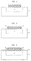
- FIG 1 shows the formation of a first polysilicon layer 14 over a portion of isolation region 12, which is formed in semiconductor substrate 10.
- Semiconductor substrate 10 is composed of a conventional semiconducting material including, but not limited to: Si, Ge, SiGe, GaAs, InAs, InP and all other III/V compound semiconductors. Layered substrates such as Si/Si or Si/SiGe are also contemplated herein. Of these semiconducting materials, it is preferred that the semiconductor substrate be composed of Si.
- the semiconductor substrate may be a p-type substrate or a n-type substrate depending on the type of MOS device to be present in the final BiCMOS structure.
- the isolation region may be a LOCOS (local oxidation of silicon) region or a trench isolation region, with preference given to a trench isolation region such as shown in FIG 1.
- LOCOS isolation local oxidation of silicon
- trench isolation region 12 is a trench isolation region, such as shown in FIG 1
- the isolation trench region is formed utilizing conventional lithography, etching and trench filling. Since the formation of isolation regions includes conventional processes well known to those skilled in the art, a detailed description concerning the same is not provided herein.
- First polysilicon layer 14 which will subsequently become the lower electrode of the poly-poly capacitor is also formed in the CMOS device region and will be used in the CMOS device region as the gate electrode of the CMOS device.
- First polysilicon layer 14 may be formed utilizing a conventional deposition process including, but not limited to: chemical vapor deposition (CVD), plasma-assisted CVD, sputtering, chemical solution deposition and other like deposition processes.
- the thickness of the first polysilicon layer may vary, but typically the first polysilicon layer has a thickness of from about 500 to about 5000 ⁇ , with a thickness of from about 1000 to about 2000 ⁇ being most preferred.
- first nitride spacers 16 are formed about the first polysilicon layer. Specifically, first nitride spacers 16 are formed on exposed vertical edges of the previously formed first polysilicon layer.
- the first nitride spacers which are composed of a conventional nitride material such as Si 3 N 4 are formed by a conventional deposition process such as CVD, plasma-assisted CVD and other like deposition processes, followed by lithography and etching.
- the etching process employed in forming first nitride spacers 16 is a conventional etching process which has a high selectivity for removing nitride as compared to polysilicon.
- FIG 3 shows the poly-poly capacitor structure after forming second nitride layer 18 over the structure shown in FIG 2.
- the second nitride layer is formed over first polysilicon layer 14 and first nitride spacers 16 utilizing a conventional deposition process which may be the same as or different from that used in forming the first nitride spacers.
- the second nitride layer may be composed of the same or a different nitride-containing material as the first nitride spacers. It is noted that the second nitride layer serves to protect the adjacent device regions during the formation of the poly-poly capacitor.
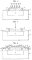
- ions of a first conductivity type (P- or N-type) 20 are implanted into the first polysilicon layer so as to form lower electrode 22 of the poly-poly capacitor, see FIG 4.
- the ion implantation used in forming the lower electrode of the poly-poly capacitor is carried out in a conventional ion implantation apparatus which is capable of operating at conventional implant energies.
- the concentration of the dopant ion used in this implant step may vary and is within values typically used by those skilled in the art.
- the type of dopant ion employed in this step is dependent upon the type of device to be fabricated.
- the second nitride layer is patterned utilizing conventional lithography and thereafter an etching process which has a high selectivity for removing nitride as compared to doped polysilicon is employed so as to form second nitride spacers 24, see FIG 5.
- second nitride layer 18 is etched so as to form a window 21 in the second nitride layer that exposes a portion of the underlying lower electrode.
- film stack 30 is formed on the structure shown in FIG 5.
- film stack 30 is composed of a layer of oxide 32, a second layer of polysilicon 34 and a layer of SiGe 36.
- the layer of oxide 32 is formed utilizing a conventional deposition process such as CVD or alternatively, oxide layer 32 can be formed by a conventional thermal growing process.
- the thickness of the oxide layer may vary, but typically, oxide layer 32 of film stack 30 has a thickness of from about 50 to about 200 ⁇ .
- Polysilicon layer 34 of film stack 30 is formed utilizing the same or a different deposition process as that used in forming first polysilicon layer 14.
- the thickness of polysilicon layer 34 may vary, but typically second polysilicon layer 34 of film stack 30 has a thickness of from about 100 to about 1000 ⁇ .
- SiGe layer 36 of film stack 30, which also is used in forming the SiGe base region of the bipolar transistor region (not shown), is formed utilizing a conventional deposition process including, but not limited to: ultra-high vacuum chemical vapor deposition (UHVCVD), molecular beam epitaxy (MBE), rapid thermal chemical vapor deposition (RTCVD), and plasma-enhanced chemical vapor deposition (PECVD).
- UHVCVD ultra-high vacuum chemical vapor deposition
- MBE molecular beam epitaxy
- RTCVD rapid thermal chemical vapor deposition
- PECVD plasma-enhanced chemical vapor deposition
- the SiGe thickness may vary, and thus is not limited to a specific thickness range.
- Each of the aforementioned deposition processes used in forming the SiGe layer include the use of conventional conditions that are well known to those skilled in the art. The conditions may vary depending on the type of deposition process used in forming the SiGe layer.
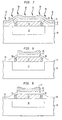
- SiGe layer 36 and second polysilicon layer 34 are subjected to an ion implantation process wherein ions of a second conductivity type 38 that are different from the first are implanted into layers 36 and 34.
- the above mentioned second ion implantation step is carried out in a conventional ion implantation apparatus which is capable of operating at conventional implant energies.
- the concentration of the dopant ion used in this implant step i.e., doping of layers 36 and 34, may vary and is dependent on the type of dopant implanted into the first polysilicon layer.
- This step to form doped layer 40 is shown in FIG 7. It is noted that doped layer 40 is a combination of SiGe layer 36 and second polysilicon 34. Moreover, doped layer 40 is to serve as the upper electrode of the poly-poly capacitor.
- doped layer 40 i.e., doped SiGe and doped second polysilicon layers
- doped layer 40 is subjected to conventional lithography and etching processes which are capable of patterning the doped SiGe+second polysilicon layer into upper electrode 40 forming the structure shown in FIG 8. It should be noted that during etching of the doped SiGe+second polysilicon layer, some of the underlying oxide layer may be also be etched.
- the upper electrode i.e., doped layer 40
- the upper electrode may be optionally subjected to another ion implantation process wherein additional second ions are implanted into the upper electrode. It is noted that this optional additional implant step forms source and drain regions (not shown in the drawings) in the CMOS device region.
- FIG 9 shows the structure after the exposed surfaces of the upper electrode have been subjected to a conventional salidication process wherein salicide region 42 is formed therein. The salidication process is carried utilizing conventional annealing temperatures and times well known to those skilled in the art.
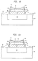
- FIGS 10-11 show additional processing steps that may be employed prior to conducting the salicidation process.
- FIG 10 shows the structure of FIG 9 which includes patterned protective nitride layer 44 formed on horizontal surfaces of the poly-poly capacitor.
- the patterned protective layer is formed by a conventional deposition process, followed by lithography and etching.
- FIG 11 shows the structure after conducting the above-mentioned salicidation process.
- FIGS 12-19 show a second embodiment of the present invention in which second nitride layer 18 remains in the structure throughout the various processing steps. This results in a high voltage poly-poly capacitor device.
- the processing steps used in forming the structures shown in FIGS 12-15 are identical to those shown in FIGS 1-4 above. Instead of etching the nitride layer as shown in FIG 5, the nitride layer in this embodiment is not etched and film stack 30 is formed thereon utilizing the processing steps mentioned above so as to provide the structure shown in FIG 16.
- FIGS 17-19 are identical to FIGS 7-9 with the exception that the poly-poly capacitor includes second nitride layer 18 therein.
Abstract
Description
- The present invention relates generally to BiCMOS (i.e., bipolar and complementary metal oxide semiconductor (CMOS)) technology, and more particularly to the fabrication of a polysilicon to polysilicon (poly-poly) capacitor.
- In the field of semiconductor device manufacturing, CMOS and BiCMOS technologies have been widely used for integrating highly complex analog-digital subsystems onto a single chip. In such subsystems, high precision capacitors are typically required.
- Several types of capacitors are presently available including diffusion-poly capacitors, poly-poly capacitors and metal-metal capacitors. In order to meet the demand for high precision capacitors in today's generation of integrated devices, poly-poly capacitors have been increasingly used.
- Despite its high precision, a poly-poly capacitor is a compromise between high cost and ideal capacitor characteristics since it is relatively easy to construct, and has electrical characteristics that are better than diffusion-poly capacitors, but inferior to metal-metal capacitors. However, a metal-metal capacitor is much more difficult to fabricate than a poly-poly capacitor. Moreover, poly-poly capacitors are known to have a more linear V-C relationship than MOS (i.e., diffusion-poly) capacitors.
- In addition, the dielectric for MOS capacitors results from an oxide that is thermally grown over a highly doped diffusion region. In contrast, the dielectric for a poly-poly capacitor is generally a deposited chemical vapor deposition (CVD) oxide and reliability requirements cause the resulting oxide to be thicker than can be realized with a thermal oxide. Therefore, higher capacitance values generally result for MOS capacitors than poly-poly capacitors.
- Although various methods of forming poly-poly capacitors are known, most prior art methods are not suitable for integration with BiCMOS processing schemes. United States Patent No. 6025219 discloses a BiCMOS processing scheme where a polysilicon base electrode is formed together with an upper capacitor electrode, and CMOS gate electrodes are formed together with a lower capacitor electrode. However, no SiGe process is disclosed in patent US-625219. In view of the BiCMOS integration problem with prior art methods, there is a continued need for developing a new and improved method of fabricating a poly-poly capacitor utilizing existing polysilicon layers and masking steps employed in conventional BiCMOS processes.
- Accordingly, the invention provides a method of fabricating a poly-poly capacitor in which the bottom plate of the capacitor is formed from a gate of a MOS transistor, and the top plate of the capacitor is formed from the base region of a heterojunction bipolar transistor.
- Preferably a lower polysilicon layer of the capacitor is formed during deposition of a CMOS gate electrode and an upper SiGe polysilicon layer of the capacitor is formed during the growth of a base region of an SiGe heterojunction bipolar transistor. The doped first layer of polysilicon serves as the lower electrode of the poly-poly capacitor, whereas the doped SiGe layer together with the doped second layer of polysilicon serve as an upper electrode of the poly-poly capacitor.
- This approach for fabricating a poly-poly capacitor for use in CMOS or BiCMOS integrated circuits is neither complicated nor expensive, and utilises existing polysilicon and masking steps, thereby permitting the integration of the poly-poly capacitor into a BiCMOS device at a low cost. Steps and structures that are typically used to form the gate of the MOS transistor and SiGe base structure of the bipolar transistor in a BiCMOS process can be utilised.
- A first preferred embodiment of the present invention provides a method comprising the steps of:
- (a) forming a first polysilicon layer over a portion of an isolation region in a device region in which a poly-poly capacitor is to be formed;
- (b) forming first nitride spacers about said first polysilicon layer;
- (c) depositing a nitride layer over said first polysilicon layer and said first nitride spacers;
- (d) implanting ions of a first conductivity type into said first polysilicon layer so as to form a lower electrode of said poly-poly capacitor;
- (e) removing portions of said nitride layer so as to form second nitride spacers and to expose a portion of said lower electrode;
- (f) forming a film stack on at least said exposed portion of said lower electrode, said film stack comprising an oxide layer, a second layer of polysilicon and a layer of SiGe;
- (g) implanting ions of a second conductivity type that are different from said first conductivity type into said layer of SiGe and said second layer of polysilicon;
- (h) etching at least said layer of SiGe and said second layer of polysilicon so as to form an upper electrode of said poly-poly capacitor; and
- (i) saliciding all exposed surfaces of said upper electrode.
- The above processing steps are typically used for forming a high capacitance poly-poly capacitor.
- A second embodiment of the present invention, in which a high voltage device can be formed, provides a method comprising the steps of:
- (a) forming a first polysilicon layer over a portion of an isolation region in a device region in which a poly-poly capacitor is to be formed;
- (b) forming first nitride spacers about said first polysilicon layer;
- (c) depositing a nitride layer over said first polysilicon layer and said first nitride spacers;
- (d) implanting ions of a first conductivity type into said first polysilicon layer so as to form a lower electrode of said poly-poly capacitor;
- (e) forming a film stack on at least said nitride layer, said film stack comprising an oxide layer, a second layer of polysilicon and a layer of SiGe;
- (f) implanting ions of a second conductivity type that are different from said first conductivity type into said layer of SiGe and said second layer of polysilicon;
- (g) etching at least said layer of SiGe and said second layer of polysilicon so as to form an upper electrode of said poly-poly capacitor; and
- (h) saliciding all exposed surfaces of said upper electrode.
- In both the first and second embodiment a patterned protective nitride layer can be formed on at least a portion of the exposed upper electrode prior to salicidation.
- Various preferred embodiments of the invention will now be described in detail by way of example only, with reference to the following drawings:
- FIGS 1-9 are cross-sectional views of a poly-poly capacitor through various processing steps used in a first implementation of the present invention.
- FIGS 10-11 show an optional processing step wherein a patterned protective nitride layer is employed in the first implementation of the present invention.
- FIGS 12-19 are cross-sectional views of a poly-poly capacitor through various processing steps used in a second implementation of the present invention.
- FIGS 20-21 show an optional processing step wherein a patterned protective nitride layer is employed in the second implementation of the present invention.
- Reference is first made to FIGS 1-9 which illustrate the formation of a high capacitance poly-poly capacitor through various processing steps in accordance with a first embodiment of the present invention. Specifically, FIG 1 shows the formation of a
first polysilicon layer 14 over a portion ofisolation region 12, which is formed insemiconductor substrate 10.Semiconductor substrate 10 is composed of a conventional semiconducting material including, but not limited to: Si, Ge, SiGe, GaAs, InAs, InP and all other III/V compound semiconductors. Layered substrates such as Si/Si or Si/SiGe are also contemplated herein. Of these semiconducting materials, it is preferred that the semiconductor substrate be composed of Si. The semiconductor substrate may be a p-type substrate or a n-type substrate depending on the type of MOS device to be present in the final BiCMOS structure. - The isolation region may be a LOCOS (local oxidation of silicon) region or a trench isolation region, with preference given to a trench isolation region such as shown in FIG 1. When LOCOS isolation is employed, conventional oxidation processes well known to those skilled in the art are used in forming
region 12. On the other hand, whenisolation region 12 is a trench isolation region, such as shown in FIG 1, the isolation trench region is formed utilizing conventional lithography, etching and trench filling. Since the formation of isolation regions includes conventional processes well known to those skilled in the art, a detailed description concerning the same is not provided herein. -
First polysilicon layer 14 which will subsequently become the lower electrode of the poly-poly capacitor is also formed in the CMOS device region and will be used in the CMOS device region as the gate electrode of the CMOS device.First polysilicon layer 14 may be formed utilizing a conventional deposition process including, but not limited to: chemical vapor deposition (CVD), plasma-assisted CVD, sputtering, chemical solution deposition and other like deposition processes. The thickness of the first polysilicon layer may vary, but typically the first polysilicon layer has a thickness of from about 500 to about 5000 Å, with a thickness of from about 1000 to about 2000 Å being most preferred. - Next, and as illustrated in FIG 2,
first nitride spacers 16 are formed about the first polysilicon layer. Specifically,first nitride spacers 16 are formed on exposed vertical edges of the previously formed first polysilicon layer. The first nitride spacers which are composed of a conventional nitride material such as Si3N4 are formed by a conventional deposition process such as CVD, plasma-assisted CVD and other like deposition processes, followed by lithography and etching. The etching process employed in formingfirst nitride spacers 16 is a conventional etching process which has a high selectivity for removing nitride as compared to polysilicon. - FIG 3 shows the poly-poly capacitor structure after forming
second nitride layer 18 over the structure shown in FIG 2. Specifically, the second nitride layer is formed overfirst polysilicon layer 14 andfirst nitride spacers 16 utilizing a conventional deposition process which may be the same as or different from that used in forming the first nitride spacers. Moreover, the second nitride layer may be composed of the same or a different nitride-containing material as the first nitride spacers. It is noted that the second nitride layer serves to protect the adjacent device regions during the formation of the poly-poly capacitor. - With the second nitride layer in place, ions of a first conductivity type (P- or N-type) 20 are implanted into the first polysilicon layer so as to form
lower electrode 22 of the poly-poly capacitor, see FIG 4. The ion implantation used in forming the lower electrode of the poly-poly capacitor is carried out in a conventional ion implantation apparatus which is capable of operating at conventional implant energies. The concentration of the dopant ion used in this implant step may vary and is within values typically used by those skilled in the art. Moreover, the type of dopant ion employed in this step is dependent upon the type of device to be fabricated. - In accordance with the first embodiment of the present invention for making high capacitance poly-poly capacitors, the second nitride layer is patterned utilizing conventional lithography and thereafter an etching process which has a high selectivity for removing nitride as compared to doped polysilicon is employed so as to form
second nitride spacers 24, see FIG 5. Specifically,second nitride layer 18 is etched so as to form awindow 21 in the second nitride layer that exposes a portion of the underlying lower electrode. - Next, and as is illustrated in FIG 6,
film stack 30 is formed on the structure shown in FIG 5. In accordance with the present invention,film stack 30 is composed of a layer ofoxide 32, a second layer ofpolysilicon 34 and a layer ofSiGe 36. The layer ofoxide 32 is formed utilizing a conventional deposition process such as CVD or alternatively,oxide layer 32 can be formed by a conventional thermal growing process. The thickness of the oxide layer may vary, but typically,oxide layer 32 offilm stack 30 has a thickness of from about 50 to about 200 Å. -
Polysilicon layer 34 offilm stack 30 is formed utilizing the same or a different deposition process as that used in formingfirst polysilicon layer 14. The thickness ofpolysilicon layer 34 may vary, but typicallysecond polysilicon layer 34 offilm stack 30 has a thickness of from about 100 to about 1000 Å. -
SiGe layer 36 offilm stack 30, which also is used in forming the SiGe base region of the bipolar transistor region (not shown), is formed utilizing a conventional deposition process including, but not limited to: ultra-high vacuum chemical vapor deposition (UHVCVD), molecular beam epitaxy (MBE), rapid thermal chemical vapor deposition (RTCVD), and plasma-enhanced chemical vapor deposition (PECVD). It is noted that the SiGe thickness may vary, and thus is not limited to a specific thickness range. Each of the aforementioned deposition processes used in forming the SiGe layer include the use of conventional conditions that are well known to those skilled in the art. The conditions may vary depending on the type of deposition process used in forming the SiGe layer. - After
film stack 30 has been formed over the exposed lower electrode,SiGe layer 36 andsecond polysilicon layer 34 are subjected to an ion implantation process wherein ions of asecond conductivity type 38 that are different from the first are implanted intolayers
Specifically, the above mentioned second ion implantation step is carried out in a conventional ion implantation apparatus which is capable of operating at conventional implant energies. The concentration of the dopant ion used in this implant step, i.e., doping oflayers layer 40 is shown in FIG 7. It is noted that dopedlayer 40 is a combination ofSiGe layer 36 andsecond polysilicon 34. Moreover, dopedlayer 40 is to serve as the upper electrode of the poly-poly capacitor. - After doping the SiGe and second polysilicon layers with ions of a second conductivity type, doped layer 40 (i.e., doped SiGe and doped second polysilicon layers) is subjected to conventional lithography and etching processes which are capable of patterning the doped SiGe+second polysilicon layer into
upper electrode 40 forming the structure shown in FIG 8. It should be noted that during etching of the doped SiGe+second polysilicon layer, some of the underlying oxide layer may be also be etched. - Following this step, the upper electrode, i.e., doped
layer 40, may be optionally subjected to another ion implantation process wherein additional second ions are implanted into the upper electrode. It is noted that this optional additional implant step forms source and drain regions (not shown in the drawings) in the CMOS device region. FIG 9 shows the structure after the exposed surfaces of the upper electrode have been subjected to a conventional salidication process whereinsalicide region 42 is formed therein. The salidication process is carried utilizing conventional annealing temperatures and times well known to those skilled in the art. - FIGS 10-11 show additional processing steps that may be employed prior to conducting the salicidation process. Specifically, FIG 10 shows the structure of FIG 9 which includes patterned
protective nitride layer 44 formed on horizontal surfaces of the poly-poly capacitor. The patterned protective layer is formed by a conventional deposition process, followed by lithography and etching. FIG 11 shows the structure after conducting the above-mentioned salicidation process. - FIGS 12-19 show a second embodiment of the present invention in which
second nitride layer 18 remains in the structure throughout the various processing steps. This results in a high voltage poly-poly capacitor device. Specifically, the processing steps used in forming the structures shown in FIGS 12-15 are identical to those shown in FIGS 1-4 above. Instead of etching the nitride layer as shown in FIG 5, the nitride layer in this embodiment is not etched andfilm stack 30 is formed thereon utilizing the processing steps mentioned above so as to provide the structure shown in FIG 16. FIGS 17-19 are identical to FIGS 7-9 with the exception that the poly-poly capacitor includessecond nitride layer 18 therein. - FIGS. 20-21 show an optional step of the second embodiment wherein a patterned protective nitride layer is employed.
Claims (12)
- A method for fabricating a poly-dielectric-poly-SiGe capacitor integrated with a BiCMOS process comprising:forming a first polysilicon layer (14) subsequently forming a lower plate electrode (22) of the poly-dielectric-poly-SiGe capacitor during deposition of a gate electrode of a CMOS transistor; andforming an film stack, the film stack comprising a layer of oxide (32), a second layer of polysilicon (34) and a layer of SiGe (36) whereby the layer of SiGe (36) is subsequently forming an upper plate electrode (40) of poly-dielectric-poly-SiGe capacitor and is used to form the SiGe base region of a heterojunction bipolar transistor.
- The method of Claim 1 wherein said lower plate electrode is formed by the steps of:forming a first polysilicon layer (14) over a portion of an isolation region (12) in a device region in which apoly-dielectric-poly-SiGe capacitor is to be formed;forming first nitride spacers (16) about said first polysilicon layer (14);depositing a nitride layer (18) over said first polysilicon layer (14) and said first nitride spacers (16); andimplanting ions of a first conductivity type into said first polysilicon layer (14) so as to form said lower plate electrode (22) of said poly-poly capacitor.
- The method of Claim 2 wherein said upper SiGe plate electrode (40) is formed by the steps of:removing portions of said nitride layer (18) so as to form second nitride spacers (24) and to expose a portion of said lower plate electrode (22);forming a film stack on at least said exposed portion of said lower plate electrode (22) said film stack comprising an oxidelayer (32), a second layer of polysilicon (34) and a layer of SiGe (36);implanting ions of a second conductivity type that are different from said first conductivity type into said layer of SiGe (36) and said second layer of polysilicon (34);etching at least said layer of SiGe (36) and said second layer of polysilicon (34) so as to form said upper plate electrode (40) of said poly-dielectric-poly-SiGe capacitor; andsaliciding all exposed surfaces of said upper SiGe plate electrode (40).
- The method of Claim 2 wherein said upper SiGe plate electrode (40) is formed by the steps of:forming a film stack on at least said nitride layer (18) said film stack comprising an oxide layer (32), a second layer of polysilicon (34) and a layer of SiGe (36);implanting ions of a second conductivity type that are different from said first conductivity type into said layer of SiGe (36) and said second layer of polysilicon (34);etching at least said layer of SiGe (36) and said second layer of polysilicon (34) so as to form said upper SiGe plate electrode (40) of said poly-dielectric-poly-SiGe capacitor; andsaliciding all exposed surfaces of said upper SiGe plate electrode (40).
- The method of Claim 3 or 4 wherein a patterned protective nitride layer (44) is formed on portions of said upper SiGe plate electrode (40) prior to salicidation.
- The method of any of Claims 2 to 5, wherein said first polysilicon layer (14) is formed by a deposition process selected from the group consisting of chemical vapor deposition (CVD), plasma-assisted CVD, sputtering and chemical solution deposition.
- The method of any of Claims 2 to 6, wherein said first nitride spacers (16) are formed by deposition and etching.
- The method of any of Claims 2 to 6, wherein said nitride layer (18) is formed by a deposition process selected from CVD, plasma-assisted CVD, sputtering and chemical solution deposition.
- The method of any preceding Claim, wherein said SiGe base region is formed from a deposition process selected from the group consisting of ultra-high vacuum chemical vapor deposition (UHVCVD), molecular beam epitaxy (MBE), rapid thermal chemical vapor deposition (RTCVD) and plasma-enhanced chemical vapor deposition (PECVD).
- A device fabricated according to the method of any preceding claim.
- A poly-dielectric-poly-SiGe capacitor integrated with a BiCMOS comprising:a first polysilicon layer (14) subsequently forming a lower plate electrode (22) of the poly-dielectric-poly-SiGe capacitor and a gate electrode of a CMOS transistor; anda film stack, the film stack comprising a layer of oxide (32), a second layer of polysilicon (34) and a layer of SiGe (36) whereby the layer of SiGe (36) is subsequently forming an upper plate electrode (40) of the poly-dielectric-poly-SiGe capacitor and is used to form the SiGe base region of a heterojunction bipolar transistor.
- A semi-conductor device including the poly-dielectric-poly-SiGe capacitor of claim 11.
Applications Claiming Priority (2)
| Application Number | Priority Date | Filing Date | Title |
|---|---|---|---|
| US09/745,361 US6440811B1 (en) | 2000-12-21 | 2000-12-21 | Method of fabricating a poly-poly capacitor with a SiGe BiCMOS integration scheme |
| US745361 | 2000-12-21 |
Publications (3)
| Publication Number | Publication Date |
|---|---|
| EP1225628A2 EP1225628A2 (en) | 2002-07-24 |
| EP1225628A3 EP1225628A3 (en) | 2004-11-10 |
| EP1225628B1 true EP1225628B1 (en) | 2006-06-21 |
Family
ID=24996373
Family Applications (1)
| Application Number | Title | Priority Date | Filing Date |
|---|---|---|---|
| EP01308085A Expired - Lifetime EP1225628B1 (en) | 2000-12-21 | 2001-09-24 | CMOS capacitor fabrication |
Country Status (8)
| Country | Link |
|---|---|
| US (1) | US6440811B1 (en) |
| EP (1) | EP1225628B1 (en) |
| JP (1) | JP3782962B2 (en) |
| KR (1) | KR100407538B1 (en) |
| AT (1) | ATE331299T1 (en) |
| DE (1) | DE60120897T2 (en) |
| SG (1) | SG96266A1 (en) |
| TW (1) | TW543155B (en) |
Families Citing this family (9)
| Publication number | Priority date | Publication date | Assignee | Title |
|---|---|---|---|---|
| US6426265B1 (en) * | 2001-01-30 | 2002-07-30 | International Business Machines Corporation | Incorporation of carbon in silicon/silicon germanium epitaxial layer to enhance yield for Si-Ge bipolar technology |
| US6911964B2 (en) * | 2002-11-07 | 2005-06-28 | Duke University | Frame buffer pixel circuit for liquid crystal display |
| JP4789421B2 (en) * | 2003-03-12 | 2011-10-12 | 三星電子株式会社 | Semiconductor device having photon absorption film and method for manufacturing the same |
| TWI233689B (en) * | 2003-04-14 | 2005-06-01 | Samsung Electronics Co Ltd | Capacitors of semiconductor devices including silicon-germanium and metallic electrodes and methods of fabricating the same |
| KR100618869B1 (en) * | 2004-10-22 | 2006-09-13 | 삼성전자주식회사 | Semiconductor device including capacitor and method for fabricating the same |
| KR100617057B1 (en) * | 2004-12-30 | 2006-08-30 | 동부일렉트로닉스 주식회사 | Structure for Capacitor and Fabricating Method Thereof |
| KR100634241B1 (en) * | 2005-05-30 | 2006-10-13 | 삼성전자주식회사 | Semiconductor capacitor and method of manufacturing the same |
| KR100731087B1 (en) * | 2005-10-28 | 2007-06-22 | 동부일렉트로닉스 주식회사 | BiCMOS device for using power and method for manufacturing the same |
| US11355617B2 (en) * | 2019-10-01 | 2022-06-07 | Qualcomm Incorporated | Self-aligned collector heterojunction bipolar transistor (HBT) |
Family Cites Families (19)
| Publication number | Priority date | Publication date | Assignee | Title |
|---|---|---|---|---|
| JPS5823470A (en) * | 1981-08-06 | 1983-02-12 | Oki Electric Ind Co Ltd | Semiconductor device |
| US4914546A (en) * | 1989-02-03 | 1990-04-03 | Micrel Incorporated | Stacked multi-polysilicon layer capacitor |
| US5195017A (en) | 1989-12-13 | 1993-03-16 | Texas Instruments Incorporated | Method for forming a polysilicon to polysilicon capacitor and apparatus formed therefrom |
| US5104822A (en) * | 1990-07-30 | 1992-04-14 | Ramtron Corporation | Method for creating self-aligned, non-patterned contact areas and stacked capacitors using the method |
| WO1992014262A1 (en) | 1991-02-01 | 1992-08-20 | Sierra Semiconductor Corporation | Semiconductor structure and method for making same |
| US5130885A (en) * | 1991-07-10 | 1992-07-14 | Micron Technology, Inc. | Dram cell in which a silicon-germanium alloy layer having a rough surface morphology is utilized for a capacitive surface |
| JP2630874B2 (en) * | 1991-07-29 | 1997-07-16 | 三洋電機株式会社 | Method for manufacturing semiconductor integrated circuit |
| US5173437A (en) | 1991-08-01 | 1992-12-22 | Chartered Semiconductor Manufacturing Pte Ltd | Double polysilicon capacitor formation compatable with submicron processing |
| US5286991A (en) | 1992-08-26 | 1994-02-15 | Pioneer Semiconductor Corporation | Capacitor for a BiCMOS device |
| JP2616569B2 (en) | 1994-09-29 | 1997-06-04 | 日本電気株式会社 | Method for manufacturing semiconductor integrated circuit device |
| JP2621821B2 (en) | 1995-03-06 | 1997-06-18 | 日本電気株式会社 | Method for manufacturing capacitive element of semiconductor storage device |
| FR2756103B1 (en) * | 1996-11-19 | 1999-05-14 | Sgs Thomson Microelectronics | MANUFACTURE OF BIPOLAR / CMOS INTEGRATED CIRCUITS AND A CAPACITOR |
| JP2953425B2 (en) * | 1997-03-31 | 1999-09-27 | 日本電気株式会社 | Method for manufacturing semiconductor device |
| US5939753A (en) | 1997-04-02 | 1999-08-17 | Motorola, Inc. | Monolithic RF mixed signal IC with power amplification |
| CN1112731C (en) | 1997-04-30 | 2003-06-25 | 三星电子株式会社 | Method for making capacitor used for analog function |
| US5930635A (en) * | 1997-05-02 | 1999-07-27 | National Semiconductor Corporation | Complementary Si/SiGe heterojunction bipolar technology |
| US6150706A (en) * | 1998-02-27 | 2000-11-21 | Micron Technology, Inc. | Capacitor/antifuse structure having a barrier-layer electrode and improved barrier layer |
| US6218315B1 (en) * | 2000-02-24 | 2001-04-17 | International Business Machines Corporation | HTO (high temperature oxide) deposition for capacitor dielectrics |
| US6507063B2 (en) * | 2000-04-17 | 2003-01-14 | International Business Machines Corporation | Poly-poly/MOS capacitor having a gate encapsulating first electrode layer |
-
2000
- 2000-12-21 US US09/745,361 patent/US6440811B1/en not_active Expired - Lifetime
-
2001
- 2001-09-24 AT AT01308085T patent/ATE331299T1/en not_active IP Right Cessation
- 2001-09-24 DE DE60120897T patent/DE60120897T2/en not_active Expired - Lifetime
- 2001-09-24 EP EP01308085A patent/EP1225628B1/en not_active Expired - Lifetime
- 2001-12-04 JP JP2001369481A patent/JP3782962B2/en not_active Expired - Fee Related
- 2001-12-11 KR KR10-2001-0078343A patent/KR100407538B1/en not_active IP Right Cessation
- 2001-12-13 SG SG200107801A patent/SG96266A1/en unknown
- 2001-12-14 TW TW090131170A patent/TW543155B/en not_active IP Right Cessation
Also Published As
| Publication number | Publication date |
|---|---|
| US6440811B1 (en) | 2002-08-27 |
| KR20020050702A (en) | 2002-06-27 |
| DE60120897T2 (en) | 2006-12-21 |
| KR100407538B1 (en) | 2003-11-28 |
| DE60120897D1 (en) | 2006-08-03 |
| SG96266A1 (en) | 2003-05-23 |
| ATE331299T1 (en) | 2006-07-15 |
| JP3782962B2 (en) | 2006-06-07 |
| EP1225628A3 (en) | 2004-11-10 |
| TW543155B (en) | 2003-07-21 |
| JP2002237541A (en) | 2002-08-23 |
| EP1225628A2 (en) | 2002-07-24 |
Similar Documents
| Publication | Publication Date | Title |
|---|---|---|
| US5405790A (en) | Method of forming a semiconductor structure having MOS, bipolar, and varactor devices | |
| EP1148557B1 (en) | Stacked capacitor and method of fabricating the stacked capacitor | |
| US8395217B1 (en) | Isolation in CMOSFET devices utilizing buried air bags | |
| US7737500B2 (en) | CMOS diodes with dual gate conductors, and methods for forming the same | |
| US6420747B2 (en) | MOSCAP design for improved reliability | |
| US5675176A (en) | Semiconductor device and a method for manufacturing the same | |
| US7785974B2 (en) | Methods of employing a thin oxide mask for high dose implants | |
| US6670228B2 (en) | Method of fabricating a polysilicon capacitor utilizing FET and bipolar base polysilicon layers | |
| KR20010110769A (en) | SEMICONDUCTOR DEVICE WITH AN INTEGRATED CMOS CIRCUIT WITH MOS TRANSISTORS HAVING SILICON-GERMANIUM (Si1-xGex) GATE ELECTRODES, AND METHOD OF MANUFACTURING SAME | |
| US6461925B1 (en) | Method of manufacturing a heterojunction BiCMOS integrated circuit | |
| EP1225628B1 (en) | CMOS capacitor fabrication | |
| US7847401B2 (en) | Methods, systems and structures for forming semiconductor structures incorporating high-temperature processing steps | |
| US6856000B2 (en) | Reduce 1/f noise in NPN transistors without degrading the properties of PNP transistors in integrated circuit technologies | |
| US8263453B2 (en) | Method for forming semiconductor devices with active silicon height variation | |
| EP0614218A1 (en) | Method for manufacturing capacitor and MIS transistor | |
| JPH1093077A (en) | Semiconductor device and manufacturing method thereof | |
| US11843034B2 (en) | Lateral bipolar transistor | |
| WO1997049131A1 (en) | Semiconductor device with buried conductive silicide layer | |
| KR19980034371A (en) | Dual Gate CMOS Device Manufacturing Method |
Legal Events
| Date | Code | Title | Description |
|---|---|---|---|
| PUAI | Public reference made under article 153(3) epc to a published international application that has entered the european phase |
Free format text: ORIGINAL CODE: 0009012 |
|
| AK | Designated contracting states |
Kind code of ref document: A2 Designated state(s): AT BE CH CY DE DK ES FI FR GB GR IE IT LI LU MC NL PT SE TR |
|
| AX | Request for extension of the european patent |
Free format text: AL;LT;LV;MK;RO;SI |
|
| PUAL | Search report despatched |
Free format text: ORIGINAL CODE: 0009013 |
|
| AK | Designated contracting states |
Kind code of ref document: A3 Designated state(s): AT BE CH CY DE DK ES FI FR GB GR IE IT LI LU MC NL PT SE TR |
|
| AX | Request for extension of the european patent |
Extension state: AL LT LV MK RO SI |
|
| 17P | Request for examination filed |
Effective date: 20041126 |
|
| 17Q | First examination report despatched |
Effective date: 20050309 |
|
| AKX | Designation fees paid |
Designated state(s): AT BE CH CY DE DK ES FI FR GB GR IE IT LI LU MC NL PT SE TR |
|
| GRAC | Information related to communication of intention to grant a patent modified |
Free format text: ORIGINAL CODE: EPIDOSCIGR1 |
|
| GRAP | Despatch of communication of intention to grant a patent |
Free format text: ORIGINAL CODE: EPIDOSNIGR1 |
|
| GRAS | Grant fee paid |
Free format text: ORIGINAL CODE: EPIDOSNIGR3 |
|
| GRAA | (expected) grant |
Free format text: ORIGINAL CODE: 0009210 |
|
| AK | Designated contracting states |
Kind code of ref document: B1 Designated state(s): AT BE CH CY DE DK ES FI FR GB GR IE IT LI LU MC NL PT SE TR |
|
| PG25 | Lapsed in a contracting state [announced via postgrant information from national office to epo] |
Ref country code: NL Free format text: LAPSE BECAUSE OF FAILURE TO SUBMIT A TRANSLATION OF THE DESCRIPTION OR TO PAY THE FEE WITHIN THE PRESCRIBED TIME-LIMIT Effective date: 20060621 Ref country code: CH Free format text: LAPSE BECAUSE OF FAILURE TO SUBMIT A TRANSLATION OF THE DESCRIPTION OR TO PAY THE FEE WITHIN THE PRESCRIBED TIME-LIMIT Effective date: 20060621 Ref country code: IT Free format text: LAPSE BECAUSE OF FAILURE TO SUBMIT A TRANSLATION OF THE DESCRIPTION OR TO PAY THE FEE WITHIN THE PRESCRIBED TIME-LIMIT;WARNING: LAPSES OF ITALIAN PATENTS WITH EFFECTIVE DATE BEFORE 2007 MAY HAVE OCCURRED AT ANY TIME BEFORE 2007. THE CORRECT EFFECTIVE DATE MAY BE DIFFERENT FROM THE ONE RECORDED. Effective date: 20060621 Ref country code: FI Free format text: LAPSE BECAUSE OF FAILURE TO SUBMIT A TRANSLATION OF THE DESCRIPTION OR TO PAY THE FEE WITHIN THE PRESCRIBED TIME-LIMIT Effective date: 20060621 Ref country code: BE Free format text: LAPSE BECAUSE OF FAILURE TO SUBMIT A TRANSLATION OF THE DESCRIPTION OR TO PAY THE FEE WITHIN THE PRESCRIBED TIME-LIMIT Effective date: 20060621 Ref country code: LI Free format text: LAPSE BECAUSE OF FAILURE TO SUBMIT A TRANSLATION OF THE DESCRIPTION OR TO PAY THE FEE WITHIN THE PRESCRIBED TIME-LIMIT Effective date: 20060621 Ref country code: AT Free format text: LAPSE BECAUSE OF FAILURE TO SUBMIT A TRANSLATION OF THE DESCRIPTION OR TO PAY THE FEE WITHIN THE PRESCRIBED TIME-LIMIT Effective date: 20060621 |
|
| REG | Reference to a national code |
Ref country code: GB Ref legal event code: FG4D |
|
| REG | Reference to a national code |
Ref country code: CH Ref legal event code: EP Ref country code: CH Ref legal event code: NV Representative=s name: INTERNATIONAL BUSINESS MACHINES CORPORATION |
|
| REG | Reference to a national code |
Ref country code: IE Ref legal event code: FG4D |
|
| REF | Corresponds to: |
Ref document number: 60120897 Country of ref document: DE Date of ref document: 20060803 Kind code of ref document: P |
|
| PG25 | Lapsed in a contracting state [announced via postgrant information from national office to epo] |
Ref country code: SE Free format text: LAPSE BECAUSE OF FAILURE TO SUBMIT A TRANSLATION OF THE DESCRIPTION OR TO PAY THE FEE WITHIN THE PRESCRIBED TIME-LIMIT Effective date: 20060921 Ref country code: DK Free format text: LAPSE BECAUSE OF FAILURE TO SUBMIT A TRANSLATION OF THE DESCRIPTION OR TO PAY THE FEE WITHIN THE PRESCRIBED TIME-LIMIT Effective date: 20060921 |
|
| PG25 | Lapsed in a contracting state [announced via postgrant information from national office to epo] |
Ref country code: IE Free format text: LAPSE BECAUSE OF NON-PAYMENT OF DUE FEES Effective date: 20060925 |
|
| PG25 | Lapsed in a contracting state [announced via postgrant information from national office to epo] |
Ref country code: MC Free format text: LAPSE BECAUSE OF NON-PAYMENT OF DUE FEES Effective date: 20060930 |
|
| PG25 | Lapsed in a contracting state [announced via postgrant information from national office to epo] |
Ref country code: ES Free format text: LAPSE BECAUSE OF FAILURE TO SUBMIT A TRANSLATION OF THE DESCRIPTION OR TO PAY THE FEE WITHIN THE PRESCRIBED TIME-LIMIT Effective date: 20061002 |
|
| PG25 | Lapsed in a contracting state [announced via postgrant information from national office to epo] |
Ref country code: PT Free format text: LAPSE BECAUSE OF FAILURE TO SUBMIT A TRANSLATION OF THE DESCRIPTION OR TO PAY THE FEE WITHIN THE PRESCRIBED TIME-LIMIT Effective date: 20061121 |
|
| NLV1 | Nl: lapsed or annulled due to failure to fulfill the requirements of art. 29p and 29m of the patents act | ||
| REG | Reference to a national code |
Ref country code: CH Ref legal event code: PL |
|
| ET | Fr: translation filed | ||
| PLBE | No opposition filed within time limit |
Free format text: ORIGINAL CODE: 0009261 |
|
| STAA | Information on the status of an ep patent application or granted ep patent |
Free format text: STATUS: NO OPPOSITION FILED WITHIN TIME LIMIT |
|
| 26N | No opposition filed |
Effective date: 20070322 |
|
| PG25 | Lapsed in a contracting state [announced via postgrant information from national office to epo] |
Ref country code: GR Free format text: LAPSE BECAUSE OF FAILURE TO SUBMIT A TRANSLATION OF THE DESCRIPTION OR TO PAY THE FEE WITHIN THE PRESCRIBED TIME-LIMIT Effective date: 20060922 |
|
| PG25 | Lapsed in a contracting state [announced via postgrant information from national office to epo] |
Ref country code: TR Free format text: LAPSE BECAUSE OF FAILURE TO SUBMIT A TRANSLATION OF THE DESCRIPTION OR TO PAY THE FEE WITHIN THE PRESCRIBED TIME-LIMIT Effective date: 20060621 Ref country code: LU Free format text: LAPSE BECAUSE OF NON-PAYMENT OF DUE FEES Effective date: 20060924 |
|
| REG | Reference to a national code |
Ref country code: GB Ref legal event code: 746 Effective date: 20080808 |
|
| PG25 | Lapsed in a contracting state [announced via postgrant information from national office to epo] |
Ref country code: CY Free format text: LAPSE BECAUSE OF FAILURE TO SUBMIT A TRANSLATION OF THE DESCRIPTION OR TO PAY THE FEE WITHIN THE PRESCRIBED TIME-LIMIT Effective date: 20060621 |
|
| PGFP | Annual fee paid to national office [announced via postgrant information from national office to epo] |
Ref country code: FR Payment date: 20110928 Year of fee payment: 11 |
|
| REG | Reference to a national code |
Ref country code: FR Ref legal event code: ST Effective date: 20130531 |
|
| PG25 | Lapsed in a contracting state [announced via postgrant information from national office to epo] |
Ref country code: FR Free format text: LAPSE BECAUSE OF NON-PAYMENT OF DUE FEES Effective date: 20121001 |
|
| PGFP | Annual fee paid to national office [announced via postgrant information from national office to epo] |
Ref country code: GB Payment date: 20150923 Year of fee payment: 15 |
|
| REG | Reference to a national code |
Ref country code: DE Ref legal event code: R081 Ref document number: 60120897 Country of ref document: DE Owner name: GLOBALFOUNDRIES INC., KY Free format text: FORMER OWNER: INTERNATIONAL BUSINESS MACHINES CORPORATION, ARMONK, NY, US Ref country code: DE Ref legal event code: R082 Ref document number: 60120897 Country of ref document: DE Representative=s name: RICHARDT PATENTANWAELTE PARTG MBB, DE Ref country code: DE Ref legal event code: R081 Ref document number: 60120897 Country of ref document: DE Owner name: GLOBALFOUNDRIES INC., KY Free format text: FORMER OWNER: INTERNATIONAL BUSINESS MACHINES CORPORATION, ARMONK, N.Y., US |
|
| REG | Reference to a national code |
Ref country code: DE Ref legal event code: R081 Ref document number: 60120897 Country of ref document: DE Owner name: GLOBALFOUNDRIES INC., KY Free format text: FORMER OWNER: GLOBALFOUNDRIES US 2 LLC (N.D.GES.DES STAATES DELAWARE), HOPEWELL JUNCTION, N.Y., US Ref country code: DE Ref legal event code: R082 Ref document number: 60120897 Country of ref document: DE Representative=s name: RICHARDT PATENTANWAELTE PARTG MBB, DE |
|
| REG | Reference to a national code |
Ref country code: FR Ref legal event code: TP Owner name: GLOBALFOUNDRIES INC., GB Effective date: 20160829 |
|
| GBPC | Gb: european patent ceased through non-payment of renewal fee |
Effective date: 20160924 |
|
| PG25 | Lapsed in a contracting state [announced via postgrant information from national office to epo] |
Ref country code: GB Free format text: LAPSE BECAUSE OF NON-PAYMENT OF DUE FEES Effective date: 20160924 |
|
| PGFP | Annual fee paid to national office [announced via postgrant information from national office to epo] |
Ref country code: DE Payment date: 20180911 Year of fee payment: 18 |
|
| REG | Reference to a national code |
Ref country code: DE Ref legal event code: R119 Ref document number: 60120897 Country of ref document: DE |
|
| PG25 | Lapsed in a contracting state [announced via postgrant information from national office to epo] |
Ref country code: DE Free format text: LAPSE BECAUSE OF NON-PAYMENT OF DUE FEES Effective date: 20200401 |