EP1132966A2 - Bit- und Wortleitungsanordnung für DRAM-Speicher - Google Patents
Bit- und Wortleitungsanordnung für DRAM-Speicher Download PDFInfo
- Publication number
- EP1132966A2 EP1132966A2 EP01105390A EP01105390A EP1132966A2 EP 1132966 A2 EP1132966 A2 EP 1132966A2 EP 01105390 A EP01105390 A EP 01105390A EP 01105390 A EP01105390 A EP 01105390A EP 1132966 A2 EP1132966 A2 EP 1132966A2
- Authority
- EP
- European Patent Office
- Prior art keywords
- bit line
- memory cell
- cell
- dram memory
- dram
- Prior art date
- Legal status (The legal status is an assumption and is not a legal conclusion. Google has not performed a legal analysis and makes no representation as to the accuracy of the status listed.)
- Withdrawn
Links
Images



Classifications
-
- G—PHYSICS
- G11—INFORMATION STORAGE
- G11C—STATIC STORES
- G11C11/00—Digital stores characterised by the use of particular electric or magnetic storage elements; Storage elements therefor
- G11C11/21—Digital stores characterised by the use of particular electric or magnetic storage elements; Storage elements therefor using electric elements
- G11C11/34—Digital stores characterised by the use of particular electric or magnetic storage elements; Storage elements therefor using electric elements using semiconductor devices
- G11C11/40—Digital stores characterised by the use of particular electric or magnetic storage elements; Storage elements therefor using electric elements using semiconductor devices using transistors
- G11C11/401—Digital stores characterised by the use of particular electric or magnetic storage elements; Storage elements therefor using electric elements using semiconductor devices using transistors forming cells needing refreshing or charge regeneration, i.e. dynamic cells
- G11C11/4063—Auxiliary circuits, e.g. for addressing, decoding, driving, writing, sensing or timing
- G11C11/407—Auxiliary circuits, e.g. for addressing, decoding, driving, writing, sensing or timing for memory cells of the field-effect type
- G11C11/409—Read-write [R-W] circuits
- G11C11/4097—Bit-line organisation, e.g. bit-line layout, folded bit lines
-
- G—PHYSICS
- G11—INFORMATION STORAGE
- G11C—STATIC STORES
- G11C11/00—Digital stores characterised by the use of particular electric or magnetic storage elements; Storage elements therefor
- G11C11/21—Digital stores characterised by the use of particular electric or magnetic storage elements; Storage elements therefor using electric elements
- G11C11/34—Digital stores characterised by the use of particular electric or magnetic storage elements; Storage elements therefor using electric elements using semiconductor devices
- G11C11/40—Digital stores characterised by the use of particular electric or magnetic storage elements; Storage elements therefor using electric elements using semiconductor devices using transistors
- G11C11/401—Digital stores characterised by the use of particular electric or magnetic storage elements; Storage elements therefor using electric elements using semiconductor devices using transistors forming cells needing refreshing or charge regeneration, i.e. dynamic cells
- G11C11/4063—Auxiliary circuits, e.g. for addressing, decoding, driving, writing, sensing or timing
- G11C11/407—Auxiliary circuits, e.g. for addressing, decoding, driving, writing, sensing or timing for memory cells of the field-effect type
-
- H—ELECTRICITY
- H10—SEMICONDUCTOR DEVICES; ELECTRIC SOLID-STATE DEVICES NOT OTHERWISE PROVIDED FOR
- H10B—ELECTRONIC MEMORY DEVICES
- H10B12/00—Dynamic random access memory [DRAM] devices
- H10B12/30—DRAM devices comprising one-transistor - one-capacitor [1T-1C] memory cells
- H10B12/48—Data lines or contacts therefor
-
- H—ELECTRICITY
- H10—SEMICONDUCTOR DEVICES; ELECTRIC SOLID-STATE DEVICES NOT OTHERWISE PROVIDED FOR
- H10B—ELECTRONIC MEMORY DEVICES
- H10B12/00—Dynamic random access memory [DRAM] devices
- H10B12/30—DRAM devices comprising one-transistor - one-capacitor [1T-1C] memory cells
- H10B12/37—DRAM devices comprising one-transistor - one-capacitor [1T-1C] memory cells the capacitor being at least partially in a trench in the substrate
-
- H—ELECTRICITY
- H10—SEMICONDUCTOR DEVICES; ELECTRIC SOLID-STATE DEVICES NOT OTHERWISE PROVIDED FOR
- H10B—ELECTRONIC MEMORY DEVICES
- H10B12/00—Dynamic random access memory [DRAM] devices
- H10B12/30—DRAM devices comprising one-transistor - one-capacitor [1T-1C] memory cells
- H10B12/48—Data lines or contacts therefor
- H10B12/482—Bit lines
-
- H—ELECTRICITY
- H10—SEMICONDUCTOR DEVICES; ELECTRIC SOLID-STATE DEVICES NOT OTHERWISE PROVIDED FOR
- H10B—ELECTRONIC MEMORY DEVICES
- H10B12/00—Dynamic random access memory [DRAM] devices
- H10B12/50—Peripheral circuit region structures
-
- H—ELECTRICITY
- H10—SEMICONDUCTOR DEVICES; ELECTRIC SOLID-STATE DEVICES NOT OTHERWISE PROVIDED FOR
- H10D—INORGANIC ELECTRIC SEMICONDUCTOR DEVICES
- H10D89/00—Aspects of integrated devices not covered by groups H10D84/00 - H10D88/00
- H10D89/10—Integrated device layouts
Definitions
- the present invention initially relates to an integrated DRAM memory cell according to the preamble of claim 1.
- the invention further relates to a DRAM memory.
- DRAM dynamic random access memory
- a DRAM is a memory that where you can save data after specifying an address and can read out again at this address.
- the information not as the switching state of a circuit, but as Amount of charge stored on a capacity.
- Such The memory cell can therefore only have one storage capacitor and a selection transistor are formed.
- An example for a DRAM memory cell is shown in FIG. 1. Because everyone Has capacitor leakage currents and also through the selection transistor Leakage currents flow, the information in the DRAM memory cell continuously degraded. The information content the memory cell is therefore lost over time. To avoid this, the contents of the memory cells read out periodically, the memory contents evaluated and the Memory cell described again. That means the cargo contents of the storage capacitors refreshed what is called "refresh".
- DRAM memory cells are usually to memory cell arrays interconnected, a DRAM memory one or has several such memory cell fields.
- a DRAM memory one or has several such memory cell fields.
- For training of the individual memory cell components (storage capacitor and selection transistor) is usually only a limited one Area available, which is called cell area and one in the has a substantially rectangular configuration.
- the cell area usually has a larger extension in the longitudinal direction (Longitudinal dimension) than in the width direction (width dimension) on.
- the individual components of the memory cell respectively their individual components are within the limit the cell area is generally in a line and arranged one behind the other at a certain distance.
- the justified expansion of the memory cell and thus also the cell area is called the longitudinal extent respectively Understand expansion in the longitudinal direction.
- Every memory cell is connected to the via a word line and a bit line Cell periphery wired or wirable, the word line and the bit line over the memory cell and oriented at least substantially perpendicular to each other are.
- Such a configuration of the memory cell is exemplary shown in Figure 1.
- a key feature of DRAM development is the miniaturization of the structures.
- the minimum structure size F to be lithographically generated becomes about the factor from generation to generation 1 2 downsized.
- the architecture of the memory cell is changed so that the area consumption per bit decreases.
- bit line wiring of the individual cells sets a grid, into which read / write amplifiers are also inserted Need to become.
- read / write amplifiers have the task of reading signals from the bit lines evaluate and reinforce.
- the space required for the entire wiring per memory cell defines a minimum size for the cell area, up to which a memory cell architecture downsizing too leads to a saving of space. Would this minimum cell size would be less than the space required for such an interconnection determined by the wiring grid and therefore independent from the realized or realizable cell size.
- the minimum area required for the wiring per cell is 8 F 2 .
- the individual bit lines are arranged side by side. Two bit lines are required in each case, namely a bit line BL to be evaluated and a reference bit line BBL.
- the reference bit line BBL has the task of comparing a signal read from the bit line or memory cell to be evaluated with a reference value. This will be explained using a short example.
- Digital information can be stored in the DRAM memory cells, for example be stored in the form of logical "0" and "1".
- Each of these logical information is a certain voltage value assigned.
- the voltage value for logic “0” be zero volts while the voltage value for logic “1” is, for example, 2 volts.
- all bit lines with a reference voltage applied for example a voltage of 1 volt.
- the Voltage value depending on the information content of the memory cell either enlarge something or reduce it. This Voltage change is made with that in the reference bit line prevailing reference voltage of 1 volt compared. Is the voltage value in the bit line to be evaluated the memory cell was higher than the reference voltage value logically described with the information content "1". With smaller ones
- the memory cell with the information was voltage values logically "0" described. That from the bit line to be evaluated and the voltage signal read out from the reference bit line is processed in the read / write amplifier and processed, for example reinforced.
- two word lines WL are routed over each memory cell.
- a word line activates the selected cell, while leaving the neighboring cells and thus the neighboring bit line deactivated.
- the second word line only passes through the cell to be read out and, if selected, activates the neighboring cells.
- a wiring architecture with a bit line BL and two word lines WL routed in parallel across the memory cell requires at least an area of 8 F 2 , as shown in FIG. 2. Therefore, the "folded" bit line concept is only useful for cells ⁇ 8 F 2 .
- the architecture of the DRAM memory cell requires space consumption below 8 F 2 from the 4 Gbit generation.
- the wiring must then be changed so that it does not determine the space required by the cell field. This is achieved by running only a single word line across each cell. This is shown for example in Figure 3. As can be seen from this figure, the minimum space requirement for the wiring drops to 4 F 2 .
- the consequence of the bit line architecture is the transition from the "folded" to the so-called “open” bit line concept. Such an "open” concept is shown, for example, in FIG. 5 and is explained in more detail in the context of the description of the figures. As can be seen from FIG.
- the grid of the read / write amplifiers SA is reduced from 8 F to 4 F with conventional word line and bit line arrangements, regardless of the size of the memory cell.
- the reduction in grid size occurs suddenly, which means that this grid is required for every cell that is ⁇ 8 F 2 , regardless of whether it is a 7 F 2 , 6 F 2 , 4 F 2 cell or the like.
- SA grid The grid of the read / write amplifier (SA grid) is like can be seen from Figures 4 and 5, determined among other things on the width of the bit line BL, the distance between the Bit lines and the arrangement of bit lines BL and Reference bit line BBL.
- the distance between adjacent bit lines is given in conventional bit line architectures from the orientation the bit line in the direction of the longitudinal extent of the cell, as can be seen for example from Figure 1.
- the distance between two adjacent bit lines is thus the Set the width of the memory cell.
- the width of the memory cell again corresponds to the minimum possible value of 2 F, which is characterized by 1 F structure width of the memory cell components and 1 F distance to the neighboring memory cells results.
- a deep trench capacitor is a cylindrical capacitor that is aligned perpendicular to the surface of the substrate in an integrated circuit.
- the gate is, for example, the gate of the selection transistor. If the distance between the storage capacitor and the gate is reduced, the memory cell is correspondingly reduced in the longitudinal direction, which can be seen, for example, from FIG. 1. Since the bit line is aligned or oriented in the longitudinal direction of the memory cell, the bit line spacing between adjacent bit lines therefore remains constant regardless of a cell reduction.
- the object of the present invention is therefore a DRAM memory cell and a DRAM memory with a corresponding To provide DRAM memory cell wiring the / which the disadvantages described are avoided.
- it should be possible to make memory structures in transition miniaturize from "folded” to "open” concept can without the grid of the read / write amplifier in the as described above abruptly by a considerable amount Dimension is reduced.
- an integrated DRAM memory cell with a storage capacitor and a selection capacitor, those in the area of an at least substantially rectangular Cell area are formed, the cell area being larger Expansion in the longitudinal direction than in the width direction, and with a word line and a bit line the cell periphery is wired or wirable, the Word line and the bit line passed over the memory cell and oriented at least substantially perpendicular to each other are.
- the DRAM memory cell is characterized in that that the bit line is perpendicular to the longitudinal extent the memory cell in the direction of the latitude of the Memory cell is oriented.
- bit line architecture is created with which a relaxed read / write amplifier raster for DRAM memory cells ⁇ 8 F 2 can be achieved.
- the basic idea for solving the above Problem (the drastic, sudden reduction of the Read / write amplifier grid from 8 F to 4 F during the transition from "folded” to "open” bit line concept) consists in the Arrangement of the bit line perpendicular to the longitudinal direction of the cell. This happens when individual DRAM memory cells are merged a bit line grid resulting from a DRAM memory, and thus also the read / write amplifier raster now becomes one Function of the longitudinal expansion of the memory cell. This will be in the With regard to the DRAM memory according to the invention further below explained in more detail. The advantages, effects, effects as well the mode of operation of the DRAM memory cell according to the invention is therefore also on the following explanations to the invention DRAM memory fully referenced and hereby referred.
- the read / write amplifier grid scales now linear with the length of the memory cell. This allows the previously existing and described above Layout problem of the read / write amplifier can be reduced.
- the DRAM memory cell can advantageously have a cell area of ⁇ 8 F 2 .
- Preferably 7 F 2 cells, 6 F 2 cells and the like can be realized by means of the present invention.
- bit line and / or the word line can advantageously be used have a width of 1 F.
- the width of the memory cell is preferably 2 F while the memory cell preferably has a cell length of ⁇ 4 F has.
- a DRAM memory provided that has a number of as above described DRAM memory cells according to the invention.
- the memory cells each form one or more Memory cell fields, each with several memory cells a memory cell array with a common word line and a common bit line are connected, wherein the word lines are a word line grid and the bit lines form a bit line grid.
- the individual bit lines of each cell are now perpendicular to the longitudinal alignment of the memory cell, that is perpendicular to their longitudinal extent and parallel to their Orientation oriented. If the memory cells in their length can be shortened, for example by the distance between the gates of the selection transistors and the storage capacitors is reduced, this reduction in distance also noticeable on the distance between neighboring bit lines, so this in proportion to the shortening of the memory cell move closer together. The degree of distance decrease however fluent and not erratic as in the im The transition from. To the introduction to the description the conventional "folded" to the conventional "open” bit line architecture.
- the DRAM memory can advantageously have an “open” structure. Such a structure bears in the one described above Way of progressive miniaturization of DRAM memory Bill.
- bit line to be read one bit line from one memory cell Memory cell array can be used.
- the bit line grid is advantageously used as a function the longitudinal extent of the memory cells. This has the aforementioned advantages.
- the DRAM memory usually one or more read / write amplifiers on, the for evaluation and further processing of the signals transmitted via the bit lines these are wired.
- a read / write amplifier has the task, the signals passing over the bit lines, the usually only have very small signal values for others Steps of use to the required signal values to reinforce.
- a plurality of gates in particular four, can preferably each Gates, adjacent memory cells island-like over a word line be connected.
- the word lines which in their entirety are a word line grid form, perpendicular to the bit lines, respectively the bit line grid.
- the gates it is, for example, gates in each memory cell provided selection transistors.
- This word line can advantageously be used as a polysilicon line be trained.
- the two word lines are preferably in the DRAM memory arranged one above the other.
- the neighboring memory cells island lines connecting, word lines over the respective Source-drain region of the memory cell (s) are guided, that the storage capacitor, for example the deep trench capacitor, connects to the selection transistor.
- the source-drain regions may need insulation, for example can be realized via a so-called STI process, however, an additional photo layer is required is.
- STI process shallow trench isolation
- the STI process it is a trench isolation in which adjacent transistors or other active areas of an integrated circuit are laterally isolated by trenches, the trenches ins monocrystalline silicon etched and with insulating material be replenished.
- the gate of the selection transistor be, for example, via a suitable gate oxide and gate poly and gate nitride deposition. Then will structured the gate. This is followed by the STI etching as well the subsequent filling of the etched areas with oxide. Then the structure can be determined by a suitable CMP method (Chemical Mechanical Polishing) can be polished. Subsequently the island-like connection of gates becomes more neighboring Memory cells via a word line, for example a polysilicon word line, manufactured in which the individual Polysilicon islands deposited in the required places and - structured via an additional photo layer become.
- a word line for example a polysilicon word line, manufactured in which the individual Polysilicon islands deposited in the required places and - structured via an additional photo layer become.
- the DRAM memory cell according to the invention and the DRAM memory according to the invention as well the resulting new memory cell and bit line architecture a number of advantages.
- the one with the longitudinal cell extension linearly scaling read / write amplifier raster In order to the bit line grid is enlarged at the same time. This leads to a reduction in the disadvantageous coupling capacities between neighboring bit lines, the bigger are, the smaller the distance between adjacent bit lines to each other is.
- the individual gates connecting island-like Word line for example the polysilicon line, in certain Spaces contacted by a metal word line. The distance between the bit lines must be in the area of these contacts be enlarged accordingly. In the invention resulting bit line architecture can do this Contacts can be carried out without additional space. The frequency of contacting is much higher than in conventional bit line architectures. The word line resistance is thus reduced.
- the structure of a DRAM memory cell is shown schematically in FIG 10 shown. In the present embodiment it is a so-called double trench cell.
- the DRAM memory cell 10 has two of the same type trained cell components.
- the DRAM memory cell 10 has two memory capacitors 11 on, in the present case as so-called deep trench capacitors are trained. There are also two in total Selection transistors 12 are provided, each via corresponding Gates 13 and source-drain regions 14 have. Because it in the present case it is a double trench cell, is the source-drain region 14 that with a Bit line 15 is contacted, common to both cell parts used.
- the individual components of the memory cell 10 are formed in the area of an at least substantially rectangular cell area 20, the cell area 20 having a greater extent in the longitudinal direction L than in the width direction B.
- the individual components of the memory cell 10, that is to say the storage capacitor 11 and the selection transistor 12, have a minimum structure width of 1 F, where F stands for the minimum lithographic structure size.
- each memory cell 10 is at a distance of 1 F from the respectively neighboring cells, so that a cell width 22 of a total of 2 F results in the present exemplary embodiment.
- the cell length 21 is determined in a similar manner, so that this results in 4 F in the present case.
- the cell area 20 of the cell part of the memory cell 10 thus results in 8 F 2 .
- Each cell part of the memory cell 10 is via a word line 16, 17 and a bit line 15 with the cell periphery 18 wired or wirable.
- Word lines 16, 17 and bit line 15 via the memory cell 10 out and at least substantially perpendicular oriented towards each other.
- the memory cell 10 is one from the State of the art type in which the bit line 15 in Longitudinal direction L of the memory cell 10, that is parallel to Longitudinal extension 21 of the memory cell 10 is oriented.
- the memory cell 10 shown in FIG. 1 is strong simplified form also shown in Figure 2.
- memory cell type shown can be DRAM memory 30 with so-called "folded" bit line architecture realize.
- DRAM memory 30 with "folded" bit line architecture is shown in Figure 4.
- bit lines (BL) 32 and corresponding reference bit lines (BBL) 33 are each arranged side by side.
- the mode of operation of such a DRAM memory 30 has been explained in detail in the introduction to the description, so that a new description is not given here.
- Such a “folded” concept requires that two word lines (WL) 16, 17 are routed over each memory cell 10, as can be seen from FIG.
- a word line 16 activates the selected memory cell 10 while leaving the neighboring cells and thus the neighboring bit lines deactivated.
- the second word line 17 only passes the memory cell 10 to be read and, if selected, activates the neighboring cells.
- the wiring of the DRAM memory cells 10 with a bit line (BL) 15 and two word lines (WL1, WL2) 16, 17 requires at least a cell area of 8 F 2 (as shown in FIG. 2) and is therefore only useful for cells 8 8F 2 .
- FIG. 5 shows a DRAM memory 30 known from the prior art with such an “open” concept.
- a single word line 16 can be supplied for memory cells 10 with a cell area 20 of ⁇ 8 F 2 per memory cell.
- the neighboring cells are always read out, and the neighboring bit line (BBL) 33 to the bit line (BL) 32 to be read out cannot be used as a reference bit line, as was possible with the “folded” concept according to FIG. 4.
- a bit line from an adjacent memory cell array 31 is used as the reference bit line (BBL) 33.
- the grid of the read / write amplifiers 34 likewise provided in the DRAM memory 30 is reduced.
- this grid of the read / write amplifiers (SA) 34 decreases from 8 F to 4 F, regardless of the actual size of the memory cell 10.
- the layout of the read / write amplifiers 34 in the grid reduced to half is very problematic with the planar transistors customary for the implementation of read / write amplifiers.
- FIG. 6 shows a DRAM memory 50 according to the invention, which has a number of DRAM memory cells 51.
- the individual DRAM memory cells 51 can (as in context with the memory cell 10 shown in Figure 1) each a storage capacitor 52, which acts as a deep trench capacitor can be formed, and have a selection transistor.
- the individual components are each in the range Cell area 59 formed.
- Each selection transistor has one Row of gates 53 on. In the source-drain region of the selection transistor a contact 54 with a bit line 55 is provided.
- bit line 55 is now no longer in the longitudinal direction L of the memory cell (see Figure 1) oriented. Instead bit line 55 is perpendicular to the longitudinal extent of the memory cell 51 in the direction of the width dimension of the memory cell 51 oriented (see also the illustration for comparison in Figure 1). This enables the bit line grid, and with it the read / write amplifier grid, now a function of the longitudinal extent of the memory cell 51 becomes. As a result, the read / write amplifier raster scales now linear with the memory cell length.
- the grid of the read / write amplifier can also in the same way "flowing" can be reduced without that it jumps to those known from the prior art Reductions of the grid from 8 F to 4 F with the resulting ones resulting disadvantages and problems.
- bit lines 55 are now perpendicular to the longitudinal extent the memory cell 51 are guided over the memory cells 51, have the word lines routed through the memory cells 51 56, 57 now an orientation in the longitudinal direction L the memory cell 51, that is to say parallel to the longitudinal extent the memory cell 51.
- Those gates of the selection transistors, connected to the polysilicon word line 57 are in the exemplary embodiment according to FIG. 6 by the reference number 60 designated.
- the polysilicon word line 57 is shown as a "double stroke".
- Gates 60 of adjacent memory cells 51 island-like through polysilicon word lines 57 connected.
- the single ones Polysilicon islands are in turn connected by a metal word line 56 connected together.
- the word lines 56 are preferably directly above the polysilicon word line 57 arranged.
- the course of the metal word lines 56 results in Figure 6, for example, from the two right rows of DRAM memory cells 51.
- the metal word lines are 57 better able to clarify 56 in the two left rows of memory cells 51 shown offset. With the little arrow in the head of the drawing it is made clear that this metal word lines 56 shown offset are actually direct run over the polysilicon word lines 57.
- the polysilicon word lines 57 are at certain intervals via corresponding contacts 58 with the metal word line 56 connected.
- Memory cell 51 To ensure that there is only one on each bit line 55 Memory cell 51 is read, contact two side by side running metal word lines 56 mutually each on islands 60 different types. To realize the islands 60, the polysilicon traces 57 must cross the source-drain region run, which is the deep trench storage capacitor 52 connects to the selection transistor. The necessary for this Isolation can be achieved through a modified "Raised STI" process can be realized, but with an additional photo layer is necessary.
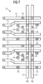
- FIGS. 7 and 8 show two exemplary embodiments for a DRAM memory layout 70 which have a correspondingly optimized architecture of the bit lines 71.
- Both DRAM memories 70 have a number of memory cells which are designed as 6 F 2 memory cells.
- the contacts 73 between the bit lines 71 and the DRAM memory cells are represented by crossed boxes.
- the contacts 74 between the metal word line 72 and the respective poly islands are shown as squares with a circle.
- Bit lines 71 laid so that at least one decency each observed between the individual elements of 1 F. becomes. As a result, some of the bit lines 71 have offsets exhibit.
- the distance between the bit lines 71 and contacts 74 reduced to 1 ⁇ 2 F, as shown in Figure 8 is shown, the bit lines 71 can be identical Raster just over the memory cell array of the DRAM memory be relocated.
Landscapes
- Engineering & Computer Science (AREA)
- Microelectronics & Electronic Packaging (AREA)
- Computer Hardware Design (AREA)
- Semiconductor Memories (AREA)
Abstract
Description
Claims (17)
- Integrierte DRAM-Speicherzelle, mit einem Speicherkondensator (11; 52) und einem Auswahltransistor (12), die im Bereich einer zumindest im wesentlichen rechteckigen Zellfläche (20; 59) ausgebildet sind, wobei die Zellfläche (20; 59) eine größere Ausdehnung in Längsrichtung (L) als in Breitenrichtung (B) aufweist, und die über eine Wortleitung (16, 17; 56, 57) und eine Bitleitung (15; 55) mit der Zellperipherie (18) verdrahtet oder verdrahtbar ist, wobei die Wortleitung (16, 17; 56, 57) und die Bitleitung (15; 55) über die Speicherzelle (10; 51) geführt und zumindest im wesentlichen senkrecht zueinander orientiert sind,
dadurch gekennzeichnet, daß die Bitleitung (15; 55) senkrecht zur Längsausdehnung (21) der Speicherzelle (10; 51) in Richtung der Breitenausdehnung (22) der Speicherzelle (10; 51) orientiert ist. - DRAM-Speicher nach Anspruch 1,
dadurch gekennzeichnet, daß diese eine Zellfläche (20; 59) von < 8 F2 aufweist. - DRAM-Speicherzelle nach Anspruch 1 oder 2,
dadurch gekennzeichnet, daß die Bitleitung (15; 55) und/oder die Wortleitung(en) (16, 17; 56, 57) eine Breite von 1 F aufweist/aufweisen. - DRAM-Speicherzelle nach einem der Ansprüche 1 bis 3,
dadurch gekennzeichnet, daß diese eine Zellbreite (22) von 2 F aufweist. - DRAM-Speicherzelle nach einem der Ansprüche 1 bis 4,
dadurch gekennzeichnet, daß diese eine Zellenlänge (21) von < 4 F aufweist. - DRAM-Speicher, mit einer Anzahl von Speicherzellen (10; 51) nach einem der Ansprüche 1 bis 5, die jeweils ein oder mehrere Speicherzellenfelder (31) bilden, wobei jeweils mehrere Speicherzellen (10; 51) eines Speicherzellenfeldes (31) mit einer Wortleitung (16, 17; 56, 57) und einer Bitleitung (32, 33; 55) verbunden sind, wobei die Wortleitungen (16, 17; 56, 57) ein Wortleitungsraster und die Bitleitungen (32, 33; 55) ein Bitleitungsraster bilden.
- DRAM-Speicher nach Anspruch 6,
dadurch gekennzeichnet, daß diese eine "open" Struktur aufweist. - DRAM-Speicher nach Anspruch 7,
dadurch gekennzeichnet, daß als Referenz-Bitleitung (33) für die Bitleitung (32; 55) einer Speicherzelle (10; 51) eine Bitleitung (33; 55) aus einem anderen Speicherzellenfeld (31) verwendet wird. - DRAM-Speicher nach einem der Ansprüche 6 bis 8,
dadurch gekennzeichnet, daß das Bitleitungsraster als Funktion der Längsausdehnung (21) der Speicherzellen (10; 51) gebildet ist. - DRAM-Speicher nach einem der Ansprüche 6 bis 9,
dadurch gekennzeichnet, daß dieser einen oder mehrere Schreib-Leseverstärker (34) aufweist, der/die zur Auswertung und Weiterverarbeitung der über die Bitleitung (32, 33; 55) übertragenen Signale mit diesen verdrahtet ist/sind. - DRAM-Speicher nach Anspruch 10,
dadurch gekennzeichnet, daß die Schreib-Leseverstärker (34) in einem zum Bitleitungsraster korrespondierenden Raster angeordnet sind, so daß das Raster der Schreib-Leseverstärker (34) linear mit der Längsausdehnung (21) der Speicherzellen (10; 51) skaliert. - DRAM-Speicher nach einem der Ansprüche 6 bis 11,
dadurch gekennzeichnet, daß jeweils mehrere Gates (60), insbesondere vier Gates, benachbarter Speicherzellen (10; 51) inselartig über eine Wortleitung (57) miteinander verbunden sind. - DRAM-Speicher nach Anspruch 12,
dadurch gekennzeichnet, daß die Wortleitung (57) als Polysiliziumleitung ausgebildet ist. - DRAM-Speicher nach Anspruch 12 oder 13,
dadurch gekennzeichnet, daß die Wortleitung (57) in bestimmten Abständen mit einer Metall-Wortleitung (56) verbunden ist. - DRAM-Speicher nach Anspruch 14,
dadurch gekennzeichnet, daß die Wortleitungen (56, 57) übereinander angeordnet sind. - DRAM-Speicher nach Anspruch 14 oder 15,
dadurch gekennzeichnet, daß zwei nebeneinander laufende Metall-Wortleitungen (56) wechselseitig jeweils Speicherzellen-Gates (60) verschiedenen Typs kontaktieren. - DRAM-Speicher nach einem der Ansprüche 12 bis 16,
dadurch gekennzeichnet, daß die, benachbarte Speicherzellen (10; 51) inselartig verbindende, Wortleitung (57) über das Source-Drain-Gebiet der Speicherzelle(n) (10; 51) geführt ist, das den Speicherkondensator (11; 52) mit dem Auswahltransistor (12) verbindet.
Applications Claiming Priority (2)
| Application Number | Priority Date | Filing Date | Title |
|---|---|---|---|
| DE10011672 | 2000-03-10 | ||
| DE10011672A DE10011672A1 (de) | 2000-03-10 | 2000-03-10 | Integrierte DRAM-Speicherzelle sowie DRAM-Speicher |
Publications (2)
| Publication Number | Publication Date |
|---|---|
| EP1132966A2 true EP1132966A2 (de) | 2001-09-12 |
| EP1132966A3 EP1132966A3 (de) | 2007-10-03 |
Family
ID=7634209
Family Applications (1)
| Application Number | Title | Priority Date | Filing Date |
|---|---|---|---|
| EP01105390A Withdrawn EP1132966A3 (de) | 2000-03-10 | 2001-03-09 | Bit- und Wortleitungsanordnung für DRAM-Speicher |
Country Status (5)
| Country | Link |
|---|---|
| US (1) | US6445609B2 (de) |
| EP (1) | EP1132966A3 (de) |
| JP (1) | JP4063502B2 (de) |
| KR (1) | KR100437143B1 (de) |
| DE (1) | DE10011672A1 (de) |
Cited By (1)
| Publication number | Priority date | Publication date | Assignee | Title |
|---|---|---|---|---|
| CN1315192C (zh) * | 2001-11-20 | 2007-05-09 | 松下电器产业株式会社 | 半导体记忆装置 |
Families Citing this family (1)
| Publication number | Priority date | Publication date | Assignee | Title |
|---|---|---|---|---|
| CN121152201A (zh) * | 2024-06-13 | 2025-12-16 | 北京超弦存储器研究院 | 一种存储器及其访问方法、电子设备 |
Family Cites Families (13)
| Publication number | Priority date | Publication date | Assignee | Title |
|---|---|---|---|---|
| JPS55150267A (en) * | 1979-05-10 | 1980-11-22 | Fujitsu Ltd | Semiconductor memory cell |
| JPS60136365A (ja) * | 1983-12-26 | 1985-07-19 | Hitachi Ltd | 半導体装置 |
| JPH0815208B2 (ja) * | 1987-07-01 | 1996-02-14 | 三菱電機株式会社 | 半導体記憶装置 |
| JP2682021B2 (ja) * | 1988-06-29 | 1997-11-26 | 富士通株式会社 | 半導体メモリ装置 |
| JP2572864B2 (ja) * | 1990-02-01 | 1997-01-16 | 三菱電機株式会社 | 半導体装置の製造方法 |
| JP3126739B2 (ja) * | 1990-12-06 | 2001-01-22 | 三菱電機株式会社 | 半導体記憶装置およびその製造方法 |
| DE4123209A1 (de) * | 1991-07-12 | 1993-01-14 | Siemens Ag | Gaslaser |
| KR950011636B1 (ko) * | 1992-03-04 | 1995-10-07 | 금성일렉트론주식회사 | 개선된 레이아웃을 갖는 다이내믹 랜덤 액세스 메모리와 그것의 메모리셀 배치방법 |
| JP2824713B2 (ja) * | 1992-04-24 | 1998-11-18 | 三菱電機株式会社 | 半導体記憶装置 |
| JPH07202022A (ja) * | 1993-12-28 | 1995-08-04 | Nippon Steel Corp | 半導体記憶装置 |
| DE19519160C1 (de) * | 1995-05-24 | 1996-09-12 | Siemens Ag | DRAM-Zellenanordnung und Verfahren zu deren Herstellung |
| KR0165406B1 (ko) * | 1995-06-26 | 1998-12-15 | 김광호 | 에스 렘 셀 |
| US5817522A (en) | 1997-11-12 | 1998-10-06 | Goodman; David B. P. | Self-contained assay device and method |
-
2000
- 2000-03-10 DE DE10011672A patent/DE10011672A1/de not_active Withdrawn
-
2001
- 2001-03-08 KR KR10-2001-0012062A patent/KR100437143B1/ko not_active Expired - Fee Related
- 2001-03-09 US US09/801,715 patent/US6445609B2/en not_active Expired - Lifetime
- 2001-03-09 EP EP01105390A patent/EP1132966A3/de not_active Withdrawn
- 2001-03-12 JP JP2001068253A patent/JP4063502B2/ja not_active Expired - Fee Related
Cited By (1)
| Publication number | Priority date | Publication date | Assignee | Title |
|---|---|---|---|---|
| CN1315192C (zh) * | 2001-11-20 | 2007-05-09 | 松下电器产业株式会社 | 半导体记忆装置 |
Also Published As
| Publication number | Publication date |
|---|---|
| JP4063502B2 (ja) | 2008-03-19 |
| EP1132966A3 (de) | 2007-10-03 |
| DE10011672A1 (de) | 2001-09-20 |
| KR20010089224A (ko) | 2001-09-29 |
| KR100437143B1 (ko) | 2004-06-25 |
| US6445609B2 (en) | 2002-09-03 |
| US20010036102A1 (en) | 2001-11-01 |
| JP2001291848A (ja) | 2001-10-19 |
Similar Documents
| Publication | Publication Date | Title |
|---|---|---|
| DE4433695C2 (de) | Dynamische Halbleiterspeichervorrichtung | |
| DE3915438C2 (de) | ||
| DE69121760T2 (de) | Halbleiterspeicherzelle | |
| DE3222461C2 (de) | ||
| DE3941926C2 (de) | Halbleiterspeichereinrichtung | |
| DE10196802B4 (de) | Rauschunterdrückung für DRAM-Architekturen mit offener Bitleitung | |
| DE69822280T2 (de) | Halbleiterspeicher | |
| DE10123514B4 (de) | Halbleiter-Speicherbaustein | |
| DE3937068C2 (de) | Dynamische Halbleiterspeicheranordnung | |
| DE4024295C2 (de) | Dynamische Halbleiterspeichervorrichtung | |
| DE4000429C2 (de) | Dram | |
| DE19832994C2 (de) | Ferroelektrische Speicheranordnung | |
| DE10334424A1 (de) | Halbleiterspeichervorrichtung mit Doppelzelleneinheiten | |
| DE102012019196A1 (de) | Speicherarray mit hierarchischer Bitleitungsstruktur | |
| DE69604078T2 (de) | Verflochtenen belegungskonfiguration für verbundenen differentiellenpaarleitungen | |
| DE4406459C2 (de) | Integrierte Halbleiterschaltungsvorrichtung mit Speicherzellenanordnung | |
| DE69225298T2 (de) | Halbleiterspeichervorrichtung | |
| DE69722132T2 (de) | Statische Halbleiterspeicheranordnung mit Vorausladungsschaltung mit ähnlicher Konfiguration wie Speicherzelle | |
| DE102004021051B3 (de) | DRAM-Speicherzellenanordnung nebst Betriebsverfahren | |
| DE2642615A1 (de) | Halbleiterspeicher | |
| DE102004062451A1 (de) | Halbleiterspeicherbauelement mit verschränkten Leitungen, Leitungsentwurfsstruktur und Leitungsentwurfsverfahren | |
| DE60118833T2 (de) | Halbleiter-Speicher mit unterteilter Wortleitungstruktur | |
| DE10009346A1 (de) | Schreib-/Leseverstärker mit Vertikaltransistoren für DRAM-Speicher | |
| EP1132966A2 (de) | Bit- und Wortleitungsanordnung für DRAM-Speicher | |
| DE102005046777B4 (de) | Halbleiterspeicher-Einrichtung |
Legal Events
| Date | Code | Title | Description |
|---|---|---|---|
| PUAI | Public reference made under article 153(3) epc to a published international application that has entered the european phase |
Free format text: ORIGINAL CODE: 0009012 |
|
| AK | Designated contracting states |
Kind code of ref document: A2 Designated state(s): AT BE CH CY DE DK ES FI FR GB GR IE IT LI LU MC NL PT SE TR |
|
| AX | Request for extension of the european patent |
Free format text: AL;LT;LV;MK;RO;SI |
|
| PUAL | Search report despatched |
Free format text: ORIGINAL CODE: 0009013 |
|
| AK | Designated contracting states |
Kind code of ref document: A3 Designated state(s): AT BE CH CY DE DK ES FI FR GB GR IE IT LI LU MC NL PT SE TR |
|
| AX | Request for extension of the european patent |
Extension state: AL LT LV MK RO SI |
|
| 17P | Request for examination filed |
Effective date: 20071204 |
|
| AKX | Designation fees paid |
Designated state(s): DE |
|
| 17Q | First examination report despatched |
Effective date: 20090429 |
|
| STAA | Information on the status of an ep patent application or granted ep patent |
Free format text: STATUS: THE APPLICATION IS DEEMED TO BE WITHDRAWN |
|
| 18D | Application deemed to be withdrawn |
Effective date: 20090910 |