EP1116008B1 - Gyrometre vibrant et son procede de fabrication - Google Patents
Gyrometre vibrant et son procede de fabrication Download PDFInfo
- Publication number
- EP1116008B1 EP1116008B1 EP99946323A EP99946323A EP1116008B1 EP 1116008 B1 EP1116008 B1 EP 1116008B1 EP 99946323 A EP99946323 A EP 99946323A EP 99946323 A EP99946323 A EP 99946323A EP 1116008 B1 EP1116008 B1 EP 1116008B1
- Authority
- EP
- European Patent Office
- Prior art keywords
- wafer
- insulating layer
- ring element
- gyrometer
- portions
- Prior art date
- Legal status (The legal status is an assumption and is not a legal conclusion. Google has not performed a legal analysis and makes no representation as to the accuracy of the status listed.)
- Expired - Lifetime
Links
- 238000000034 method Methods 0.000 title claims abstract description 166
- 238000004519 manufacturing process Methods 0.000 title claims abstract description 21
- 230000008569 process Effects 0.000 title claims description 64
- 238000005530 etching Methods 0.000 claims abstract description 44
- 238000000059 patterning Methods 0.000 claims abstract description 4
- 235000012431 wafers Nutrition 0.000 claims description 285
- 239000000463 material Substances 0.000 claims description 85
- 210000003041 ligament Anatomy 0.000 claims description 28
- 239000013078 crystal Substances 0.000 claims description 26
- 150000004767 nitrides Chemical class 0.000 claims description 23
- 230000010355 oscillation Effects 0.000 claims description 16
- 230000033001 locomotion Effects 0.000 claims description 15
- 239000003990 capacitor Substances 0.000 claims description 14
- 239000000945 filler Substances 0.000 claims description 8
- 238000006073 displacement reaction Methods 0.000 claims description 7
- 238000004140 cleaning Methods 0.000 claims description 5
- 230000008859 change Effects 0.000 claims description 4
- 239000002178 crystalline material Substances 0.000 claims description 4
- 239000000758 substrate Substances 0.000 claims description 4
- 230000000737 periodic effect Effects 0.000 claims description 3
- 239000010703 silicon Substances 0.000 abstract description 81
- 229910052710 silicon Inorganic materials 0.000 abstract description 80
- 238000005516 engineering process Methods 0.000 abstract description 8
- 239000012212 insulator Substances 0.000 abstract description 8
- 239000010410 layer Substances 0.000 description 252
- XUIMIQQOPSSXEZ-UHFFFAOYSA-N Silicon Chemical compound [Si] XUIMIQQOPSSXEZ-UHFFFAOYSA-N 0.000 description 78
- 230000008901 benefit Effects 0.000 description 22
- 238000005334 plasma enhanced chemical vapour deposition Methods 0.000 description 19
- 238000000623 plasma-assisted chemical vapour deposition Methods 0.000 description 19
- 238000012545 processing Methods 0.000 description 19
- 230000001965 increasing effect Effects 0.000 description 18
- 239000003550 marker Substances 0.000 description 13
- 230000000694 effects Effects 0.000 description 10
- 238000005498 polishing Methods 0.000 description 10
- 239000003795 chemical substances by application Substances 0.000 description 9
- 229910021420 polycrystalline silicon Inorganic materials 0.000 description 8
- 239000011800 void material Substances 0.000 description 8
- 239000002019 doping agent Substances 0.000 description 7
- 238000001312 dry etching Methods 0.000 description 7
- 229920005591 polysilicon Polymers 0.000 description 7
- 239000000126 substance Substances 0.000 description 7
- VYPSYNLAJGMNEJ-UHFFFAOYSA-N Silicium dioxide Chemical compound O=[Si]=O VYPSYNLAJGMNEJ-UHFFFAOYSA-N 0.000 description 6
- 238000002120 advanced silicon etching Methods 0.000 description 6
- 230000035945 sensitivity Effects 0.000 description 6
- 230000008719 thickening Effects 0.000 description 6
- 239000004642 Polyimide Substances 0.000 description 5
- 238000013461 design Methods 0.000 description 5
- 239000007788 liquid Substances 0.000 description 5
- 230000000873 masking effect Effects 0.000 description 5
- 238000005459 micromachining Methods 0.000 description 5
- 229920001721 polyimide Polymers 0.000 description 5
- 230000009286 beneficial effect Effects 0.000 description 4
- 239000004020 conductor Substances 0.000 description 4
- 238000000151 deposition Methods 0.000 description 4
- BHEPBYXIRTUNPN-UHFFFAOYSA-N hydridophosphorus(.) (triplet) Chemical compound [PH] BHEPBYXIRTUNPN-UHFFFAOYSA-N 0.000 description 4
- 239000012071 phase Substances 0.000 description 4
- YCKRFDGAMUMZLT-UHFFFAOYSA-N Fluorine atom Chemical compound [F] YCKRFDGAMUMZLT-UHFFFAOYSA-N 0.000 description 3
- 238000009835 boiling Methods 0.000 description 3
- 229910052731 fluorine Inorganic materials 0.000 description 3
- 239000011737 fluorine Substances 0.000 description 3
- 238000000227 grinding Methods 0.000 description 3
- 150000002500 ions Chemical class 0.000 description 3
- 238000004518 low pressure chemical vapour deposition Methods 0.000 description 3
- 238000001465 metallisation Methods 0.000 description 3
- 229920002120 photoresistant polymer Polymers 0.000 description 3
- 238000001020 plasma etching Methods 0.000 description 3
- 229920000642 polymer Polymers 0.000 description 3
- 230000009467 reduction Effects 0.000 description 3
- 229910021332 silicide Inorganic materials 0.000 description 3
- 229910052814 silicon oxide Inorganic materials 0.000 description 3
- 238000010561 standard procedure Methods 0.000 description 3
- 239000000725 suspension Substances 0.000 description 3
- 239000013077 target material Substances 0.000 description 3
- ZOXJGFHDIHLPTG-UHFFFAOYSA-N Boron Chemical compound [B] ZOXJGFHDIHLPTG-UHFFFAOYSA-N 0.000 description 2
- 229910052581 Si3N4 Inorganic materials 0.000 description 2
- 229910052787 antimony Inorganic materials 0.000 description 2
- WATWJIUSRGPENY-UHFFFAOYSA-N antimony atom Chemical compound [Sb] WATWJIUSRGPENY-UHFFFAOYSA-N 0.000 description 2
- 229910052785 arsenic Inorganic materials 0.000 description 2
- RQNWIZPPADIBDY-UHFFFAOYSA-N arsenic atom Chemical compound [As] RQNWIZPPADIBDY-UHFFFAOYSA-N 0.000 description 2
- 238000010420 art technique Methods 0.000 description 2
- 229910052796 boron Inorganic materials 0.000 description 2
- 230000008878 coupling Effects 0.000 description 2
- 238000010168 coupling process Methods 0.000 description 2
- 238000005859 coupling reaction Methods 0.000 description 2
- 230000001419 dependent effect Effects 0.000 description 2
- 230000008021 deposition Effects 0.000 description 2
- 238000005137 deposition process Methods 0.000 description 2
- 239000003814 drug Substances 0.000 description 2
- 229910052732 germanium Inorganic materials 0.000 description 2
- GNPVGFCGXDBREM-UHFFFAOYSA-N germanium atom Chemical compound [Ge] GNPVGFCGXDBREM-UHFFFAOYSA-N 0.000 description 2
- 238000009616 inductively coupled plasma Methods 0.000 description 2
- 238000003331 infrared imaging Methods 0.000 description 2
- 230000037361 pathway Effects 0.000 description 2
- 238000007517 polishing process Methods 0.000 description 2
- 239000000377 silicon dioxide Substances 0.000 description 2
- 235000012239 silicon dioxide Nutrition 0.000 description 2
- HQVNEWCFYHHQES-UHFFFAOYSA-N silicon nitride Chemical compound N12[Si]34N5[Si]62N3[Si]51N64 HQVNEWCFYHHQES-UHFFFAOYSA-N 0.000 description 2
- 238000009966 trimming Methods 0.000 description 2
- 238000001039 wet etching Methods 0.000 description 2
- BOTDANWDWHJENH-UHFFFAOYSA-N Tetraethyl orthosilicate Chemical compound CCO[Si](OCC)(OCC)OCC BOTDANWDWHJENH-UHFFFAOYSA-N 0.000 description 1
- 230000001133 acceleration Effects 0.000 description 1
- 230000004075 alteration Effects 0.000 description 1
- 238000004873 anchoring Methods 0.000 description 1
- 238000000137 annealing Methods 0.000 description 1
- 230000004888 barrier function Effects 0.000 description 1
- 230000015572 biosynthetic process Effects 0.000 description 1
- 238000003486 chemical etching Methods 0.000 description 1
- 238000005229 chemical vapour deposition Methods 0.000 description 1
- 238000010276 construction Methods 0.000 description 1
- 229910021419 crystalline silicon Inorganic materials 0.000 description 1
- 238000012938 design process Methods 0.000 description 1
- 238000001514 detection method Methods 0.000 description 1
- 229910003460 diamond Inorganic materials 0.000 description 1
- 239000010432 diamond Substances 0.000 description 1
- 238000001035 drying Methods 0.000 description 1
- 230000007613 environmental effect Effects 0.000 description 1
- 238000003384 imaging method Methods 0.000 description 1
- 230000006872 improvement Effects 0.000 description 1
- 238000011065 in-situ storage Methods 0.000 description 1
- 238000010348 incorporation Methods 0.000 description 1
- 230000001939 inductive effect Effects 0.000 description 1
- 230000010354 integration Effects 0.000 description 1
- 238000010884 ion-beam technique Methods 0.000 description 1
- 239000007791 liquid phase Substances 0.000 description 1
- 239000012528 membrane Substances 0.000 description 1
- 238000004377 microelectronic Methods 0.000 description 1
- 238000012856 packing Methods 0.000 description 1
- 230000003071 parasitic effect Effects 0.000 description 1
- 230000004044 response Effects 0.000 description 1
- 238000001878 scanning electron micrograph Methods 0.000 description 1
- 239000004065 semiconductor Substances 0.000 description 1
- FVBUAEGBCNSCDD-UHFFFAOYSA-N silicide(4-) Chemical compound [Si-4] FVBUAEGBCNSCDD-UHFFFAOYSA-N 0.000 description 1
- 239000002210 silicon-based material Substances 0.000 description 1
- 238000004611 spectroscopical analysis Methods 0.000 description 1
- 239000010421 standard material Substances 0.000 description 1
- 239000002344 surface layer Substances 0.000 description 1
- 230000026683 transduction Effects 0.000 description 1
- 238000010361 transduction Methods 0.000 description 1
- 238000007514 turning Methods 0.000 description 1
- XLYOFNOQVPJJNP-UHFFFAOYSA-N water Substances O XLYOFNOQVPJJNP-UHFFFAOYSA-N 0.000 description 1
- 238000009736 wetting Methods 0.000 description 1
Images


Classifications
-
- H—ELECTRICITY
- H01—ELECTRIC ELEMENTS
- H01L—SEMICONDUCTOR DEVICES NOT COVERED BY CLASS H10
- H01L29/00—Semiconductor devices adapted for rectifying, amplifying, oscillating or switching, or capacitors or resistors with at least one potential-jump barrier or surface barrier, e.g. PN junction depletion layer or carrier concentration layer; Details of semiconductor bodies or of electrodes thereof ; Multistep manufacturing processes therefor
- H01L29/66—Types of semiconductor device ; Multistep manufacturing processes therefor
- H01L29/84—Types of semiconductor device ; Multistep manufacturing processes therefor controllable by variation of applied mechanical force, e.g. of pressure
-
- G—PHYSICS
- G01—MEASURING; TESTING
- G01C—MEASURING DISTANCES, LEVELS OR BEARINGS; SURVEYING; NAVIGATION; GYROSCOPIC INSTRUMENTS; PHOTOGRAMMETRY OR VIDEOGRAMMETRY
- G01C19/00—Gyroscopes; Turn-sensitive devices using vibrating masses; Turn-sensitive devices without moving masses; Measuring angular rate using gyroscopic effects
- G01C19/56—Turn-sensitive devices using vibrating masses, e.g. vibratory angular rate sensors based on Coriolis forces
Definitions
- This invention relates to improvements in manufacturing gyrometers.
- GB 2 276 976 shows a particular method for the production of such a sensor wherein a silicon wafer has cavities formed into its surface. Next a second wafer is bonded to the surface of the first wafer and the second wafer etched in a manner to release portions of the second wafer which are above the cavities in the first wafer. Thus, suspended resonating portions are formed which exist above the cavities in the first wafer.
- WO 95/08775 shows a structure wherein a layer of silicon is formed onto a substrate. The silicon is etched in a manner to form suspended resonator portions above cavities in the silicon.
- micro-mechanical sensor is the vibratory gyrometer which measures the rate of turn and has applications in the fields of vehicle control, smart munitions, robotics, virtual reality, leisure and medicine as well as other fields.
- JP09145740 describes an acceleration sensor having a sensor electrode that is shaped to overcome effects associated with the in-plane anisotropy of the material from which it is formed.
- the present invention relates to a micro- mechanical ring gyrometer and its fabrication method.
- a micro-mechanical ring gyrometer comprising a ring element fabricated from a material having anisotropic mechanical properties characterised in that the ring element is arranged to oscillate during use and in that at least one region of the ring element is thickened relative to the remainder of the ring element to substantially compensate for the anisotropic mechanical properties of the material from which the ring element is fabricated.
- the dimensions of at least a portion of the ring element may be thicker or thinner in a periodic manner when compared to the remainder of the element.
- the gyrometer may function as if it were fabricated from an isotropic material. This has the advantage that material showing imperfect properties can be used to fabricate the gyrometer and yet the gyrometer will still function accurately.
- Such gyrometers have a number of applications including: vehicle control, smart munitions, robotics, virtual reality and medicine.
- the gyrometer is fabricated from an anisotropic material. This is advantageous because this can be substantially cheaper than isotropic material.
- the gyrometer is fabricated from silicon with the lattice spacing of substantially ⁇ 100> as the plane of the silicon wafer. It is known that within ⁇ 100> silicon the modulus of rigidity and the radial Young's modulus vary significantly in a cos4 ⁇ manner (where ⁇ is an angle within a plane in the silicon from a reference point on that plane).
- Previously micro-mechanical gyrometers have been fabricated from silicon wafers with substantially ⁇ 111> as the plane of the wafer. In such ⁇ 111> oriented silicon the radial Young's modulus varies little with angular orientation. As the skilled person will appreciate ⁇ 111> silicon is more expensive than ⁇ 100> silicon and it is therefore advantageous to be able to use ⁇ 100> silicon. However, until the realisation of this invention it was not possible to use ⁇ 100> silicon without employing tuning methods (for example laser trimming) because the anisotropic nature of the material led to inaccurate performance of the gyrometer. Using ⁇ 100> silicon materials may also make integration of on chip electronics simpler, and hence improve performance.
- the gyrometer has a number of sensing elements e.g. 8 or 16 or 32 or 64 or 128 sensing elements.
- the sensing elements may be equispaced around a circle, e.g. when eight sensing elements are provided these may be arranged at 45° intervals around the circle.
- the gyrometer is fabricated from a ring and may be supported by suspension elements / ligaments with at least eight sensing elements which may be arranged at 45° intervals around a circle. If such a gyrometer (having drive and sense modes) were fabricated from ⁇ 100> silicon with all of the sensing elements of equal dimensions the effect of the anisotropy would be to cause a split in the frequencies of the drive and sense modes. This split is significant and causes a reduction in gyrometer sensitivity as the modes do not efficiently couple under an applied rate of turn and high levels of mechanical coupling swamp the sense signal.
- sensing elements When eight sensing elements are provided, four of these may have a portion of increased thickness when compared with the remaining four sensing elements.
- One embodiment would be to thicken portions of the ring associated with alternative sensing elements when compared to the remaining portions of the ring. This thickening may be an approximation to a cos4 ⁇ variation, or may be substantially a cos4 ⁇ variation.
- the sensing elements having a portion of increased thickness may be thickened when compared to the remaining sensing elements by an amount substantially in the range 0.1 ⁇ m to 50 ⁇ m, e.g. 13 ⁇ m.
- the required thickening of the elements will vary according to the dimensions of the wafer and size of device. For a 100 ⁇ m thick ring the portion of increased thickness may be thickened when compared to the remaining portions of the ring by substantially 13 ⁇ m. However, this thickening is merely an indication since the precise increase needs to be calculated for each particular design. Other stages may be thickened to account for anisotropy in ⁇ 100> silicon.
- the sensing elements may be provided in pairs with one sensing element of each pair being provided on one side of the ring element and the other sensing element being provided on the other. Such a structure is advantageous because it may provide an increased performance over providing single sensing elements on a single side of the ring.
- the ring element forms a capacitive plate and the sensing elements other capacitive plates.
- the arrangement may form a differential capacitor pair with the ring element as a common plate (or electrode), and the sensing elements (electrodes) the other plate in each capacitor. This structure allows changes of capacitance to be measured as the ring element moves providing a convenient structure, and way of obtaining readings from the gyrometer.
- suspension ligaments are provided on an inside region of the ring element and in other embodiments the suspension ligaments are provided on an outside region of the ring element. Both of these arrangements provide a convenient structure for supporting the ring.
- Voltages applied to the sensing elements may be adapted to nullify a particular mode of oscillation of the ring element. Again this may lead to improved performance of the gyrometer.
- the skilled person will appreciate that the gyrometer is driven so that the ring element oscillates at a first harmonic and that an applied rate of turn induces a second harmonic which is generally at 45° to the first. It may be the second harmonic which is adapted to be nullified.
- a closed loop control means may be provided to monitor and control the amplitude of the oscillation of the second harmonic.
- An advantage of such an arrangement is that noise common to both sensing elements can be rejected (common mode noise rejection is increased) and therefore the performance of the gyrometer may be increased.
- the sensing elements which are differentially connected to the processing means may be spaced around the ring element.
- the sensing elements may be provided in a pair with the ring element passing between the pair.
- the processing means may comprise signal processing and control circuitry.
- the method may comprise applying voltages to one or more of the sensing elements, thus providing a way of controlling displacement of the ring element.
- the method may comprise applying voltages such that displacement of portions of the ring element are substantially prevented. As discussed hereinbefore a rate of turn induces a secondary harmonic in the oscillations of the ring element.
- the method may comprise applying a voltage to substantially prevent the ring from oscillating at the secondary harmonic.
- the method comprises applying voltages to the sensing elements such that the ring element is made to function as if it were fabricated from a material having isotropic properties (which may be ⁇ 111> silicon).
- the method may comprise applying voltages substantially in anti-phase to each element of the pair. This has the advantage that stronger forces are applied to the ring element.
- a method of fabricating a micro-mechanical ring gyrometer comprising steps of; (i) taking a layer of crystalline material having anisotropic mechanical properties and (ii) determining the degree of mis-alignment of the crystal lattice within said layer of material by identifying the exact crystal orientation characterised in that the method further comprises the steps of (iii) calculating the degree of change required in the thickness dimension of a ring element formed in the layer of crystalline material to compensate for the misalignment of the crystal lattice; and (iv) fabricating such a ring element in said layer of material wherein at least one region of the ring element is thickened relative to the remainder of the ring element to substantially compensate for said mis-alignment and hence the anisotropic mechanical properties of said layer of material.
- the step of fabricating the ring element of the invention comprises taking a first wafer with an insulating layer formed thereon and with a second wafer bonded to the insulating layer and
- the micro-mechanical sensor so formed comprises both suspended portions and also portions anchored to the other wafer by the insulating layer.
- etchants will generally etch any free surfaces of a target material which they contact. Therefore, if a volume of target material is exposed to an etchant it will be etched from each of the sides which the etchant contacts. The length of time it takes the etchant to completely remove the target material will depend upon the shortest distance from an edge portion of the volume to the centre of the volume. Thus a long thin shape will be remove before a square shape of equal volume. Thus, the predetermined size above which suspended portions become separated from the other wafer depends upon the dimensions of the volume of the insulating layer being etched.
- Step b) of the process may be performed in a single pattern and etch step or may be as a series of pattern and etch steps.
- the insulating layer may be thought of as a sacrificial layer and as an anchoring layer. However, the skilled person will appreciate that the insulating layer has insulating properties which may be utilised.
- SSM sacrificial surface micro-machining
- TBM bulk micro-machining
- structures formed in the etched wafer can be made with a greater depth than in prior art methods using surface micromachining (SSM) wherein layers are deposited or other types of Silicon On Insulator processing.
- SSM surface micromachining
- Typical depth limits for a deposited layer are between 10 ⁇ m-20 ⁇ m. It would not have been possible to reliably deposit material to the depth achieved by the present method. For instance providing material by deposition has the problem that the uniformity of the material is hard to control with errors of 5% across a wafer being typical. Further, the process provides a buried insulating layer.
- the present method may be used to fabricate structures having a depth of up to substantially 2mm. Possibly this may be increased to 2.5mm, 3mm, 3.5mm or 4mm.
- wafers can be purchased which comply with the starting steps of the method; that is a sandwich structure of two wafers with an insulating layer provided between them. Therefore, the starting point in the process may be the commercially available sandwich structure.
- the method may however, include the steps of fabricating an insulating layer onto a first wafer and subsequently bonding the second wafer to the insulating layer.
- the cost of a wafer with silicon and insulating layers provided on the surface is higher than the cost of a wafer without the extra layers provided.
- the combined advantages of the invention may more than offset the higher cost of the wafer with the extra layers compared to a standard wafer.
- the gap between the suspended portions defined from said one layer and said other wafer is defined by the thickness of the insulating layer and therefore by controlling the thickness of the insulating layer between the first and second wafers this gap may be controlled.
- the thickness of the insulating layer may be substantially in the range 10 nm to 20 ⁇ m. More preferably the insulating layer has a thickness substantially in the range 100 nm to 10 ⁇ m. In the most preferred embodiments the thickness lies substantially in the range 1 ⁇ m to 5 ⁇ m. In particular, layer thickness of substantially 1.5 ⁇ m and 3 ⁇ m may be suitable.
- the first wafer is a mechanical wafer which undergoes subsequent processing to have the structure formed therein.
- An advantage of forming the insulating layer on the mechanical wafer is that a cleaner interface is formed for subsequent processing (for example etching).
- a further advantage of providing the first wafer as the mechanical wafer is that the devices subsequently formed from the mechanical wafer are formed from the single crystal structure of the wafer.
- this has advantages, namely it is likely that devices formed will have a higher reliability and that resonant devices formed will have a higher quality factor when compared to structures formed in polycrystalline materials of prior art methods.
- the single crystal of the wafer often shows anisotropic properties and considerations may arise which need to be considered in the design stage to account for the anisotropic nature.
- the anisotropic properties may depend on factors including crystal orientation of the material and the accuracy of any cut of the crystal.
- the second wafer is a substrate or handle wafer which is provided as a support for the micro-mechanical sensor.
- the first wafer may be a substrate or handle wafer and the second wafer may be a mechanical wafer which undergoes subsequent processing (for example etching).
- subsequent processing for example etching
- One company capable of providing a sandwich structure capable of being used for the start of the method is BCO Technologies (NI) Ltd., Harbor, BT 11 8BU.
- the method may comprise an additional step of polishing the wafer to be etched (which may be either the first or second wafer) to the desired thickness.
- This polishing may be performed as part of bonding the second wafer to the insulating layer or as an additional step before step a) of the method is performed.
- This has the advantage that the micro-mechanical sensor so formed by the method can be tailored to the correct thickness.
- the polishing may be performed by mechanical means (for instance grinding), or may be by chemical means (for instance etching) or may be by a combination of mechanical and chemical means.
- An advantage of the present method is that the wafer being polished is supported over its entire area by a combination of the other wafer and the insulating layer. In some prior art methods a wafer which was not supported over its entire area was polished which in some instances led to buckling of the wafer over the unsupported areas.
- wet chemical etchants may be used to etch the channels into the etched wafer and isotropic or anisotropic profiles may be provided.
- dry etching may be used. Such etching is advantageous because it increases the aspect ratio of depth to width which can be achieved by using wet etching. Also, the minimum feature size may be reduced and density of features may be increased using dry etching.
- a deep dry etcher such as an advanced silicon etch (ASE) system produced by Surface Technology Systems using a fluorine based inductively coupled plasma may be used.
- ASE advanced silicon etch
- packing density may be increased by the use of dry etching over that for wet processes associated with TBM which may reduce unit costs.
- the mask for the etch of step a) is optimised so that the areas to be etched have substantially equal cross sectional areas and pattern density. This may be important should a deep dry etcher be used; the rate of etch for such a system is dependent on cross sectional area and pattern density and therefore should regions having different cross sectional areas or pattern densities be used they will etch at different rates.
- the method includes providing suspensory ligaments between the suspended portions and the remainder of the etched wafer.
- These suspensory ligaments have the advantage that when the suspended portions are released from the other wafer (by the removal of the insulating layer) they are maintained in situ by the suspensory ligament.
- the suspensory ligaments may comprise portions of the etched wafer which remain after the etching processes.
- a further advantage of a high aspect ratio etching process for step a) of the method is that the stiffness of the suspensory ligament is increased in the vertical direction when compared to suspensory ligaments which would have been fabricated from prior art methods (there is now a greater height to width ratio when compared to prior art structures which had a much lower depth).
- the higher stiffness for the suspensory ligament is advantageous in that for resonant sensors parasitic modes of oscillation may be reduced. That is if the sensor is stiffened in a z-axis direction of a Cartesian co-ordinate system cross talk to the x and y axis is reduced. Further, the higher stiffness may be advantageous in that the likelihood of the suspended portions sticking to the un-etched wafer are reduced.
- the etchant used in step b) of the method may be a wet chemical etchant.
- the etchant to be used in step b) may be a dry etchant such as a vapour or gaseous etchant or may be plasma or ion beam.
- vapour etchant for step b) of the method.
- stiction problems may arise due to surface tension effects as the etchant dries causing the suspended portions to stick to the other wafer or to portions of the etched wafer above the predetermined cross sectional area.
- Residues may form as a result of the vapour etch phase (for example with HF gas), which may possibly be due to dopants (for example phosphorous) in the insulating layer.
- the method may comprise the step of cleaning the etched areas of the insulating layer with another gaseous or vapour phase agent, for example steam to remove the residues. Stiction problems associated with having wet surfaces between the suspended portions and the remainder of the first and second wafers are therefore removed or lessened (that is the stiction problems associated with using a wet etchant).
- another gaseous or vapour phase agent for example steam to remove the residues. Stiction problems associated with having wet surfaces between the suspended portions and the remainder of the first and second wafers are therefore removed or lessened (that is the stiction problems associated with using a wet etchant).
- the structure may be held at a temperature of greater than substantially the boiling point of the vapour being used whilst the cleaning is being performed.
- the structure is held significantly above substantially 100°C whilst cleaning is being performed. Possibly the structure is held at approximately 150°C.
- the vapour used is steam this ensures that the steam does not condense wetting the surfaces and potentially causing stiction problems.
- steam used may be further superheated, possibly to approximately 200°C or more.
- step b It may be possible to refill (with a refill material) some of the channels created in the etched wafer prior to the performing of step b). This is advantageous in that it allows small features below the predetermined cross sectional area to be laterally anchored to features above the predetermined cross sectional area such that they are held in place once the sacrificial insulating layer between the mechanical and handle wafers is partially removed.
- surface layers for example metallisation
- metallisation may be deposited upon, or laid across, the refilled channel. This has the advantage that the metallisation could reach electrically isolated parts which would otherwise be mechanically and electrically isolated by the channel.
- the material used to refill the channels may be a nitride which is advantageous in that it may be deposited as a low stress layer on the surrounding wafer.
- the nitride is provided by PECVD.
- the nitride may be silicon nitride.
- the material used to refill the channel could be a material other than a nitride.
- a polymer such as a polyimide, or may be a photoresist, would be a suitable refill material.
- a polyimide or photoresist is advantageous in situations where it is required to form electrical pathways over a channel. Once the electrical pathway has been created the method may comprise removing the refill material to recreate the channel.
- the polyimide may be PIQ TM .
- the channels may be refilled with polysilicon and/or an oxide of the material from which the wafer is fabricated (hereinafter referred to as an oxide) either of which may be deposited by processes such as TEOS or PECVD.
- an oxide oxide of the material from which the wafer is fabricated
- the refill material may contain voids.
- the skilled person will appreciate that the quality of the refill material does not necessarily have to be high.
- Buried or covered contacts may be provided in the insulating layer as it is formed onto the surface of the first wafer.
- the contacts buried in the insulating layer may be formed from at least any one of the following materials: polysilicon, silicides.
- polysilicon silicon
- silicides any other conductor could be used if it is capable of withstanding the temperatures involved in the bonding process.
- the first and second wafers are provided from a semi-conductor. Most preferably, the first and second wafers are provided from silicon.
- the method is fully compatible with CMOS processing.
- the method may comprise providing integrated circuits in association with the sensor such that a sensor is provided in a single package with the necessary processing electronics.
- the insulating layer between the first and second wafers may comprise more than one material.
- the different materials may be laid down in layers. In one embodiment there are provided two materials in three layers. In another embodiment there are provided three materials in four layers.
- each, or some of, the materials may have a different etch rate.
- the materials forming the insulating layer may be an oxide. Further, the materials forming the insulating layer may be doped or undoped oxides. Preferably, there is provided at least one layer of undoped oxide and at least one layer of doped oxide. In the most preferred embodiment there are provided two layers of undoped oxide sandwiching a layer of doped oxide. In the most preferred embodiment there may or may not be provided a layer of nitride in the insulating layer.
- the insulating layer may be formed from at least one layer of nitride.
- a nitride layer may be doped or undoped.
- the insulating layer may be polymer based, possibly a polyimide.
- an insulating layer which is a sandwich structure of any of the following: conducting layers, insulating layers, semiconducting layers, polymer layers.
- Providing the insulating layer in a plurality of layers is advantageous because it can aid the release of the suspended portions from the remaining portions.
- a doped oxide will etch faster than an undoped oxide. Therefore by providing a layer of doped oxide between two layers of undoped oxide the middle, doped oxide, layer will etch faster.
- By controlling the time period of the etch of the insulating layer it is possible to stop the etch once all of the middle doped oxide layer has been removed but with portions of the undoped oxide remaining.
- the portions of undoped oxide will tend to prevent stiction between the suspended portions and the remaining portions. That is the portions of undoped oxide remaining may help to prevent stick down (due to surface tension effects) after the freeing process.
- the remaining portions of undoped oxide may be thought of as a series of bumps which reduce the contact surface area.
- the insulating layer by a deposition process (which may be PECVD) since deposited layer will grow faster than thermally grown layers.
- the PECVD process can be tailored so that either compressive of tensile stresses are left in the deposited layer. Therefore, should a plurality of layers be deposited the method may include the steps of depositing the insulating layer such that a compressive layer is followed by a tensile layer (or visa versa) such that there is substantially zero stress in the combined layers.
- a deposition process which may be PECVD
- the PECVD process can be tailored so that either compressive of tensile stresses are left in the deposited layer. Therefore, should a plurality of layers be deposited the method may include the steps of depositing the insulating layer such that a compressive layer is followed by a tensile layer (or visa versa) such that there is substantially zero stress in the combined layers.
- the portions of undoped oxide remaining may be at a centre region of the suspended portions or may be between channels formed through the suspended portions (which may be thought of as access holes).
- a further advantage of having the doped layer bounded by the undoped layers is that the undoped layers may act as a barrier to the prevent the dopants migrating into the wafers during bonding of the second wafer to the insulating layer should the undoped layer have a great enough thickness.
- Nitride and oxide layers typically have a lower stiction coefficient than silicon layers and therefore the inclusion of such a layer can also allow the suspended portions to be released more easily.
- nitride layers are insulators and will not be etched by the same wet etchant used to remove any oxide layer which has been provided if the etchant is selective. Therefore, should a nitride layer be provided it will remain in place during any etch of an oxide layer provided within the insulating layer. Thus, once substantially freed, the suspended portions of the etched wafer will be electrically insulated from the unetched wafer should the suspended portion ever contact the unetched wafer due to the nitride layer even though other layers of the insulating layer have been substantially removed.
- any layers provided within the insulating layer are formed using Plasma Enhanced Chemical Vapour Deposition (PECVD).
- PECVD Plasma Enhanced Chemical Vapour Deposition
- the insulating layer may be provided by the use of PECVD followed by an anneal step.
- the anneal step is advantageous because it may improve the yield of the method. Indeed in some embodiments a rapid thermal anneal may be used wherein the insulating layer is exposed to a high temperature for a short period of time.
- An advantage of using deposited layers is that the deposited layers etch faster, possibly two orders of magnitude quicker than thermally grown layers.
- dopants may include any from the following list (but is not limited to this list): Phosphorous, Boron, Antimony, Arsenic, Germanium.
- a LPCVD Low Temperature Oxide
- Deposited layers tend to etch faster than thermally grown layers and it may therefore be preferred to provide the insulating layer by a deposition process (such as PECVD or LPCVD) rather than by thermal growth.
- the thickness of the wafer etched in step b). will define the thickness of elements of the sensor formed by the method.
- the thickness of the etched wafer, at the start of step b), may lie substantially in the range 1 ⁇ m to 1mm. More preferably the thickness of the etched wafer at the start of process d) lies substantially in the range 10 ⁇ m to 200 ⁇ m.
- the method may produce elements of the sensor which are thinner than the surrounding wafer by locally thinning the wafer, for example using an etching process.
- the method of fabricating the gyrometer of the invention may comprise the following steps:
- the first wafer which has its bottom most surface etched. This is advantageous because of the cleaner interface between the first wafer and the insulating layer (because the insulating layer was formed upon the first wafer).
- the method may comprise a step before step a) wherein marker channels, having a top end portion near to a top surface of the wafer and a bottom end portion distal from the top end portion, preferably substantially perpendicular to the surface of the wafer, are etched into the first wafer.
- marker channels may have a depth substantially equal to the depth of the wafer through which they have been fabricated.
- the marker channels may have a depth substantially equal to the depth of the sensor produced by the method.
- These marker channels are advantageous as they can act as alignment markers for the remainder of the process and may align features from the back of the wafer to the front of the wafer. Indeed, the features so aligned may be buried on the back of the wafer.
- other portions of the wafer may be removed by patterning and etching. This may allow portions of the wafer to be thinned (that is have their depth reduced) when followed by etching from the front of the wafer.
- One possible use of such a thinning would be to allow the sensitive axis of the device being fabricated to be out of the plane of the wafer.
- the method may comprise tailoring the sensitivity as desired.
- a material may fill any channels formed in the first wafer.
- the insulating layer formed during step a) of the process fills any channels formed in the first wafer.
- the method may comprise another step, between steps c) and d), wherein the first wafer is polished to the desired thickness.
- the polishing may be mechanical (perhaps using a diamond paste), or may be chemical, or may be a combination of mechanical and chemical etching.
- the skilled person will appreciate that should the first wafer be polished it is the bottom most surface, that is the surface without the insulating layer, which is polished.
- polishing of the wafer removes at least part of the first wafer such that the bottom end portions of the marker channels are revealed. This is advantageous because the marker channels are now visible at the bottom most surface of the wafer.
- the top most surface of the first wafer is covered by both the insulating layer and the second wafer attached to the insulating layer and that therefore, the channels (acting as alignment markers) etched into the first wafer are covered.
- Silicon On Insulator (SOI) wafers could be obtained pre-fabricated and therefore steps a) and b) of the process could be pre-formed.
- the method may comprise a further step between steps b) and c) wherein the portions of the insulating layer which have been etched are refilled with a filler material.
- the filler material may be a material which has an etch rate substantially equal to that of the wafer material during step d) of the method.
- the filler material may be substantially the same material as the wafer (for example if the wafer is silicon the filler material may be polysilicon).
- the filler material may be a conductive material, for example a silicide, or TiW.
- the etching of step d) is arranged to be coincident with the refilled etched portions in the insulating layer.
- a method of forming an alignment marker which may be used during fabrication of the gyrometer of the invention is also described herein that comprises the following steps:
- This method is advantageous in that initial processing can be performed on the top most surface of the wafer and subsequent processing can be carried out on the rear most surface of the wafer with the processing steps on the opposite sides of the wafer being aligned by the use of the alignment markers passing through the wafer.
- the layer provided on the surface of the wafer may be an oxide or nitride which may be provided by Plasma Enhance Chemical Vapour Deposition (PECVD) or by LPCVD.
- PECVD Plasma Enhance Chemical Vapour Deposition
- LPCVD LPCVD
- the layers could be provided by many deposition techniques other than PECVD.
- the layer provided on the surface of the wafer may be one of the following: polyimide, photoresist.
- a method of separating portions of at least two wafers which may be used during fabricator of the gyrometer of the invention is also described herein and comprises the following steps:
- This method is advantageous in that it can reduce problems encountered with stiction between the two wafers which can arise during removal of the insulating layer.
- the portion of the sub layer which is left un-etched may be arranged to have a small cross sectional area when compared to the area covered by the portion of the insulating layer being removed. Perhaps the un-etched portion is less than substantially 10%, perhaps less than substantially 5% of the portion being etched. As the skilled person will appreciate stiction is a function of the cross sectional area and therefore if the area is significantly reduced then the amount of stiction experienced between the two wafers will also be significantly reduced.
- a method of separating a first portion of material from a second portion of material comprises using a dry etching process to etch between the portions and subsequently using a dry agent to clean any residues remaining from the etch.
- the first portion and the second portion may be the same material or they may be different materials. Indeed, the dry etch may be used to etch a material which is different from both of the first portion and the second portion. Indeed, such a process may be used to etch an insulating layer from between two wafers as described herein.
- the dry etching process may use HF gas. Plasma etching techniques may also be employed should the selectivity of the etch between the first and second portions and the material being etched be sufficiently high. If the method is applied to the silicon on insulator technology there would need to be a sufficiently high selectivity between the silicon and the insulator. If the selectivity is not high enough the silicon may also be etched reducing the performance of any device fabricated from the wafers.
- the dry agent is steam but any other suitable agent to remove the residues may be used.
- the steam may be super-heated.
- the dry agent may be the gaseous / vapour phase of any liquid and may be thought of as an agent wherein there is never any liquid present.
- the portions of material are held at a temperature above the boiling point of the agent to be used. This ensures that as the agent is used to clean the wafers no drops of the liquid phase condense or are left on the portions of material.
- a gyrometer fabricated according to the method of the present invention is advantageous in that the process is CMOS compatible allowing integrated or fully integrated devices (including both the sensor and the electronics) to be fabricated.
- the method may comprise providing substantially all of the necessary sensors and processing electronics in a single package or may comprise providing a sensor in a first package and substantially all of the required processing circuitry in a second or multiple packages.
- the gyrometer is a micro-mechanical sensor.
- the method comprises determining the degree of misalignment of the crystal lattice before fabricating the gyrometer. For example X-ray photo spectroscopy (XPS) may be used. Further, once the degree of misalignment has been calculated the method comprises calculating the degree of change required in the thickness dimension to compensate for the misalignment of the crystal lattice.
- XPS X-ray photo spectroscopy
- the method may comprise calculating the degree of misalignment by wet etching alignment markers.
- the method may further comprise the step of etching an alignment marker using an etch having anisotropic properties dependent upon crystal planes into the wafer prior to fabrication of the gyrometer in order to determine the orientation of the crystal planes.
- the etch may be a wet etch.
- the method may also comprise calculating the necessary alterations to the dimensions of the gyrometer in order to allow for the mis-alignment of the crystal planes from the optimum orientation.
- a mask used to fabricate the gyrometer may be aligned with the alignment markers fabricated on to the wafer by the anisotropic etch rather than with the wafer flats.
- the misalignment could be allowed for in the completed gyrometer. For instance the gyrometer may be trimmed, or may be actively tuned.
- the topmost layer 8 is a layer of undoped PECVD silicon oxide having a thickness of substantially 0.2 ⁇ m.
- the layer 10 is PECVD silicon dioxide doped with phosphorous having a thickness of substantially 2.6 ⁇ m.
- the layer 12 is similar to the topmost layer 8 and is 0.2 ⁇ m thick PECVD silicon oxide.
- the bottom most layer 14 is a 0.1 ⁇ m thick layer of undoped PECVD silicon nitride. It should be noted that this structure is not essential to performing the invention.
- Possible dopants for the doped layer include: phosphorous, boron, antimony, arsenic, germanium. Although other dopants are equally possible.
- the insulating layers are provided by PECVD onto a standard silicon wafer. Once the insulating layers have been fabricated the wafer is annealed to prepare the insulating layer for bonding. The presence of the undoped layers 8, 12 between the doped layer 10 and the silicon wafers 2, 4 ensures that the dopants present in the doped layer 10 do not migrate into the silicon wafers 2, 4.
- PECVD has been used to form the oxide 8, 10, 12 and nitride 14 layers other deposition / growth processes could be used.
- the layers 8, 10, 12, 14 are deposited onto the mechanical wafer 2 and the handle wafer 4 is bonded to the layer 14.
- the deposited layers provide a better interface with the wafer than the bonded interface and it is therefore preferred to have the better interface next to the mechanical wafer 2. It would however, also be possible to deposit (or grow) the layers 8, 10, 12, 14 onto the handle wafer 4 and bond the- mechanical wafer 2 onto the layer 8.
- the topmost wafer (or mechanical wafer) can be polished to the desired thickness. This is initially performed by mechanical grinding and finished with chemical mechanical polishing (CMP) to ensure a good surface finish.
- CMP chemical mechanical polishing
- the silicon wafers are of such a thickness to give the desired properties in the fabricated micro-inertial mechanical sensor.
- the top silicon wafer 2 is 100 ⁇ m and the bottom silicon (or handling) wafer 4 is 500 ⁇ m.
- the process has been performed with the mechanical wafer 2 having a thickness of between 15 ⁇ m and 100 ⁇ m.
- the process of making the micro-inertial mechanical sensor is outlined in Figures 2a to 2c.
- the first stage in the process (not shown in Figure 2) is to employ a masking layer 16 onto the exposed surface of the mechanical silicon wafer 2.
- the masking layer 16 is patterned and etched using standard techniques leaving parts of the mechanical silicon wafer 2 exposed as shown in Figure 2a.
- a dry etch of the top most silicon wafer 2 is performed using the Advanced Silicon Etch (ASE) system provided by STS which uses a fluorine-based inductively coupled plasma.
- ASE Advanced Silicon Etch
- STS which uses a fluorine-based inductively coupled plasma.
- ASE Advanced Silicon Etch
- FIG. 2b shows that two channels 18, 20 have been formed into the mechanical silicon wafer 2.
- the channels are mere representations of the actual etching which would occur in the production of a micro-inertial mechanical sensor.
- a wet etch (or possibly a vapour etch or possibly dry etching) is used to remove the masking layer 16 and portions of the insulating layer 6.
- Etching of the insulating layer 6 as a whole is uniform (although etching within the layer is not as will be discussed hereinafter) so that portions of the mechanical silicon wafer 2 above a predetermined cross section remain anchored to the handling silicon wafer 4 by the insulating layer 6.
- Portions of the mechanical silicon wafer 2 below the predetermined cross section have the insulating layer 6 completely removed from between that portion and the handling silicon wafer 4.
- the portions of mechanical Silicon wafer 2 (such as that shown at 22 in Figure 2c) become free of the handling silicon wafer 4 (suspended portions).
- the insulating layer acts both as an anchor layer bonding the two wafers 2, 4 together and also as a sacrificial layer. Also, it will be seen that the thickness of the insulating layer 6 determines the gap between the suspended portions 22 and the handling wafer 4.
- the process has been used with an insulating layer 6 of between 1.5 ⁇ m and 3.0 ⁇ m, although it may be applied with layer thickness' of between 10 ⁇ m and 100 ⁇ m.
- a further advantage of using a PECVD grown layers over those discussed above is that they etch faster than thermally grown oxides which is beneficial for the etch of the insulating layer 6 to release the suspended portions 22.
- etching is done in two stages as described hereinbefore it would be possible to laterally anchor small features such as portion 22 to large features (which are still anchored to the bottom most silicon wafer 4 via the insulating layer 6) by refilling the channels 18, 20 with a dielectric or other material that would not be removed in the etch which removes the insulating layer 6. If this were done small structures such as portion 22 would remain anchored even if they are subsequently completely under cut and substantially freed during etching of the insulating layer 6.
- Refilling of the channels would also allow surface metallisation to be provided from small features such as portion 22, across the refilled channel to the portions which are still anchored to the handle silicon wafer 4. This would allow drive electrodes to be provided to areas otherwise mechanically isolated by the channels.
- contacts perhaps, polysilicon, silicides, or other conductive layers capable of withstanding temperatures in the bonding process
- contacts could be incorporated into the insulating layer 6, for example using planarising technologies.
- Figure 3 shows in more detail how the etching process to remove the insulating layer 6 proceeds.
- Figure 3a is the same as Figure 1 and shows a cross section through the wafers before etching has begun.
- the etch rate for the doped oxide 10 is higher than that for the undoped oxide layers 8, 12. Therefore the material of the doped oxide layer 10 will be removed faster than that of the undoped oxide layers 8, 12. It is possible to time the etch so that it is stopped once all of the doped oxide 10 layer has been removed but with some of the undoped layers 8,12 remaining as protrusions 24, 26 (as shown in Figure 3b).
- the etchant used to remove the oxide layers 8, 10, 12 does not remove the nitride layer 14.
- the nitride layer 14 therefore remains covering the handling wafer 4 which is advantageous for two distinct reasons. Firstly, the nitride layer is an insulator and will thus prevent short circuits between the mechanical 2 and handling 4 wafers should they come into contact. Secondly, the nitride layer 14 has a lower stiction coefficient than silicon (that is the nitride will help to prevent stiction) and hence will aid the release of the suspended portions from the handling wafer 4.
- the protrusions 24, 26 help to alleviate problems of the suspended portions 22 sticking to the handling silicon wafer 4. Stiction problems associated with the wet etchant may cause the suspended portions to stick to the handling wafer.
- the protrusions 24, 26 provide areas with a low surface area which are less prone to stiction problems. Thus, the provision of the protrusions 24, 26 can aid the release of the suspended portions from the handling silicon wafer 4.
- a further way of reducing stiction problems between the suspended portions and the handling wafer 4 would be to use an all dry process.
- an HF vapour etch may be used followed by cleaning with superheated steam.
- the wafers are heated to above the boiling point of water to ensure that the steam cannot condense on the wafers. This is especially advantageous should dry etches be used to remove the insulating layer 6 in which case there would be no liquids used in the process to cause stiction problems.
- the deep dry etch utilised to fabricate the channels 18, 20 has some properties which need to be taken into account to fabricate the sensor correctly. Firstly, narrow features etch more slowly than wide features and regions of high pattern density etch more slowly than regions with a low pattern density due to the effects of Reactive Ion Etching (RIE). This property can be overcome or alleviated in the design process wherein channels to be etched are designed to have substantially the same width and the exposed silicon area is minimised.
- RIE Reactive Ion Etching
- An advantage of using the methods described herein is that it has a good uniformity in the process for thinning of the wafer.
- the wafer can typically be thinned to within 1 ⁇ m (or 1% on a wafer of 100 ⁇ m thickness) accuracy across the wafer.
- the increased accuracy in the thinning the wafer can lead to less problems with over etching and consequent doming.
- a standard silicon wafer 50 (mechanical wafer) has a masking layer provided on a topmost surface and is patterned using standard techniques. Using the patterned mask two channels 52, 54 are etched into the wafer using an advanced silicon etch to a depth substantially equal to or significantly more than 100% of the desired thickness of the sensor (e.g. substantially 110% of the desired final thickness of the sensor). The patterned mask is then removed.
- An insulating layer 56 is grown using PECVD (or other technique) onto the topmost surface of the mechanical wafer 50 such that the channels 52, 54 are also filled with the insulating layer or other suitable refill material.
- PECVD PECVD
- the multi layer insulating layer described in relation to Figures 1 to 3 could also be used here.
- Polysilicon could also be used to refill the markers.
- the insulating later 56 is patterned and etched using the channels 52, 54 as alignment markers.
- the mask used to pattern the dielectric may be the same mask as that which would be used to define the mechanical structure in the final silicon etch or may be specifically designed mask.
- a wet chemical etchant would generally be used for good selectivity.
- the etching process removes portions 58, 60 of the insulating layer 56 which will be associated with suspended portions in the final sensor structure.
- a handle wafer 62 is bonded to the insulating layer so that a sandwich structure is formed with the insulating layer 56 between two silicon wafers as in a typical SOI structure.
- the mechanical wafer 50 is then polished to the desired thickness using mechanical polishing and grinding initially followed by chemical-mechanical polishing to provide a good surface finish.
- the channels 52 and 54 were etched into the wafer to a thickness of 110% of the desired thickness of the sensor (that is the thickness of the mechanical wafer after etching).
- the polishing removes roughly 10% of the channel.
- the channels 52, 54 now pass entirely through the wafer 50 and are filled with dielectric or other suitable materials. In some embodiments the channels may also be left unfilled.
- the portions of the channels 52, 54 visible on the topmost surface of the mechanical wafer 50 can be used as alignment markers for subsequent processing. The skilled person will appreciate that the processes carried out on either side of the wafer 50 will be aligned with each other.
- the topmost surface of the mechanical wafer 50 is patterned and etched using a deep dry etcher.
- the etch takes place above the portions of removed insulating layer 56.
- suspended portions 64, 66 are formed; these portions not being connected by the insulating layer 56 to the handling wafer 62.
- This alternative process flow for the forming of a sensor may be advantageous in that the etch through the silicon does not have be timed according to the depth of the mechanical wafer 50.
- the etch will now finish in a void and therefore problems of over etching and subsequent doming are removed.
- the voids may be linked to the edge of the wafer or to a larger area that will etch through first. In such a case any residual pressure trapped during the bonding process will be released prior to the etch breaking through to the voids. This overcomes a potential problem with releasing devices within a low pressure environment, such as debris being disbursed when an area under higher pressure is linked to an area under lower pressure by a thin membrane.
- the alternative process flow may be beneficial in that it only involves dry etches being short, simple processes and avoids the use of wet etches which tend to cause problems relating to stiction of the suspended portions.
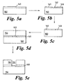
- Figure 5 shows an alternative process flow for the fabrication of a micro-mechanical sensor wherein an insulating layer is provided and an insulating layer 149 is provided on top of a mechanical wafer 150.
- the insulating layer is an oxide which has been grown on to a silicon wafer. This is shown in Figure 5a.
- the insulating layer 149 is patterned and etched using standard techniques so that a portion of the insulating layer is removed creating a void 152.
- the void 152 is refilled using a material which is readily etched by a deep dry etch, or other high aspect ratio etch which will subsequently be used to etch silicon.
- the void was refilled with poly-silicon.
- a second wafer 154 is then bonded, using known techniques, to the insulating layer 149 forming the standard silicon on insulator (SOI) sandwich. As can be seen in Figure 5d the refilled void 152 is sandwiched between the two wafers 150, 154.
- SOI silicon on insulator
- the sandwich is then flipped so that etching can be performed on the mechanical wafer. As discussed earlier it is preferred to etch the wafer on which the insulating layer was grown due to the cleaner interface between the insulating layer 149 and the wafer 150 as opposed to between the wafer 154 to which the insulating layer 149 was bonded.
- the top wafer is ground / polished to the desired thickness and then patterned and etched.
- the etching is again performed by a high aspect ratio process, in this case ASE by STS was used to form the channel 156. It should be noted that as in Figure 5e the channel 156 in the mechanical wafer 150 is aligned with the void 152 created in the insulating layer 149.
- the etch As discussed hereinbefore due to process variations it is difficult to precisely time the etch so that it stops at the boundary between the mechanical wafer 150 and the insulating later 149. If the etch is allowed to over-run then doming of the silicon wafer 150 is likely to occur in regions of the channel 156 neighbouring the insulating layer 149. However, the provision of the filled void 152 over comes this problem. It will be appreciated that the doming occurs due to the preferential etching of silicon compared to the etch rate of the insulating layer 149 and charging at the oxide interface.
- the polysilicon filled void 152 has been arranged to be coincident with the channel 156 so that if the etch overruns it will etch the polysilicon which etches at the same rate as the silicon wafer 150 and is conducting. Thus the doming problem is alleviated.
- Alignment markers passing substantially through the mechanical wafer may be used for this method to ensure that the masks used to etch the mechanical are aligned with the voids 152 created in the insulating layer 149. Indeed, the same mask may be used to etch the mechanical wafer and the insulating layer 149 and the alignment marker may be used to ensure that this mask is correctly orientated before the etch is performed on the mechanical wafer.
- alignment marker may still be possible to align a process on one side of the wafer with a process on the opposite side of the wafer.
- An alignment marker only passing partially through the wafer may be visible using infra red imaging from the side of the wafer on which the alignment marker is not present. Such imaging is commonly available in fabrication plants. Prior art techniques of fabricating alignment markers would not have been visible using infra red imaging.
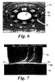
- micro-inertial mechanical sensor which is a ring gyrometer and may be fabricated from silicon.
- a scanning electron micrograph of such a device 101 is shown in Figure 6 and a cross section through line AA of Figure 6 is shown in Figure 7.
- the gyrometer shown in Figure 6 comprises a single ring 99 supported by eight suspensory ligament pairs (a to h) centred at 45° intervals around the ring 99.
- the ring 99 comprises a suspended portion which has been etched from a wafer 102.
- the ligament pairs (a to h) are connected to the ring 99 and connect it to the wafer 102.
- each of the electrode elements forms the plate of a single capacitor, with the ring 99 forming the other plate. That is the plate 99 forms one of the plates of each of eight capacitors, with the other plate being formed by an electrode element.
- the electrode element D 1 is used to drive the ring. A voltage is applied across the capacitor formed by D 1 to cause the ring 99 to oscillate.
- the capacitors formed with the electrode elements P 1,2,3 are used to sense the primary motion of the ring and the capacitors formed with the electrode elements S 1,2,3,4 are used to sense the secondary motion of the ring 99.
- the drive element D 1 can also be used to sense the primary motion of the ring 99.
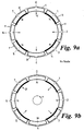
- the primary mode of oscillation of the ring will have four points of zero displacement around the ring 99 (which are marked with N in Figure 9a). The zero points are arranged to occur at where the electrode elements S 1,2,3,4 are situated so that the capacitors formed by these electrode elements only pick up secondary motion. Also, the secondary mode of oscillation of the ring has four points of zero displacement around the ring 99 (marked with N and shown in Figure 9b) and the electrode elements are arranged so the capacitors formed by P 1,2,3 and D 1 only pick up primary motion of the ring 99.
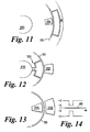
- the electrode elements could also be situated outside the ring 99 possibly within the supporting ligaments as shown at position N in Figure 8.
- the arrangements providing the electrode elements inside and outside the ring are further shown in Figures 11 and 12. It is possible to provide the supporting ligaments 199 to a central region 200. Such an arrangement is shown in Figure 12 in which an electrode element 202 is provided on an outside of the ring 99.
- the arrangement shown in Figure 11 is a schematic representation of a portion of the device shown in Figure 6 with an electrode element 204 inside the ring 99.
- extra electrode elements could be provided which may act as tuning capacitors, in addition to existing drive and sense elements (D,P,S). Such tuning capacitors may be provided at positions intermediate to the electrode elements D 1 , P 1,2,3 , S 1,2,3,4 such as that shown at L in Figure 8.
- the gyrometer has been formed from silicon having an orientation of ⁇ 100 > .
- silicon has anisotropic properties and the modulus of rigidity and the radial Young's modulus varying significantly in a cos4 ⁇ manner through the material. This variation in mechanical properties has important implications for the fabrication of the sensor.
- the gyrometer has also been fabricated from silicon having an orientation of ⁇ 111 > .
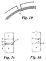
- portions of the ring 99 in the regions of the suspensory ligaments (b, d, f, h) are thickened in comparison to portions of the ring in the region of drive / sense ligaments (a, c, e, g).
- Each of the thickened regions of the ring 99 each extends for a 45° arc around the ring 99 and can be seen in Figures 8 and 9.
- the 45° arcs of thickening are an approximation to a cos4 ⁇ variation. The skilled person will appreciate that an actual cos4 ⁇ variation could be employed.
- the portions of the ring 99 in the regions of suspensory ligaments (b, d, f, h) are thickened relative to the remainder of the ring 99 by an amount h.
- the ring 99 in this example has a base width x of 100 ⁇ m and calculations have shown that the ideal thickening would be 13 ⁇ m i.e. h is 13 ⁇ m. This is most clearly seen in Figure 10. This thickening compensates for the anisotropic properties and allows the gyrometer to function as if were fabricated from ⁇ 111 > silicon which has isotropic properties, or at least more like a ⁇ 111 > silicon sensor.
- x-ray techniques would be used to identify the exact crystal orientation of the wafer which was to be used to fabricate the gyrometer. Once the crystal orientation had been established the exact thickness adjustment required to overcome the misalignment of the crystal could be calculated and appropriate changes made to the mask or trimming techniques could be used to compensate for the misalignment once the gyrometer were fabricated. Such steps would allow the performance of the gyrometer to be tuned precisely to the particular wafer. The skilled person will appreciate it is difficult to cut a silicon crystal with precisely defined crystal orientation and that there will generally always be some error.
- active tuning could be used to compensate for misalignment of the gyrometer relative to the crystal planes.
- An advantage of the use of anisotropically etched alignment markers is that a plurality of wafers may be etched in a single process and the pattern self-aligns to each wafer.
- the gyrometer described herein is fabricated from silicon using processes which are compatible with CMOS processing technology which offers a low cost gyrometer.
- the gyrometer may be provided with on chip processing circuits which may be fabricated within a CMOS facility, or other integrated micro-electronic fabrication facility.
- CMOS processes are typically carried out on ⁇ 100 > orientated silicon wafers, although it is possible to make them on ⁇ 111 > orientated silicon at significant expense.
- Vibratory gyrometers operate by exciting a vibratory primary motion in the structure which experiences a Coriolis force under an applied rate of turn. This force produces a secondary motion the amplitude of which is a measure of the rate of turn. In most devices the primary and secondary motions correspond to two modes of vibration of the structure.
- the electrode elements S 1,2,3,4 are used to measure the secondary motion of the ring 99. It is possible to increase the common mode noise rejection of the gyrometer by using the electrode elements in pairs (perhaps S 1 and S 2 and S 3 and S 4 ). In such an arrangement noise common to both electrode elements in a pair can be eliminated increasing the detected signal. It is also possible to use the arrangement shown in Figure 13 in a differential manner using the electrode element pair 206, 208. It will be appreciated that the arrangement of the pair of electrode elements will be repeated around the ring 99. Use of electrode elements 206,208 in this manner will lead to an increased common mode noise rejection. The arrangement of Figure 13 may provide improved noise rejection compared to the technique of pairing electrode elements of the arrangement of Figure 6.
- Embodiments are described herein wherein a cos4 ⁇ thickness variation occurs around the ring 99.
- This thickness variation may provide an functioning of the gyrometer.
- electrostatic tuning may be used to complete the compensation. Indeed, electrostatic tuning may be applied to improve the performance of a gyrometer without the cos4 ⁇ thickness variation.
- Electrostatic tuning comprises applying a potential to electrode elements in a calculated manner so that electrostatic forces are exerted on the ring 99. These forces can be tailored to compensate for any non-ideal behaviour of the ring 99.
- Such electrostatic tuning may be especially applicable in the embodiment shown in Figure 13 where voltages are applied to the electrode elements 206,208.
- Possible waveforms are shown in Figure 14 which shows ac voltages which are imposed on dc bias voltages.
- the ring 99 is shown along a centre region of Figure 14 and is generally grounded.
- a closed loop arrangement is set up which may improve the functionality of the device.
- a drive electrode element is used to induce a primary oscillation in the ring 99.
- Turning forces induce a secondary harmonic, angled at about 45° to the first harmonic, and it is the amplitude of these oscillations due to the secondary harmonic which can be used to calculate the rate of turn.
- the pair of electrode elements 206,208 as shown in Figure 13, it is possible to detect the secondary harmonic and then apply a voltage to the electrode elements 206,208 such that the secondary harmonic is substantially cancelled (or prevented).
- the rate of turn can then be calculated from the voltage levels which are required to reduce the secondary harmonic to zero.
- Such an arrangement may make the device more linear and/or more stable.
- a gyro structure that may meet these requirements takes the form of a ring 99 that vibrates in the plane of the wafer, shown in Figure 8.
- the desired primary and secondary modes of vibration of the gyrometer are as shown in Figures 9a and 9b, respectively.
- the ring 99 is held in place by eight supporting ligament pairs 100.
- the ring 99 and its ligaments are etched from ⁇ 100 > mechanical silicon wafer.
- a ring fabricated from crystalline silicon will be expected to have predictable material properties, high intrinsic Q, and the thickness required for mechanical stability. These requirements are not reliably obtained with layers deposited on to a silicon wafer.
- ring width 5 ⁇ m-1mm
- width of the supporting ligaments 100 1 ⁇ m to 0.5mm.
- gyrometer a variety of different designs exist other than the one described herein including other transduction techniques. For instance it may be possible to measure the resistance change using the piezo resistive nature of silicon in elements to measure the motion of the ring. It may also be possible to use inductive detectors to measure the motion of the ring perhaps by applying tracking to portions of the ring and applying a magnetic field.
- a silicon crystal is physically and mechanically anisotropic and its radial and tangential elastic stiffness coefficients vary in a cos4 ⁇ manner around the ring.
- the effect of the anisotropy is to cause a split in the frequencies of the drive and sense modes. This split is significant and unless it is compensated for causes a reduction in gyro sensitivity.
- the effects of this anisotropy can be eliminated or substantially reduced by making the width of the ring different (by an amount h as discussed hereinbefore) in those regions associated with the drive and sense ligaments of the drive mode.
- Figure 10 shows the details of the proposed construction and a value of h about 13 ⁇ m is required to match the frequencies for a ring thickness of nominally 100 ⁇ m.
Claims (34)
- Gyromètre en anneau micro-mécanique (101) comprenant un élément en anneau (99) fabriqué d'un matériau ayant des propriétés mécaniques anisotropes caractérisé en ce que l'élément en anneau (99) est agencé pour osciller pendant l'utilisation et en ce qu'au moins une région de l'élément en anneau (99) est épaissie par rapport au reste de l'élément en anneau pour compenser sensiblement lesdites propriétés mécaniques anisotropes du matériau à partir duquel l'élément en anneau (99) est fabriqué.
- Gyromètre selon la revendication 1, dans lequel ladite au moins une région de l'élément en anneau (99) est épaissie par rapport au reste de l'élément en anneau de telle manière que la dimension d'épaisseur de l'élément en anneau varie de manière périodique en fonction du déplacement angulaire autour de l'élément en anneau (99).
- Gyromètre selon la revendication 2, dans lequel la variation périodique se produit autour de l'élément en anneau de manière approximative en cos4θ, où θ est le déplacement angulaire autour de l'élément en anneau (99).
- Gyromètre selon l'une quelconque des revendications précédentes, dans lequel l'élément en anneau (99) est suspendu par un certain nombre de ligaments suspenseurs (a à h) reliant l'élément en anneau (99) à un substrat (102).
- Gyromètre selon la revendication 4, dans lequel les ligaments suspenseurs (a à h) se relient à une surface externe de l'élément en anneau (99).
- Gyromètre selon la revendication 4, dans lequel les ligaments suspenseurs (a à h) se relient à une surface interne de l'élément en anneau (99).
- Gyromètre selon l'une quelconque des revendications 4 à 6, dans lequel les portions épaissies de l'élément en anneau (99) sont grossièrement disposées entre les paires des ligaments suspenseurs (a à h).
- Gyromètre selon l'une quelconque des revendications précédentes, dans lequel l'élément en anneau (99) forme une plaque d'au moins un condensateur, le gyromètre étant agencé de telle sorte que le mouvement de l'élément en anneau (99) amène la valeur du condensateur ainsi formé à varier.
- Gyromètre selon la revendication 8, dans lequel au moins une électrode (D1, P1,2, 3,4, S1,2,3) est formée pour former une seconde plaque du condensateur.
- Gyromètre selon la revendication 9, caractérisé en ce que ladite au moins une électrode (D1, P1, 2, 3, 4, S1, 2,3) comprend une électrode d'entraînement agencée pour entraîner les oscillations de l'élément en anneau (99).
- Gyromètre selon la revendication 10, dans lequel l'électrode d'entraînement est agencée pour entraîner l'élément en anneau (99) dans un premier mode d'oscillation de telle sorte qu'il existe un anti-noeud d'oscillation maximale adjacent à l'électrode d'entraînement.
- Gyromètre selon la revendication 11, dans lequel au moins une électrode de détection de premier mode est formée grossièrement à un entier multiple de 90° autour de l'élément en anneau (99) à partir de ladite au moins une électrode d'entraînement, ladite au moins une électrode de détection de premier mode étant agencée pour détecter l'oscillation du premier mode.
- Gyromètre selon la revendication 12, dans lequel l'élément en anneau est agencé pour avoir un second mode d'oscillation et a au moins une électrode de détection de second mode agencée pour détecter l'oscillation due au second mode d'oscillation.
- Gyromètre selon la revendication 13, dans lequel l'électrode de détection de second mode est agencée à un noeud de déplacement nul du premier mode d'oscillation.
- Gyromètre selon l'une quelconque des revendications précédentes, dans lequel au moins une paire d'électrodes est formée et l'élément en anneau est agencé pour passer entre la paire d'électrodes.
- Gyromètre selon la revendication 15, dans lequel ladite au moins une paire d'électrodes est agencée pour produire des premier et second signaux et le gyromètre est agencé pour traiter différentiellement les premier et second signaux.
- Gyromètre selon l'une quelconque des revendications précédentes, dans lequel il est fabriqué à partir d'un matériau ayant des plans cristallins d'une orientation <100>.
- Procédé de fabrication d'un gyromètre en anneau micro-mécanique (101) comprenant les étapes consistant à :(i) prendre une couche de matériau cristallin (102) ayant des propriétés mécaniques anisotropes ;(ii) déterminer le degré de désalignement du réseau cristallin au sein de ladite couche de matériau (102) en identifiant l'orientation cristalline exacte ;
caractérisé en ce que le procédé comprend en outre les étapes consistant à :(iii) calculer le degré de changement requis dans la dimension d'épaisseur d'un élément en anneau (99) formé dans la couche de matériau cristallin (102) pour compenser le désalignement du réseau cristallin ; et(iv) fabriquer un tel élément en anneau (99) dans ladite couche de matériau (102) dans lequel au moins une région de l'élément en anneau (99) est épaissie par rapport au reste de l'élément en anneau (99) pour compenser sensiblement ledit désalignement et de ce fait les propriétés mécaniques anisotropes de ladite couche de matériau (102). - Procédé selon la revendication 18, dans lequel l'étape (iv) de fabrication d'un élément en anneau (99) comprend les étapes consistant à : prendre une première tranche (2 ; 50) ayant une couche isolante (8, 10, 12, 14 ; 56) formée dessus et ayant une seconde tranche (4 ; 62) liée à la couche isolante (8,10, 12, 14 ; 56) eta) former en motif et attaquer chimiquement ultérieurement l'une de n'importe laquelle des première ou seconde tranches de telle sorte que des canaux (18, 20 ; 52, 54) sont créés dans ladite une tranche (la tranche attaquée chimiquement) se terminant adjacente à la couche isolante (8,10,12,14 ; 56) ; etb) attaquer chimiquement la couche isolante pour éliminer les portions de la couche isolante (8,10, 12,14 ; 56) adjacente à la tranche attaquée chimiquement de telle sorte que ces portions de la tranche attaquée chimiquement en dessous d'une taille prédéterminée, les portions suspendues, deviennent sensiblement librement suspendues au-dessus de l'autre tranche.
- Procédé selon la revendication 19, dans lequel la couche isolante a une épaisseur entre 1,5 µm et 3 µm.
- Procédé selon l'une quelconque des revendications 19 à 20, dans lequel le procédé augmente la masse des portions en dessous de la taille prédéterminée qui sont sensiblement libérées pendant l'étape b) du procédé.
- Procédé selon l'une quelconque des revendications 19 à 21, dans lequel le masque pour l'attaque chimique de l'étape a) est optimisé de sorte que les aires à attaquer chimiquement ont des aires en coupe transversale sensiblement égales.
- Procédé selon l'une quelconque des revendications 19 à 22, dans lequel des ligaments suspenseurs (a à h) sont formés pour joindre les portions suspendues et le reste de la tranche attaquée chimiquement.
- Procédé selon l'une quelconque des revendications 19 à 23, et comprenant en outre les étapes consistant à nettoyer l'attaque chimique de la couche isolante (8, 10, 12, 14 ; 56) avec une vapeur.
- Procédé selon l'une quelconque des revendications 19 à 24, dans lequel certains des canaux (18, 20 ; 52, 54) créés dans la tranche attaquée chimiquement avant d'effectuer l'étape b) sont re-remplis à l'aide d'un matériau de re-remplissage.
- Procédé selon l'une quelconque des revendications 19 à 25, dans lequel des contacts ou pistes d'interconnexion sont enfouis dans la couche isolante au fur et à mesure qu'elle est formée sur la surface de la première tranche (2 ; 50).
- Procédé selon l'une quelconque des revendications 19 à 26, dans lequel la couche isolante (8,10, 12, 14 ; 56) entre les première et seconde tranches comprend plus d'un matériau.
- Procédé selon l'une quelconque des revendications 19 à 27, dans lequel les matériaux formant la couche isolante (8, 10, 12, 14 ; 56) sont des oxydes du matériau à partir duquel la tranche est fabriquée.
- Procédé selon l'une quelconque des revendications 19 à 28, dans lequel une couche de nitrure au sein de la couche isolante reste après l'étape b).
- Procédé selon l'une quelconque des revendications 19 à 29, dans lequel la contrainte entre les première et seconde tranches est réduite en formant la couche isolante (8,10,12,14 ; 56) sous forme de séries de couches.
- Procédé selon l'une quelconque des revendications 19 à 30, dans lequel l'épaisseur de la tranche attaquée chimiquement au début du procédé b) se situe sensiblement dans la gamme de 11 µm à 200 µm.
- Procédé selon la revendication 18, dans lequel l'étape de fabrication d'un élément en anneau (99) comprend les étapes suivantes consistant à :a. former une couche isolante (8, 10, 12, 14 ; 56) sur une surface la plus supérieure d'une première tranche (2 ; 50) ;b. attaquer chimiquement des portions de la couche isolante (8, 10, 12, 14; 56) ;c. lier une seconde tranche (4 ; 62) à la couche isolante (8, 10, 12, 14; 56); etd. attaquer chimiquement une surface la plus inférieure de l'une des tranches, la tranche attaquée chimiquement, dans des régions adjacentes aux portions attaquées chimiquement de la couche isolante (8, 10, 12, 14 ; 56) de telle sorte que les portions de la tranche attaquée chimiquement deviennent sensiblement libres (portions suspendues) du reste des première et seconde tranches.
- Procédé selon la revendication 32, dans lequel la première tranche est attaquée chimiquement pendant l'étape d) du procédé.
- Procédé selon la revendication 32 ou la revendication 33, et comprenant une étape supplémentaire entre les étapes b) et c) dans laquelle les portions de la couche isolante qui ont été attaquées chimiquement sont re-remplies à l'aide d'un matériau de charge.
Priority Applications (1)
| Application Number | Priority Date | Filing Date | Title |
|---|---|---|---|
| EP07004839A EP1808672A3 (fr) | 1998-09-12 | 1999-09-13 | Améliorations concernant le micro-usinage |
Applications Claiming Priority (3)
| Application Number | Priority Date | Filing Date | Title |
|---|---|---|---|
| GBGB9819821.1A GB9819821D0 (en) | 1998-09-12 | 1998-09-12 | Improvements relating to micro-machining |
| GB9819821 | 1998-09-12 | ||
| PCT/GB1999/003028 WO2000016041A2 (fr) | 1998-09-12 | 1999-09-13 | Formation de barreaux suspendus au moyen de substrats soi et application a la fabrication d'un gyrometre vibrant |
Related Child Applications (1)
| Application Number | Title | Priority Date | Filing Date |
|---|---|---|---|
| EP07004839A Division EP1808672A3 (fr) | 1998-09-12 | 1999-09-13 | Améliorations concernant le micro-usinage |
Publications (2)
| Publication Number | Publication Date |
|---|---|
| EP1116008A2 EP1116008A2 (fr) | 2001-07-18 |
| EP1116008B1 true EP1116008B1 (fr) | 2007-07-18 |
Family
ID=10838709
Family Applications (2)
| Application Number | Title | Priority Date | Filing Date |
|---|---|---|---|
| EP07004839A Withdrawn EP1808672A3 (fr) | 1998-09-12 | 1999-09-13 | Améliorations concernant le micro-usinage |
| EP99946323A Expired - Lifetime EP1116008B1 (fr) | 1998-09-12 | 1999-09-13 | Gyrometre vibrant et son procede de fabrication |
Family Applications Before (1)
| Application Number | Title | Priority Date | Filing Date |
|---|---|---|---|
| EP07004839A Withdrawn EP1808672A3 (fr) | 1998-09-12 | 1999-09-13 | Améliorations concernant le micro-usinage |
Country Status (11)
| Country | Link |
|---|---|
| US (2) | US6276205B1 (fr) |
| EP (2) | EP1808672A3 (fr) |
| JP (1) | JP4999227B2 (fr) |
| KR (1) | KR100651769B1 (fr) |
| AT (1) | ATE367570T1 (fr) |
| AU (1) | AU5874099A (fr) |
| CA (1) | CA2343446A1 (fr) |
| DE (1) | DE69936590T2 (fr) |
| GB (1) | GB9819821D0 (fr) |
| NO (1) | NO20011230L (fr) |
| WO (1) | WO2000016041A2 (fr) |
Families Citing this family (67)
| Publication number | Priority date | Publication date | Assignee | Title |
|---|---|---|---|---|
| SE514042C2 (sv) * | 1998-05-08 | 2000-12-18 | Nordic Sensor Technologies Ab | Sensoranordning |
| AT409429B (de) * | 1999-07-15 | 2002-08-26 | Sez Semiconduct Equip Zubehoer | Verfahren zum ätzbehandeln von halbleitersubstraten zwecks freilegen einer metallschicht |
| US6803755B2 (en) | 1999-09-21 | 2004-10-12 | Rockwell Automation Technologies, Inc. | Microelectromechanical system (MEMS) with improved beam suspension |
| US6798312B1 (en) | 1999-09-21 | 2004-09-28 | Rockwell Automation Technologies, Inc. | Microelectromechanical system (MEMS) analog electrical isolator |
| WO2001025798A2 (fr) * | 1999-10-05 | 2001-04-12 | L-3 Communications Corporation | Procede ameliorant les performances de dispositifs micro-usines |
| US6456939B1 (en) * | 2000-01-04 | 2002-09-24 | Mccall Hiram | Micro inertial measurement unit |
| US6525352B1 (en) * | 2000-11-22 | 2003-02-25 | Network Photonics, Inc. | Method to reduce release time of micromachined devices |
| US6815243B2 (en) * | 2001-04-26 | 2004-11-09 | Rockwell Automation Technologies, Inc. | Method of fabricating a microelectromechanical system (MEMS) device using a pre-patterned substrate |
| US6761829B2 (en) | 2001-04-26 | 2004-07-13 | Rockwell Automation Technologies, Inc. | Method for fabricating an isolated microelectromechanical system (MEMS) device using an internal void |
| US6794271B2 (en) * | 2001-09-28 | 2004-09-21 | Rockwell Automation Technologies, Inc. | Method for fabricating a microelectromechanical system (MEMS) device using a pre-patterned bridge |
| US6756310B2 (en) * | 2001-09-26 | 2004-06-29 | Rockwell Automation Technologies, Inc. | Method for constructing an isolate microelectromechanical system (MEMS) device using surface fabrication techniques |
| KR100421217B1 (ko) * | 2001-05-30 | 2004-03-02 | 삼성전자주식회사 | 점착 방지 미세 구조물 제조 방법 |
| US6664786B2 (en) | 2001-07-30 | 2003-12-16 | Rockwell Automation Technologies, Inc. | Magnetic field sensor using microelectromechanical system |
| US6690178B2 (en) | 2001-10-26 | 2004-02-10 | Rockwell Automation Technologies, Inc. | On-board microelectromechanical system (MEMS) sensing device for power semiconductors |
| US6562642B1 (en) * | 2002-02-07 | 2003-05-13 | International Business Machines Corporation | Micro-structures and methods for their manufacture |
| GB0206509D0 (en) | 2002-03-20 | 2002-05-01 | Qinetiq Ltd | Micro-Electromechanical systems |
| GB0206510D0 (en) * | 2002-03-20 | 2002-05-01 | Qinetiq Ltd | Micro-Electromechanical systems |
| EP2386826B1 (fr) * | 2002-06-10 | 2014-02-26 | Panasonic Corporation | Capteur de vitesse angulaire |
| FR2845200A1 (fr) * | 2002-09-26 | 2004-04-02 | Memscap | Procede de fabrication d'un composant electronique incluant une structure micro-electromecanique |
| KR100512988B1 (ko) * | 2002-09-26 | 2005-09-07 | 삼성전자주식회사 | 플렉서블 mems 트랜스듀서 제조방법 |
| US6979408B2 (en) * | 2002-12-30 | 2005-12-27 | Intel Corporation | Method and apparatus for photomask fabrication |
| US6975193B2 (en) * | 2003-03-25 | 2005-12-13 | Rockwell Automation Technologies, Inc. | Microelectromechanical isolating circuit |
| DE10331714B4 (de) * | 2003-07-11 | 2006-05-24 | Micronas Gmbh | Verfahren zur Strukturierung der Oberfläche eines Substrats |
| US20050062362A1 (en) * | 2003-08-28 | 2005-03-24 | Hongyuan Yang | Oscillatory gyroscope |
| US20050076866A1 (en) * | 2003-10-14 | 2005-04-14 | Hopper Mark L. | Electromechanical valve actuator |
| KR100605497B1 (ko) * | 2003-11-27 | 2006-07-28 | 삼성전자주식회사 | 에스오아이 기판들을 제조하는 방법들, 이를 사용하여반도체 소자들을 제조하는 방법들 및 그에 의해 제조된반도체 소자들 |
| TWI245902B (en) * | 2004-05-14 | 2005-12-21 | Chung Shan Inst Of Science | Microstructure angular velocity sensor device |
| CN1985149B (zh) | 2004-07-12 | 2010-11-03 | 住友精密工业株式会社 | 角速度传感器 |
| US20100117152A1 (en) * | 2007-06-28 | 2010-05-13 | Chang-Woo Oh | Semiconductor devices |
| KR100843717B1 (ko) * | 2007-06-28 | 2008-07-04 | 삼성전자주식회사 | 플로팅 바디 소자 및 벌크 바디 소자를 갖는 반도체소자 및그 제조방법 |
| KR100555569B1 (ko) | 2004-08-06 | 2006-03-03 | 삼성전자주식회사 | 절연막에 의해 제한된 채널영역을 갖는 반도체 소자 및 그제조방법 |
| KR100658202B1 (ko) | 2005-09-12 | 2006-12-15 | (주)마이크로인피니티 | 마이크로 구조물의 부양체 및 그 제조방법 |
| US7462509B2 (en) * | 2006-05-16 | 2008-12-09 | International Business Machines Corporation | Dual-sided chip attached modules |
| TWI305930B (en) * | 2006-06-19 | 2009-02-01 | Touch Micro System Tech | Method of fabricating suspended structure |
| US20080108224A1 (en) * | 2006-10-12 | 2008-05-08 | Zhaoning Yu | Patterning methods |
| US20100038825A1 (en) * | 2006-12-21 | 2010-02-18 | Mcdonald Joel P | Methods of forming microchannels by ultrafast pulsed laser direct-write processing |
| IL181367A (en) * | 2007-02-15 | 2013-03-24 | Elbit Systems Electro Optics Elop Ltd | Vibrating gyroscopic device for measuring angular velocity |
| US8056413B2 (en) * | 2007-09-11 | 2011-11-15 | Evigia Systems, Inc. | Sensor and sensing method utilizing symmetrical differential readout |
| ATE520960T1 (de) * | 2007-09-18 | 2011-09-15 | Atlantic Inertial Systems Ltd | Verbesserungen in bezug auf winkelgeschwindigkeitssensoren |
| EP2040032A1 (fr) * | 2007-09-19 | 2009-03-25 | Atlantic Inertial Systems Limited | Améliorations de ou associées aux capteurs de vitesse angulaire |
| US7992438B2 (en) * | 2007-11-28 | 2011-08-09 | Chung Shan Institute Of Science And Technology, Armaments Bureau, M.N.D. | Multiaxial gyroscope |
| US7908922B2 (en) * | 2008-01-24 | 2011-03-22 | Delphi Technologies, Inc. | Silicon integrated angular rate sensor |
| WO2009109969A2 (fr) * | 2008-03-03 | 2009-09-11 | Ramot At Tel-Aviv University Ltd. | Capteurs de vitesse mécaniques à micro-échelle |
| US8451077B2 (en) | 2008-04-22 | 2013-05-28 | International Business Machines Corporation | MEMS switches with reduced switching voltage and methods of manufacture |
| GB0812788D0 (en) * | 2008-07-12 | 2008-08-20 | Atlantic Inertial Systems Ltd | Improvements in or relating to vibrating structure gyroscopes |
| US8263426B2 (en) | 2008-12-03 | 2012-09-11 | Electronics And Telecommunications Research Institute | High-sensitivity z-axis vibration sensor and method of fabricating the same |
| JP2012528335A (ja) * | 2009-05-27 | 2012-11-12 | キング アブドゥーラ ユニバーシティ オブ サイエンス アンド テクノロジー | 面外サスペンション方式を使用するmems質量−バネ−ダンパシステム |
| CN102472648B (zh) * | 2009-07-22 | 2014-04-16 | 皇家飞利浦电子股份有限公司 | 具有低响应时间和高灵敏度的热流量传感器集成电路 |
| US20120244969A1 (en) | 2011-03-25 | 2012-09-27 | May Patents Ltd. | System and Method for a Motion Sensing Device |
| JP5708222B2 (ja) * | 2011-05-12 | 2015-04-30 | 大日本印刷株式会社 | 力学量センサー |
| TWI456201B (zh) * | 2011-11-29 | 2014-10-11 | Univ Chung Hua | 無線式熱氣泡式加速儀及其製備方法 |
| US20130201316A1 (en) | 2012-01-09 | 2013-08-08 | May Patents Ltd. | System and method for server based control |
| US9006077B2 (en) * | 2013-08-21 | 2015-04-14 | GlobalFoundries, Inc. | Gate length independent silicon-on-nothing (SON) scheme for bulk FinFETs |
| JP6173851B2 (ja) | 2013-09-20 | 2017-08-02 | 株式会社日立ハイテクノロジーズ | 分析方法およびプラズマエッチング装置 |
| US9661215B2 (en) | 2014-04-22 | 2017-05-23 | Snapaid Ltd. | System and method for controlling a camera based on processing an image captured by other camera |
| EP2952979B1 (fr) * | 2014-06-03 | 2017-03-01 | Nivarox-FAR S.A. | Composant horloger à base de verre photostructurable |
| EP3289430B1 (fr) | 2015-04-27 | 2019-10-23 | Snap-Aid Patents Ltd. | Estimation et utilisation de posture de tête relative et champ de vision de caméra |
| DE102015118346A1 (de) * | 2015-10-27 | 2017-04-27 | Endress+Hauser Flowtec Ag | MEMS Sensor zu Messung mindestens einer Messgröße |
| US11190374B2 (en) | 2017-08-28 | 2021-11-30 | Bright Data Ltd. | System and method for improving content fetching by selecting tunnel devices |
| EP4187881A1 (fr) | 2017-08-28 | 2023-05-31 | Bright Data Ltd. | Amélioration de l'extraction de contenu par sélection de dispositifs tunnel groupés en fonction d'un emplacement géographique |
| EP3652721A1 (fr) | 2017-09-04 | 2020-05-20 | NNG Software Developing and Commercial LLC | Procédé et appareil de collecte et d'utilisation de données de capteur provenant d'un véhicule |
| KR102086230B1 (ko) * | 2018-06-26 | 2020-03-06 | 한국과학기술원 | 굴절률 및 스트레인의 주기적 동시변화를 이용한 공진기와 전하구속 구조 일체형 주기성 다리 구조 및 그 제조 방법 |
| EP3888346A4 (fr) | 2019-02-19 | 2022-08-24 | Edgy Bees Ltd. | Estimation d'un retard en temps réel d'un flux de données vidéo |
| LT3780557T (lt) | 2019-02-25 | 2023-03-10 | Bright Data Ltd. | Turinio parsisiuntimo, naudojant url bandymų mechanizmą, sistema ir būdas |
| EP3935792A4 (fr) | 2019-04-02 | 2022-11-30 | Bright Data Ltd. | Système et procédé de gestion d'un service d'extraction non directe d'url |
| CN109974681B (zh) * | 2019-04-09 | 2021-01-26 | 东南大学 | 一种基于光波导的盘式谐振陀螺仪及其加工封装方法 |
| WO2024042819A1 (fr) * | 2022-08-25 | 2024-02-29 | 住友精密工業株式会社 | Détecteur de vitesse angulaire de type à vibration |
Family Cites Families (26)
| Publication number | Priority date | Publication date | Assignee | Title |
|---|---|---|---|---|
| JPS63202035A (ja) * | 1987-02-17 | 1988-08-22 | Mitsubishi Electric Corp | 半導体装置の製造方法 |
| US4968628A (en) | 1988-12-09 | 1990-11-06 | Harris Corporation | Method of fabricating back diffused bonded oxide substrates |
| US5238223A (en) * | 1989-08-11 | 1993-08-24 | Robert Bosch Gmbh | Method of making a microvalve |
| DE69218611T2 (de) * | 1991-06-12 | 1997-07-03 | Harris Corp | Verfahren zur herstellung eines halbleiter-beschleunigungsmessers |
| DE69232432T2 (de) | 1991-11-20 | 2002-07-18 | Canon Kk | Verfahren zur Herstellung einer Halbleiteranordnung |
| DE4309917A1 (de) | 1992-03-30 | 1993-10-07 | Awa Microelectronics | Verfahren zur Herstellung von Siliziummikrostrukturen sowie Siliziummikrostruktur |
| JP3367113B2 (ja) | 1992-04-27 | 2003-01-14 | 株式会社デンソー | 加速度センサ |
| CA2154357C (fr) | 1993-02-04 | 2004-03-02 | Kevin A. Shaw | Microstructures et methode a un seul masque et a cristal unique pour leur obtention |
| GB2276976B (en) | 1993-04-07 | 1996-10-23 | British Aerospace | Method of manufacturing a motion sensor |
| DE4315012B4 (de) | 1993-05-06 | 2007-01-11 | Robert Bosch Gmbh | Verfahren zur Herstellung von Sensoren und Sensor |
| US5324683A (en) | 1993-06-02 | 1994-06-28 | Motorola, Inc. | Method of forming a semiconductor structure having an air region |
| DE4332057A1 (de) | 1993-09-21 | 1995-03-30 | Siemens Ag | Integrierte mikromechanische Sensorvorrichtung und Verfahren zu deren Herstellung |
| US5415726A (en) | 1993-12-21 | 1995-05-16 | Delco Electronics Corporation | Method of making a bridge-supported accelerometer structure |
| US5511428A (en) | 1994-06-10 | 1996-04-30 | Massachusetts Institute Of Technology | Backside contact of sensor microstructures |
| US5495760A (en) * | 1994-07-05 | 1996-03-05 | Rockwell International Corporation | Beermug gyroscope |
| GB2292609B (en) | 1994-08-24 | 1998-04-15 | British Aerospace | Method for matching vibration mode frequencies on a vibrating structure |
| AU2683995A (en) | 1994-09-02 | 1996-03-27 | Stichting Voor De Technische Wetenschappen | Process for producing micromechanical structures by means of reactive ion etching |
| GB2299669B (en) * | 1995-04-07 | 1998-12-16 | British Aerospace | Method for actively balancing a vibrating structure gyroscope sensing element structure |
| JPH0914570A (ja) | 1995-06-27 | 1997-01-17 | Tokyo Gas Co Ltd | ライフライン管路の耐震強化装置 |
| JPH09145740A (ja) | 1995-09-22 | 1997-06-06 | Denso Corp | 加速度センサ |
| DE19537814B4 (de) | 1995-10-11 | 2009-11-19 | Robert Bosch Gmbh | Sensor und Verfahren zur Herstellung eines Sensors |
| US5721162A (en) | 1995-11-03 | 1998-02-24 | Delco Electronics Corporation | All-silicon monolithic motion sensor with integrated conditioning circuit |
| WO1997022140A2 (fr) | 1995-11-29 | 1997-06-19 | Litton Systems, Inc. | Procede permettant de purger un substrat sacrificiel multicouche au silicium soumis a une attaque acide |
| US6048774A (en) * | 1997-06-26 | 2000-04-11 | Denso Corporation | Method of manufacturing dynamic amount semiconductor sensor |
| US6075639A (en) * | 1997-10-22 | 2000-06-13 | The Board Of Trustees Of The Leland Stanford Junior University | Micromachined scanning torsion mirror and method |
| US6159385A (en) * | 1998-05-08 | 2000-12-12 | Rockwell Technologies, Llc | Process for manufacture of micro electromechanical devices having high electrical isolation |
-
1998
- 1998-09-12 GB GBGB9819821.1A patent/GB9819821D0/en not_active Ceased
- 1998-09-30 US US09/163,554 patent/US6276205B1/en not_active Expired - Lifetime
-
1999
- 1999-09-13 WO PCT/GB1999/003028 patent/WO2000016041A2/fr active IP Right Grant
- 1999-09-13 AU AU58740/99A patent/AU5874099A/en not_active Abandoned
- 1999-09-13 CA CA002343446A patent/CA2343446A1/fr not_active Abandoned
- 1999-09-13 KR KR1020017003168A patent/KR100651769B1/ko not_active IP Right Cessation
- 1999-09-13 DE DE69936590T patent/DE69936590T2/de not_active Expired - Lifetime
- 1999-09-13 JP JP2000570531A patent/JP4999227B2/ja not_active Expired - Fee Related
- 1999-09-13 EP EP07004839A patent/EP1808672A3/fr not_active Withdrawn
- 1999-09-13 EP EP99946323A patent/EP1116008B1/fr not_active Expired - Lifetime
- 1999-09-13 AT AT99946323T patent/ATE367570T1/de not_active IP Right Cessation
-
2001
- 2001-03-09 NO NO20011230A patent/NO20011230L/no not_active Application Discontinuation
- 2001-07-05 US US09/898,081 patent/US6670212B2/en not_active Expired - Fee Related
Also Published As
| Publication number | Publication date |
|---|---|
| WO2000016041A3 (fr) | 2000-09-28 |
| US20020017132A1 (en) | 2002-02-14 |
| JP2002525843A (ja) | 2002-08-13 |
| CA2343446A1 (fr) | 2000-03-23 |
| NO20011230L (no) | 2001-05-11 |
| WO2000016041A2 (fr) | 2000-03-23 |
| JP4999227B2 (ja) | 2012-08-15 |
| US6276205B1 (en) | 2001-08-21 |
| EP1808672A2 (fr) | 2007-07-18 |
| AU5874099A (en) | 2000-04-03 |
| KR100651769B1 (ko) | 2006-11-30 |
| DE69936590T2 (de) | 2007-11-22 |
| GB9819821D0 (en) | 1998-11-04 |
| EP1116008A2 (fr) | 2001-07-18 |
| KR20010075052A (ko) | 2001-08-09 |
| ATE367570T1 (de) | 2007-08-15 |
| NO20011230D0 (no) | 2001-03-09 |
| US6670212B2 (en) | 2003-12-30 |
| EP1808672A3 (fr) | 2009-06-17 |
| DE69936590D1 (de) | 2007-08-30 |
Similar Documents
| Publication | Publication Date | Title |
|---|---|---|
| EP1116008B1 (fr) | Gyrometre vibrant et son procede de fabrication | |
| EP2083246B1 (fr) | Capteur de débit angulaire intégré en silicone | |
| Ayazi et al. | High aspect-ratio combined poly and single-crystal silicon (HARPSS) MEMS technology | |
| US7645627B2 (en) | Method for manufacturing a sensor device | |
| US6988408B2 (en) | Surface/bulk micromachined single-crystalline silicon micro-gyroscope | |
| US5535902A (en) | Gimballed vibrating wheel gyroscope | |
| EP0400939B1 (fr) | Capteur semi-conducteur à élément vibrant | |
| US7312553B2 (en) | Micromechanical component and method for producing same | |
| JP3037416B2 (ja) | マイクロメカニック式の回転値センサ | |
| Cho et al. | A high-Q birdbath resonator gyroscope (BRG) | |
| US11277112B2 (en) | Micro-electro-mechanical device with reduced temperature sensitivity and manufacturing method thereof | |
| EP3335004B1 (fr) | Capteurs de vitesse angulaire | |
| US8443665B2 (en) | Frequency modulated micro gyro | |
| US6242276B1 (en) | Method for fabricating micro inertia sensor | |
| JP4362877B2 (ja) | 角速度センサ | |
| Ayazi et al. | High aspect-ratio dry-release poly-silicon MEMS technology for inertial-grade microgyroscopes | |
| US20020017133A1 (en) | Surface/bulk micromachined single-crystalline silicon micro-gyroscope | |
| JP2004004119A (ja) | 半導体力学量センサ | |
| JP4362739B2 (ja) | 振動型角速度センサ | |
| JP2002148278A (ja) | 半導体力学量センサとその製造方法 | |
| KR100233848B1 (ko) | 마이크로 자이로스코프 제조 방법 | |
| Piot et al. | Electromechanical and process design of a 3 axis piezoelectric MEMS gyro in GaAs |
Legal Events
| Date | Code | Title | Description |
|---|---|---|---|
| PUAI | Public reference made under article 153(3) epc to a published international application that has entered the european phase |
Free format text: ORIGINAL CODE: 0009012 |
|
| 17P | Request for examination filed |
Effective date: 20010310 |
|
| AK | Designated contracting states |
Kind code of ref document: A2 Designated state(s): AT BE CH CY DE DK ES FI FR GB GR IE IT LI LU MC NL PT SE |
|
| AX | Request for extension of the european patent |
Free format text: AL;LT;LV;MK;RO;SI |
|
| RAP1 | Party data changed (applicant data changed or rights of an application transferred) |
Owner name: QINETIQ LIMITED |
|
| 17Q | First examination report despatched |
Effective date: 20040809 |
|
| GRAP | Despatch of communication of intention to grant a patent |
Free format text: ORIGINAL CODE: EPIDOSNIGR1 |
|
| RTI1 | Title (correction) |
Free format text: VIBRATING GYROMETER AND ITS PROCESS OF FABRICATION |
|
| GRAS | Grant fee paid |
Free format text: ORIGINAL CODE: EPIDOSNIGR3 |
|
| GRAA | (expected) grant |
Free format text: ORIGINAL CODE: 0009210 |
|
| AK | Designated contracting states |
Kind code of ref document: B1 Designated state(s): AT BE CH CY DE DK ES FI FR GB GR IE IT LI LU MC NL PT SE |
|
| REG | Reference to a national code |
Ref country code: GB Ref legal event code: FG4D |
|
| REG | Reference to a national code |
Ref country code: CH Ref legal event code: EP |
|
| REF | Corresponds to: |
Ref document number: 69936590 Country of ref document: DE Date of ref document: 20070830 Kind code of ref document: P |
|
| REG | Reference to a national code |
Ref country code: CH Ref legal event code: NV Representative=s name: E. BLUM & CO. AG PATENT- UND MARKENANWAELTE VSP |
|
| REG | Reference to a national code |
Ref country code: IE Ref legal event code: FG4D |
|
| ET | Fr: translation filed | ||
| PG25 | Lapsed in a contracting state [announced via postgrant information from national office to epo] |
Ref country code: PT Free format text: LAPSE BECAUSE OF FAILURE TO SUBMIT A TRANSLATION OF THE DESCRIPTION OR TO PAY THE FEE WITHIN THE PRESCRIBED TIME-LIMIT Effective date: 20071218 Ref country code: NL Free format text: LAPSE BECAUSE OF FAILURE TO SUBMIT A TRANSLATION OF THE DESCRIPTION OR TO PAY THE FEE WITHIN THE PRESCRIBED TIME-LIMIT Effective date: 20070718 Ref country code: ES Free format text: LAPSE BECAUSE OF FAILURE TO SUBMIT A TRANSLATION OF THE DESCRIPTION OR TO PAY THE FEE WITHIN THE PRESCRIBED TIME-LIMIT Effective date: 20071029 |
|
| NLV1 | Nl: lapsed or annulled due to failure to fulfill the requirements of art. 29p and 29m of the patents act | ||
| PG25 | Lapsed in a contracting state [announced via postgrant information from national office to epo] |
Ref country code: AT Free format text: LAPSE BECAUSE OF FAILURE TO SUBMIT A TRANSLATION OF THE DESCRIPTION OR TO PAY THE FEE WITHIN THE PRESCRIBED TIME-LIMIT Effective date: 20070718 |
|
| PG25 | Lapsed in a contracting state [announced via postgrant information from national office to epo] |
Ref country code: BE Free format text: LAPSE BECAUSE OF FAILURE TO SUBMIT A TRANSLATION OF THE DESCRIPTION OR TO PAY THE FEE WITHIN THE PRESCRIBED TIME-LIMIT Effective date: 20070718 |
|
| PG25 | Lapsed in a contracting state [announced via postgrant information from national office to epo] |
Ref country code: MC Free format text: LAPSE BECAUSE OF NON-PAYMENT OF DUE FEES Effective date: 20070930 Ref country code: GR Free format text: LAPSE BECAUSE OF FAILURE TO SUBMIT A TRANSLATION OF THE DESCRIPTION OR TO PAY THE FEE WITHIN THE PRESCRIBED TIME-LIMIT Effective date: 20071019 Ref country code: DK Free format text: LAPSE BECAUSE OF FAILURE TO SUBMIT A TRANSLATION OF THE DESCRIPTION OR TO PAY THE FEE WITHIN THE PRESCRIBED TIME-LIMIT Effective date: 20070718 |
|
| PLBE | No opposition filed within time limit |
Free format text: ORIGINAL CODE: 0009261 |
|
| STAA | Information on the status of an ep patent application or granted ep patent |
Free format text: STATUS: NO OPPOSITION FILED WITHIN TIME LIMIT |
|
| 26N | No opposition filed |
Effective date: 20080421 |
|
| PG25 | Lapsed in a contracting state [announced via postgrant information from national office to epo] |
Ref country code: SE Free format text: LAPSE BECAUSE OF FAILURE TO SUBMIT A TRANSLATION OF THE DESCRIPTION OR TO PAY THE FEE WITHIN THE PRESCRIBED TIME-LIMIT Effective date: 20071018 |
|
| PG25 | Lapsed in a contracting state [announced via postgrant information from national office to epo] |
Ref country code: IE Free format text: LAPSE BECAUSE OF NON-PAYMENT OF DUE FEES Effective date: 20070913 |
|
| PG25 | Lapsed in a contracting state [announced via postgrant information from national office to epo] |
Ref country code: CY Free format text: LAPSE BECAUSE OF FAILURE TO SUBMIT A TRANSLATION OF THE DESCRIPTION OR TO PAY THE FEE WITHIN THE PRESCRIBED TIME-LIMIT Effective date: 20070718 |
|
| PG25 | Lapsed in a contracting state [announced via postgrant information from national office to epo] |
Ref country code: LU Free format text: LAPSE BECAUSE OF NON-PAYMENT OF DUE FEES Effective date: 20070913 |
|
| PGFP | Annual fee paid to national office [announced via postgrant information from national office to epo] |
Ref country code: FI Payment date: 20090915 Year of fee payment: 11 Ref country code: CH Payment date: 20090923 Year of fee payment: 11 |
|
| PG25 | Lapsed in a contracting state [announced via postgrant information from national office to epo] |
Ref country code: IT Free format text: LAPSE BECAUSE OF NON-PAYMENT OF DUE FEES Effective date: 20070930 |
|
| REG | Reference to a national code |
Ref country code: CH Ref legal event code: PL |
|
| PG25 | Lapsed in a contracting state [announced via postgrant information from national office to epo] |
Ref country code: FI Free format text: LAPSE BECAUSE OF NON-PAYMENT OF DUE FEES Effective date: 20100913 |
|
| PG25 | Lapsed in a contracting state [announced via postgrant information from national office to epo] |
Ref country code: LI Free format text: LAPSE BECAUSE OF NON-PAYMENT OF DUE FEES Effective date: 20100930 Ref country code: CH Free format text: LAPSE BECAUSE OF NON-PAYMENT OF DUE FEES Effective date: 20100930 |
|
| PGFP | Annual fee paid to national office [announced via postgrant information from national office to epo] |
Ref country code: GB Payment date: 20120920 Year of fee payment: 14 |
|
| PGFP | Annual fee paid to national office [announced via postgrant information from national office to epo] |
Ref country code: DE Payment date: 20120921 Year of fee payment: 14 |
|
| PGFP | Annual fee paid to national office [announced via postgrant information from national office to epo] |
Ref country code: FR Payment date: 20121010 Year of fee payment: 14 |
|
| GBPC | Gb: european patent ceased through non-payment of renewal fee |
Effective date: 20130913 |
|
| REG | Reference to a national code |
Ref country code: DE Ref legal event code: R119 Ref document number: 69936590 Country of ref document: DE Effective date: 20140401 |
|
| REG | Reference to a national code |
Ref country code: FR Ref legal event code: ST Effective date: 20140530 |
|
| PG25 | Lapsed in a contracting state [announced via postgrant information from national office to epo] |
Ref country code: GB Free format text: LAPSE BECAUSE OF NON-PAYMENT OF DUE FEES Effective date: 20130913 |
|
| PG25 | Lapsed in a contracting state [announced via postgrant information from national office to epo] |
Ref country code: FR Free format text: LAPSE BECAUSE OF NON-PAYMENT OF DUE FEES Effective date: 20130930 Ref country code: DE Free format text: LAPSE BECAUSE OF NON-PAYMENT OF DUE FEES Effective date: 20140401 |