EP1116008B1 - Vibrationskreisels und sein herstellungsverfahren - Google Patents
Vibrationskreisels und sein herstellungsverfahren Download PDFInfo
- Publication number
- EP1116008B1 EP1116008B1 EP99946323A EP99946323A EP1116008B1 EP 1116008 B1 EP1116008 B1 EP 1116008B1 EP 99946323 A EP99946323 A EP 99946323A EP 99946323 A EP99946323 A EP 99946323A EP 1116008 B1 EP1116008 B1 EP 1116008B1
- Authority
- EP
- European Patent Office
- Prior art keywords
- wafer
- insulating layer
- ring element
- gyrometer
- portions
- Prior art date
- Legal status (The legal status is an assumption and is not a legal conclusion. Google has not performed a legal analysis and makes no representation as to the accuracy of the status listed.)
- Expired - Lifetime
Links
- 238000000034 method Methods 0.000 title claims abstract description 166
- 238000004519 manufacturing process Methods 0.000 title claims abstract description 21
- 230000008569 process Effects 0.000 title claims description 64
- 238000005530 etching Methods 0.000 claims abstract description 44
- 238000000059 patterning Methods 0.000 claims abstract description 4
- 235000012431 wafers Nutrition 0.000 claims description 285
- 239000000463 material Substances 0.000 claims description 85
- 210000003041 ligament Anatomy 0.000 claims description 28
- 239000013078 crystal Substances 0.000 claims description 26
- 150000004767 nitrides Chemical class 0.000 claims description 23
- 230000010355 oscillation Effects 0.000 claims description 16
- 230000033001 locomotion Effects 0.000 claims description 15
- 239000003990 capacitor Substances 0.000 claims description 14
- 239000000945 filler Substances 0.000 claims description 8
- 238000006073 displacement reaction Methods 0.000 claims description 7
- 238000004140 cleaning Methods 0.000 claims description 5
- 230000008859 change Effects 0.000 claims description 4
- 239000002178 crystalline material Substances 0.000 claims description 4
- 239000000758 substrate Substances 0.000 claims description 4
- 230000000737 periodic effect Effects 0.000 claims description 3
- 239000010703 silicon Substances 0.000 abstract description 81
- 229910052710 silicon Inorganic materials 0.000 abstract description 80
- 238000005516 engineering process Methods 0.000 abstract description 8
- 239000012212 insulator Substances 0.000 abstract description 8
- 239000010410 layer Substances 0.000 description 252
- XUIMIQQOPSSXEZ-UHFFFAOYSA-N Silicon Chemical compound [Si] XUIMIQQOPSSXEZ-UHFFFAOYSA-N 0.000 description 78
- 230000008901 benefit Effects 0.000 description 22
- 238000005334 plasma enhanced chemical vapour deposition Methods 0.000 description 19
- 238000000623 plasma-assisted chemical vapour deposition Methods 0.000 description 19
- 238000012545 processing Methods 0.000 description 19
- 230000001965 increasing effect Effects 0.000 description 18
- 239000003550 marker Substances 0.000 description 13
- 230000000694 effects Effects 0.000 description 10
- 238000005498 polishing Methods 0.000 description 10
- 239000003795 chemical substances by application Substances 0.000 description 9
- 229910021420 polycrystalline silicon Inorganic materials 0.000 description 8
- 239000011800 void material Substances 0.000 description 8
- 239000002019 doping agent Substances 0.000 description 7
- 238000001312 dry etching Methods 0.000 description 7
- 229920005591 polysilicon Polymers 0.000 description 7
- 239000000126 substance Substances 0.000 description 7
- VYPSYNLAJGMNEJ-UHFFFAOYSA-N Silicium dioxide Chemical compound O=[Si]=O VYPSYNLAJGMNEJ-UHFFFAOYSA-N 0.000 description 6
- 238000002120 advanced silicon etching Methods 0.000 description 6
- 230000035945 sensitivity Effects 0.000 description 6
- 230000008719 thickening Effects 0.000 description 6
- 239000004642 Polyimide Substances 0.000 description 5
- 238000013461 design Methods 0.000 description 5
- 239000007788 liquid Substances 0.000 description 5
- 230000000873 masking effect Effects 0.000 description 5
- 238000005459 micromachining Methods 0.000 description 5
- 229920001721 polyimide Polymers 0.000 description 5
- 230000009286 beneficial effect Effects 0.000 description 4
- 239000004020 conductor Substances 0.000 description 4
- 238000000151 deposition Methods 0.000 description 4
- BHEPBYXIRTUNPN-UHFFFAOYSA-N hydridophosphorus(.) (triplet) Chemical compound [PH] BHEPBYXIRTUNPN-UHFFFAOYSA-N 0.000 description 4
- 239000012071 phase Substances 0.000 description 4
- YCKRFDGAMUMZLT-UHFFFAOYSA-N Fluorine atom Chemical compound [F] YCKRFDGAMUMZLT-UHFFFAOYSA-N 0.000 description 3
- 238000009835 boiling Methods 0.000 description 3
- 229910052731 fluorine Inorganic materials 0.000 description 3
- 239000011737 fluorine Substances 0.000 description 3
- 238000000227 grinding Methods 0.000 description 3
- 150000002500 ions Chemical class 0.000 description 3
- 238000004518 low pressure chemical vapour deposition Methods 0.000 description 3
- 238000001465 metallisation Methods 0.000 description 3
- 229920002120 photoresistant polymer Polymers 0.000 description 3
- 238000001020 plasma etching Methods 0.000 description 3
- 229920000642 polymer Polymers 0.000 description 3
- 230000009467 reduction Effects 0.000 description 3
- 229910021332 silicide Inorganic materials 0.000 description 3
- 229910052814 silicon oxide Inorganic materials 0.000 description 3
- 238000010561 standard procedure Methods 0.000 description 3
- 239000000725 suspension Substances 0.000 description 3
- 239000013077 target material Substances 0.000 description 3
- ZOXJGFHDIHLPTG-UHFFFAOYSA-N Boron Chemical compound [B] ZOXJGFHDIHLPTG-UHFFFAOYSA-N 0.000 description 2
- 229910052581 Si3N4 Inorganic materials 0.000 description 2
- 229910052787 antimony Inorganic materials 0.000 description 2
- WATWJIUSRGPENY-UHFFFAOYSA-N antimony atom Chemical compound [Sb] WATWJIUSRGPENY-UHFFFAOYSA-N 0.000 description 2
- 229910052785 arsenic Inorganic materials 0.000 description 2
- RQNWIZPPADIBDY-UHFFFAOYSA-N arsenic atom Chemical compound [As] RQNWIZPPADIBDY-UHFFFAOYSA-N 0.000 description 2
- 238000010420 art technique Methods 0.000 description 2
- 229910052796 boron Inorganic materials 0.000 description 2
- 230000008878 coupling Effects 0.000 description 2
- 238000010168 coupling process Methods 0.000 description 2
- 238000005859 coupling reaction Methods 0.000 description 2
- 230000001419 dependent effect Effects 0.000 description 2
- 230000008021 deposition Effects 0.000 description 2
- 238000005137 deposition process Methods 0.000 description 2
- 239000003814 drug Substances 0.000 description 2
- 229910052732 germanium Inorganic materials 0.000 description 2
- GNPVGFCGXDBREM-UHFFFAOYSA-N germanium atom Chemical compound [Ge] GNPVGFCGXDBREM-UHFFFAOYSA-N 0.000 description 2
- 238000009616 inductively coupled plasma Methods 0.000 description 2
- 238000003331 infrared imaging Methods 0.000 description 2
- 230000037361 pathway Effects 0.000 description 2
- 238000007517 polishing process Methods 0.000 description 2
- 239000000377 silicon dioxide Substances 0.000 description 2
- 235000012239 silicon dioxide Nutrition 0.000 description 2
- HQVNEWCFYHHQES-UHFFFAOYSA-N silicon nitride Chemical compound N12[Si]34N5[Si]62N3[Si]51N64 HQVNEWCFYHHQES-UHFFFAOYSA-N 0.000 description 2
- 238000009966 trimming Methods 0.000 description 2
- 238000001039 wet etching Methods 0.000 description 2
- BOTDANWDWHJENH-UHFFFAOYSA-N Tetraethyl orthosilicate Chemical compound CCO[Si](OCC)(OCC)OCC BOTDANWDWHJENH-UHFFFAOYSA-N 0.000 description 1
- 230000001133 acceleration Effects 0.000 description 1
- 230000004075 alteration Effects 0.000 description 1
- 238000004873 anchoring Methods 0.000 description 1
- 238000000137 annealing Methods 0.000 description 1
- 230000004888 barrier function Effects 0.000 description 1
- 230000015572 biosynthetic process Effects 0.000 description 1
- 238000003486 chemical etching Methods 0.000 description 1
- 238000005229 chemical vapour deposition Methods 0.000 description 1
- 238000010276 construction Methods 0.000 description 1
- 229910021419 crystalline silicon Inorganic materials 0.000 description 1
- 238000012938 design process Methods 0.000 description 1
- 238000001514 detection method Methods 0.000 description 1
- 229910003460 diamond Inorganic materials 0.000 description 1
- 239000010432 diamond Substances 0.000 description 1
- 238000001035 drying Methods 0.000 description 1
- 230000007613 environmental effect Effects 0.000 description 1
- 238000003384 imaging method Methods 0.000 description 1
- 230000006872 improvement Effects 0.000 description 1
- 238000011065 in-situ storage Methods 0.000 description 1
- 238000010348 incorporation Methods 0.000 description 1
- 230000001939 inductive effect Effects 0.000 description 1
- 230000010354 integration Effects 0.000 description 1
- 238000010884 ion-beam technique Methods 0.000 description 1
- 239000007791 liquid phase Substances 0.000 description 1
- 239000012528 membrane Substances 0.000 description 1
- 238000004377 microelectronic Methods 0.000 description 1
- 238000012856 packing Methods 0.000 description 1
- 230000003071 parasitic effect Effects 0.000 description 1
- 230000004044 response Effects 0.000 description 1
- 238000001878 scanning electron micrograph Methods 0.000 description 1
- 239000004065 semiconductor Substances 0.000 description 1
- FVBUAEGBCNSCDD-UHFFFAOYSA-N silicide(4-) Chemical compound [Si-4] FVBUAEGBCNSCDD-UHFFFAOYSA-N 0.000 description 1
- 239000002210 silicon-based material Substances 0.000 description 1
- 238000004611 spectroscopical analysis Methods 0.000 description 1
- 239000010421 standard material Substances 0.000 description 1
- 239000002344 surface layer Substances 0.000 description 1
- 230000026683 transduction Effects 0.000 description 1
- 238000010361 transduction Methods 0.000 description 1
- 238000007514 turning Methods 0.000 description 1
- XLYOFNOQVPJJNP-UHFFFAOYSA-N water Substances O XLYOFNOQVPJJNP-UHFFFAOYSA-N 0.000 description 1
- 238000009736 wetting Methods 0.000 description 1
Images


Classifications
-
- H—ELECTRICITY
- H01—ELECTRIC ELEMENTS
- H01L—SEMICONDUCTOR DEVICES NOT COVERED BY CLASS H10
- H01L29/00—Semiconductor devices adapted for rectifying, amplifying, oscillating or switching, or capacitors or resistors with at least one potential-jump barrier or surface barrier, e.g. PN junction depletion layer or carrier concentration layer; Details of semiconductor bodies or of electrodes thereof ; Multistep manufacturing processes therefor
- H01L29/66—Types of semiconductor device ; Multistep manufacturing processes therefor
- H01L29/84—Types of semiconductor device ; Multistep manufacturing processes therefor controllable by variation of applied mechanical force, e.g. of pressure
-
- G—PHYSICS
- G01—MEASURING; TESTING
- G01C—MEASURING DISTANCES, LEVELS OR BEARINGS; SURVEYING; NAVIGATION; GYROSCOPIC INSTRUMENTS; PHOTOGRAMMETRY OR VIDEOGRAMMETRY
- G01C19/00—Gyroscopes; Turn-sensitive devices using vibrating masses; Turn-sensitive devices without moving masses; Measuring angular rate using gyroscopic effects
- G01C19/56—Turn-sensitive devices using vibrating masses, e.g. vibratory angular rate sensors based on Coriolis forces
Landscapes
- Engineering & Computer Science (AREA)
- Physics & Mathematics (AREA)
- General Physics & Mathematics (AREA)
- Power Engineering (AREA)
- Microelectronics & Electronic Packaging (AREA)
- Radar, Positioning & Navigation (AREA)
- Remote Sensing (AREA)
- Ceramic Engineering (AREA)
- Condensed Matter Physics & Semiconductors (AREA)
- Computer Hardware Design (AREA)
- Pressure Sensors (AREA)
- Gyroscopes (AREA)
- Micromachines (AREA)
- Press Drives And Press Lines (AREA)
- Electrical Discharge Machining, Electrochemical Machining, And Combined Machining (AREA)
- Physical Vapour Deposition (AREA)
- Piezo-Electric Or Mechanical Vibrators, Or Delay Or Filter Circuits (AREA)
- Producing Shaped Articles From Materials (AREA)
- Oscillators With Electromechanical Resonators (AREA)
Claims (34)
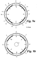
- Mikromechanischer Ring-Vibrationskreisel (101), der ein Ringelement (99) umfasst, das aus einem Material mit anisotropen mechanischen Eigenschaften hergestellt ist, dadurch gekennzeichnet, dass das Ringelement (99) dazu eingerichtet ist, während der Verwendung zu schwingen, und dadurch, dass wenigstens ein Bereich des Ringelements (99) relativ zu dem Rest des Ringelements verdickt ist, um die anisotropen mechanischen Eigenschaften des Materials zu kompensieren, aus dem das Ringelement (99) hergestellt ist.
- Vibrationskreisel nach Anspruch 1, bei dem wenigstens ein Bereich des Ringelements (99) relativ zum Rest des Ringelements auf eine solche Weise verdickt ist, dass die Dickenabmessung des Ringelements auf periodische Weise als Funktion der Winkeländerung um das Ringelement (99) herum variiert.
- Vibrationskreisel nach Anspruch 2, bei dem die periodische Variation um das Ringelement herum näherungsweise mit cos(4θ) auftritt, wobei θ die Winkeländerung um das Ringelement (99) herum ist.
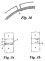
- Verfahren nach einem der vorangehenden Ansprüche, bei dem das Ringelement (99) durch eine Anzahl von Aufhängungsstegen (a-h) aufgehängt ist, die das Ringelement (99) mit einem Substrat (102) verbinden.
- Vibrationskreisel nach Anspruch 4, bei dem die Aufhängungsstege (a-h) mit einer äußeren Oberfläche des Ringelements (99) verbunden sind.
- Vibrationskreisel nach Anspruch 4, bei dem die Aufhängungsstege (a-h) mit einer inneren Oberfläche des Ringelements (99) verbunden sind
- Vibrationskreisel nach einem der Ansprüche 4 bis 6, bei dem die verdickten Abschnitte des Ringelements (99) ungefähr zwischen Paaren der Aufhängungsstege (a-h) auftreten.
- Vibrationskreisel nach einem der vorangehenden Ansprüche, bei dem das Ringelement (99) eine Platte von wenigstens einem Kondensator bildet, wobei der Vibrationskreisel derart eingerichtet ist, dass Bewegung des Ringelement (99) verursacht, dass der Wert des auf diese Weise gebildeten Kondensators variiert.
- Vibrationskreisel nach Anspruch 8, bei dem wenigstens eine Elektrode (D1, P1,2,3,4, S1,2,3) bereitgestellt ist, die eine zweite Platte des Kondensators bildet.
- Vibrationskreisel nach Anspruch 9, dadurch gekennzeichnet, dass die wenigstens eine Elektrode (D1, P1,2,3,4, S1,2,3) eine Antriebselektrode umfasst, die dazu eingerichtet ist, die Schwingungen des Ringelements (99) anzutreiben.
- Vibrationskreisel nach Anspruch 10, bei dem die Antriebselektrode dazu eingerichtet ist, das Ringelement (99) in einer ersten Schwingungsmode derart anzutreiben, dass es einen Schwingungsbauch mit Schwingungsmaximum gibt, der an die Antriebselektrode angrenzt.
- Vibrationskreisel nach Anspruch 11, bei dem wenigstens eine Sensorelektrode für die erste Mode bei ungefähr einem ganzzahligen Vielfachen von 90° um das Ringelement (99) herum ab der wenigstens einen Antriebselektrode bereitgestellt ist, wobei die wenigstens eine Sensorelektrode für die erste Mode dazu eingerichtet ist, Schwingungen der ersten Mode zu erfassen.
- Vibrationskreisel nach Anspruch 12, bei dem das Ringelement derart eingerichtet ist, dass es eine zweite Schwingungsmode aufweist, und wenigstens eine Sensorelektrode für die zweite Mode hat, die dazu eingerichtet ist, Schwingungen auf Grund der zweiten Schwingungsmode zu erfassen.
- Vibrationskreisel nach Anspruch 13, bei dem die Sensorelektrode für die zweite Mode an einem Knoten mit Bewegung durch die erste Schwingungsmode gleich Null angeordnet ist.
- Vibrationskreisel nach einem der vorangehenden Ansprüche, bei dem wenigstens ein Elektrodenpaar bereitgestellt ist, und das Ringelement dazu eingerichtet ist, zwischen dem Elektrodenpaar hindurchzulaufen.
- Vibrationskreisel nach Anspruch 15, bei dem wenigstens ein Paar von Elektroden dazu eingerichtet ist, ein erstes und ein zweites Signal zu erzeugen, und der Vibrationskreisel dazu eingerichtet ist, das erste und das zweite Signal differenziell zu verarbeiten.
- Vibrationskreisel nach einem der vorangehenden Ansprüche, der aus einem Material hergestellt ist, das Kristallebenen mit einer < 100>-Orientierung aufweist.
- Verfahren zur Herstellung eines mikromechanischen Ring-Vibrationskreisels (101), das die folgenden Schritte umfasst:(i) Nehmen einer Schicht aus kristallinem Material (102) mit anisotropen mechanischen Eigenschaften;(ii) Bestimmen des Grades der Fehlausrichtung des Kristallgitters innerhalb der Schicht aus dem Material (102), indem die exakte Kristallorientierung identifiziert wird;(iii) Berechnung des Grades der Änderung, die für die Dickenabmessung eines Ringelementes (99) erforderlich ist, das in der Schicht aus kristallinem Material (102) hergestellt ist, um die Fehlausrichtung des Kristallgitters zu kompensieren; und(iv) Herstellen eines solchen Ringelements (99) in der Schicht aus dem Material (102), wobei wenigstens ein Bereich des Ringelements (99) relativ zum Rest des Ringelements (99) verdickt ist, um die Fehlausrichtung und folglich die anisotropen mechanischen Eigenschaften der Schicht aus dem Material (102) zu kompensieren.
- Verfahren nach Anspruch 18, bei dem der Schritt (iv) der Herstellung eines Ringelements (99) die folgenden Schritte umfasst: Nehmen des ersten Wafers (2; 50) mit einer Isolierschicht (8, 10, 12, 14; 56), die darauf aufgebracht ist, und mit einem zweiten Wafer (4; 62), der mit der Isolierschicht (8, 10, 12, 14; 56) verbunden ist, unda) Aufbringen eines Musters auf und nachfolgendes Ätzen von entweder dem ersten oder dem zweiten Wafer, sodass Kanäle (18, 20; 52, 54) in dem einen Wafer (dem geätzten Wafer) erzeugt werden, die an der Grenze zu der Isolierschicht (8, 10, 12, 14; 56) enden; undb) Ätzen der Isolierschicht, um Teile der Isolierschicht (8, 10, 12, 14; 56) zu entfernen, die an den geätzten Wafer angrenzen, sodass die Teile des geätzten Wafers unterhalb einer zuvor festgelegten Größe, aufgehängte Teile, im wesentlichen frei über dem anderen Wafer aufgehängt werden.
- Verfahren nach Anspruch 19, bei dem die Isolierschicht eine Dicke zwischen 1,5µm und 3µm hat.
- Verfahren nach einem der Ansprüche 19 bis 20, bei dem das Verfahren die Masse der Teile unterhalb der zuvor festgelegten Größe erhöht, die während Schritt b) des Verfahrens im Wesentlichen freigelegt werden.
- Verfahren nach einem der Ansprüche 19 bis 21, bei dem die Maske für das Ätzen in Schritt a) optimiert ist, sodass Flächen, die geätzt werden sollen, im Wesentlichen gleiche Querschnittsflächen haben.
- Verfahren nach einem der Ansprüche 19 bis 22, bei dem Aufhängungsstege (a-h) vorgesehen sind, um die aufgehängten Teile mit dem Rest des geätzten Wafers zu verbinden.
- Verfahren nach einem der Ansprüche 19 bis 23, das weiter den Schritt des Reinigens der Ätzung der Isolierschicht (8, 10, 12, 14; 56) mit einem Dampf enthält.
- Verfahren nach einem der Ansprüche 19 bis 24, bei dem manche der Kanäle (8, 10, 12,14; 56), die in dem geätzten Wafer vor der Ausführung von Schritt b) erzeugt werden, mit einem Füllmaterial wieder aufgefüllt werden.
- Verfahren nach einem der Ansprüche 19 bis 25, bei dem Kontakte oder Verbindungsbahnen in die Isolierschicht eingebettet werden, wenn sie auf die Oberfläche des ersten Wafers (2; 50) aufgebracht wird.
- Verfahren nach einem der Ansprüche 19 bis 26, bei dem die Isolierschicht (8, 10, 12,14; 56) zwischen dem ersten und dem zweiten Wafer mehr als ein Material umfasst.
- Verfahren nach einem der Ansprüche 19 bis 27, bei dem die Materialien, aus denen die Isolierschicht (8, 10, 12, 14; 56) gebildet wird, Oxide des Materials sind, aus dem der Wafer hergestellt ist.
- Verfahren nach einem der Ansprüche 19 bis 28, bei dem eine Nitridschicht innerhalb der Isolierschicht nach Schritt b) zurückbleibt.
- Verfahren nach einem der Ansprüche 19 bis 29, bei dem die mechanische Spannung zwischen dem ersten und zweiten Wafer verringert wird, indem die Isolierschicht (8, 10, 12, 14; 56) als eine Reihe von Schichten bereitgestellt wird.
- Verfahren nach einem der Ansprüche 19 bis 30, bei dem die Dicke des geätzten Wafers zu Beginn des Prozesses b) im Wesentlichen im Bereich von 11 µm bis 200µm liegt.
- Verfahren nach Anspruch 18, bei dem der Schritt der Herstellung eines Ringelements (99) die folgenden Schritte umfasst:a. Aufbringen einer Isolierschicht (8, 10, 12, 14; 56) auf die oberste Oberfläche eines ersten Wafers (2; 50);b. Ätzen von Teilen der Isolierschicht (8, 10, 12, 14; 56);c. Verbinden eines zweiten Wafers (4; 62) mit der Isolierschicht (8, 10, 12, 14; 56); undd. Ätzen der untersten Oberfläche von einem der Wafer, dem geätzten Wafer, in Bereichen, die an die geätzten Teile der Isolierschicht (8, 10, 12,14; 56) angrenzen, sodass Teile des geätzten Wafers im Wesentlichen von dem Rest des ersten und zweiten Wafers frei werden (aufgehängte Teile).
- Verfahren nach Anspruch 32, bei dem der erste Wafer während Schritt d) nach dem Verfahren geätzt wird.
- Verfahren nach Anspruch 32 oder Anspruch 33, das einen weiteren Schritt zwischen den Schritten b) und c) umfasst, in dem die Teile der Isolierschicht, die geätzt wurden, mit einem Füllmaterial wiederaufgefüllt werden.
Priority Applications (1)
| Application Number | Priority Date | Filing Date | Title |
|---|---|---|---|
| EP07004839A EP1808672A3 (de) | 1998-09-12 | 1999-09-13 | Verbesserungen im Zusammenhang mit der Mikrobearbeitung |
Applications Claiming Priority (3)
| Application Number | Priority Date | Filing Date | Title |
|---|---|---|---|
| GBGB9819821.1A GB9819821D0 (en) | 1998-09-12 | 1998-09-12 | Improvements relating to micro-machining |
| GB9819821 | 1998-09-12 | ||
| PCT/GB1999/003028 WO2000016041A2 (en) | 1998-09-12 | 1999-09-13 | Formation of suspended beams using soi substrates, and application to the fabrication of a vibrating gyrometer |
Related Child Applications (1)
| Application Number | Title | Priority Date | Filing Date |
|---|---|---|---|
| EP07004839A Division EP1808672A3 (de) | 1998-09-12 | 1999-09-13 | Verbesserungen im Zusammenhang mit der Mikrobearbeitung |
Publications (2)
| Publication Number | Publication Date |
|---|---|
| EP1116008A2 EP1116008A2 (de) | 2001-07-18 |
| EP1116008B1 true EP1116008B1 (de) | 2007-07-18 |
Family
ID=10838709
Family Applications (2)
| Application Number | Title | Priority Date | Filing Date |
|---|---|---|---|
| EP07004839A Withdrawn EP1808672A3 (de) | 1998-09-12 | 1999-09-13 | Verbesserungen im Zusammenhang mit der Mikrobearbeitung |
| EP99946323A Expired - Lifetime EP1116008B1 (de) | 1998-09-12 | 1999-09-13 | Vibrationskreisels und sein herstellungsverfahren |
Family Applications Before (1)
| Application Number | Title | Priority Date | Filing Date |
|---|---|---|---|
| EP07004839A Withdrawn EP1808672A3 (de) | 1998-09-12 | 1999-09-13 | Verbesserungen im Zusammenhang mit der Mikrobearbeitung |
Country Status (11)
| Country | Link |
|---|---|
| US (2) | US6276205B1 (de) |
| EP (2) | EP1808672A3 (de) |
| JP (1) | JP4999227B2 (de) |
| KR (1) | KR100651769B1 (de) |
| AT (1) | ATE367570T1 (de) |
| AU (1) | AU5874099A (de) |
| CA (1) | CA2343446A1 (de) |
| DE (1) | DE69936590T2 (de) |
| GB (1) | GB9819821D0 (de) |
| NO (1) | NO20011230L (de) |
| WO (1) | WO2000016041A2 (de) |
Families Citing this family (67)
| Publication number | Priority date | Publication date | Assignee | Title |
|---|---|---|---|---|
| SE514042C2 (sv) * | 1998-05-08 | 2000-12-18 | Nordic Sensor Technologies Ab | Sensoranordning |
| AT409429B (de) * | 1999-07-15 | 2002-08-26 | Sez Semiconduct Equip Zubehoer | Verfahren zum ätzbehandeln von halbleitersubstraten zwecks freilegen einer metallschicht |
| US6803755B2 (en) | 1999-09-21 | 2004-10-12 | Rockwell Automation Technologies, Inc. | Microelectromechanical system (MEMS) with improved beam suspension |
| US6798312B1 (en) | 1999-09-21 | 2004-09-28 | Rockwell Automation Technologies, Inc. | Microelectromechanical system (MEMS) analog electrical isolator |
| WO2001025798A2 (en) * | 1999-10-05 | 2001-04-12 | L-3 Communications Corporation | A method for improving the performance of micromachined devices |
| US6456939B1 (en) * | 2000-01-04 | 2002-09-24 | Mccall Hiram | Micro inertial measurement unit |
| US6525352B1 (en) * | 2000-11-22 | 2003-02-25 | Network Photonics, Inc. | Method to reduce release time of micromachined devices |
| US6815243B2 (en) * | 2001-04-26 | 2004-11-09 | Rockwell Automation Technologies, Inc. | Method of fabricating a microelectromechanical system (MEMS) device using a pre-patterned substrate |
| US6761829B2 (en) | 2001-04-26 | 2004-07-13 | Rockwell Automation Technologies, Inc. | Method for fabricating an isolated microelectromechanical system (MEMS) device using an internal void |
| US6794271B2 (en) * | 2001-09-28 | 2004-09-21 | Rockwell Automation Technologies, Inc. | Method for fabricating a microelectromechanical system (MEMS) device using a pre-patterned bridge |
| US6756310B2 (en) * | 2001-09-26 | 2004-06-29 | Rockwell Automation Technologies, Inc. | Method for constructing an isolate microelectromechanical system (MEMS) device using surface fabrication techniques |
| KR100421217B1 (ko) * | 2001-05-30 | 2004-03-02 | 삼성전자주식회사 | 점착 방지 미세 구조물 제조 방법 |
| US6664786B2 (en) | 2001-07-30 | 2003-12-16 | Rockwell Automation Technologies, Inc. | Magnetic field sensor using microelectromechanical system |
| US6690178B2 (en) | 2001-10-26 | 2004-02-10 | Rockwell Automation Technologies, Inc. | On-board microelectromechanical system (MEMS) sensing device for power semiconductors |
| US6562642B1 (en) * | 2002-02-07 | 2003-05-13 | International Business Machines Corporation | Micro-structures and methods for their manufacture |
| GB0206509D0 (en) | 2002-03-20 | 2002-05-01 | Qinetiq Ltd | Micro-Electromechanical systems |
| GB0206510D0 (en) * | 2002-03-20 | 2002-05-01 | Qinetiq Ltd | Micro-Electromechanical systems |
| EP2386826B1 (de) * | 2002-06-10 | 2014-02-26 | Panasonic Corporation | Winkelgeschwindigkeitsmesser |
| FR2845200A1 (fr) * | 2002-09-26 | 2004-04-02 | Memscap | Procede de fabrication d'un composant electronique incluant une structure micro-electromecanique |
| KR100512988B1 (ko) * | 2002-09-26 | 2005-09-07 | 삼성전자주식회사 | 플렉서블 mems 트랜스듀서 제조방법 |
| US6979408B2 (en) * | 2002-12-30 | 2005-12-27 | Intel Corporation | Method and apparatus for photomask fabrication |
| US6975193B2 (en) * | 2003-03-25 | 2005-12-13 | Rockwell Automation Technologies, Inc. | Microelectromechanical isolating circuit |
| DE10331714B4 (de) * | 2003-07-11 | 2006-05-24 | Micronas Gmbh | Verfahren zur Strukturierung der Oberfläche eines Substrats |
| US20050062362A1 (en) * | 2003-08-28 | 2005-03-24 | Hongyuan Yang | Oscillatory gyroscope |
| US20050076866A1 (en) * | 2003-10-14 | 2005-04-14 | Hopper Mark L. | Electromechanical valve actuator |
| KR100605497B1 (ko) * | 2003-11-27 | 2006-07-28 | 삼성전자주식회사 | 에스오아이 기판들을 제조하는 방법들, 이를 사용하여반도체 소자들을 제조하는 방법들 및 그에 의해 제조된반도체 소자들 |
| TWI245902B (en) * | 2004-05-14 | 2005-12-21 | Chung Shan Inst Of Science | Microstructure angular velocity sensor device |
| CN1985149B (zh) | 2004-07-12 | 2010-11-03 | 住友精密工业株式会社 | 角速度传感器 |
| US20100117152A1 (en) * | 2007-06-28 | 2010-05-13 | Chang-Woo Oh | Semiconductor devices |
| KR100843717B1 (ko) * | 2007-06-28 | 2008-07-04 | 삼성전자주식회사 | 플로팅 바디 소자 및 벌크 바디 소자를 갖는 반도체소자 및그 제조방법 |
| KR100555569B1 (ko) | 2004-08-06 | 2006-03-03 | 삼성전자주식회사 | 절연막에 의해 제한된 채널영역을 갖는 반도체 소자 및 그제조방법 |
| KR100658202B1 (ko) | 2005-09-12 | 2006-12-15 | (주)마이크로인피니티 | 마이크로 구조물의 부양체 및 그 제조방법 |
| US7462509B2 (en) * | 2006-05-16 | 2008-12-09 | International Business Machines Corporation | Dual-sided chip attached modules |
| TWI305930B (en) * | 2006-06-19 | 2009-02-01 | Touch Micro System Tech | Method of fabricating suspended structure |
| US20080108224A1 (en) * | 2006-10-12 | 2008-05-08 | Zhaoning Yu | Patterning methods |
| US20100038825A1 (en) * | 2006-12-21 | 2010-02-18 | Mcdonald Joel P | Methods of forming microchannels by ultrafast pulsed laser direct-write processing |
| IL181367A (en) * | 2007-02-15 | 2013-03-24 | Elbit Systems Electro Optics Elop Ltd | Vibrating gyroscopic device for measuring angular velocity |
| US8056413B2 (en) * | 2007-09-11 | 2011-11-15 | Evigia Systems, Inc. | Sensor and sensing method utilizing symmetrical differential readout |
| ATE520960T1 (de) * | 2007-09-18 | 2011-09-15 | Atlantic Inertial Systems Ltd | Verbesserungen in bezug auf winkelgeschwindigkeitssensoren |
| EP2040032A1 (de) * | 2007-09-19 | 2009-03-25 | Atlantic Inertial Systems Limited | Verbesserungen bei oder im Zusammenhang mit Winkelgeschwindigkeitssensoren |
| US7992438B2 (en) * | 2007-11-28 | 2011-08-09 | Chung Shan Institute Of Science And Technology, Armaments Bureau, M.N.D. | Multiaxial gyroscope |
| US7908922B2 (en) * | 2008-01-24 | 2011-03-22 | Delphi Technologies, Inc. | Silicon integrated angular rate sensor |
| WO2009109969A2 (en) * | 2008-03-03 | 2009-09-11 | Ramot At Tel-Aviv University Ltd. | Micro scale mechanical rate sensors |
| US8451077B2 (en) | 2008-04-22 | 2013-05-28 | International Business Machines Corporation | MEMS switches with reduced switching voltage and methods of manufacture |
| GB0812788D0 (en) * | 2008-07-12 | 2008-08-20 | Atlantic Inertial Systems Ltd | Improvements in or relating to vibrating structure gyroscopes |
| US8263426B2 (en) | 2008-12-03 | 2012-09-11 | Electronics And Telecommunications Research Institute | High-sensitivity z-axis vibration sensor and method of fabricating the same |
| JP2012528335A (ja) * | 2009-05-27 | 2012-11-12 | キング アブドゥーラ ユニバーシティ オブ サイエンス アンド テクノロジー | 面外サスペンション方式を使用するmems質量−バネ−ダンパシステム |
| CN102472648B (zh) * | 2009-07-22 | 2014-04-16 | 皇家飞利浦电子股份有限公司 | 具有低响应时间和高灵敏度的热流量传感器集成电路 |
| US20120244969A1 (en) | 2011-03-25 | 2012-09-27 | May Patents Ltd. | System and Method for a Motion Sensing Device |
| JP5708222B2 (ja) * | 2011-05-12 | 2015-04-30 | 大日本印刷株式会社 | 力学量センサー |
| TWI456201B (zh) * | 2011-11-29 | 2014-10-11 | Univ Chung Hua | 無線式熱氣泡式加速儀及其製備方法 |
| US20130201316A1 (en) | 2012-01-09 | 2013-08-08 | May Patents Ltd. | System and method for server based control |
| US9006077B2 (en) * | 2013-08-21 | 2015-04-14 | GlobalFoundries, Inc. | Gate length independent silicon-on-nothing (SON) scheme for bulk FinFETs |
| JP6173851B2 (ja) | 2013-09-20 | 2017-08-02 | 株式会社日立ハイテクノロジーズ | 分析方法およびプラズマエッチング装置 |
| US9661215B2 (en) | 2014-04-22 | 2017-05-23 | Snapaid Ltd. | System and method for controlling a camera based on processing an image captured by other camera |
| EP2952979B1 (de) * | 2014-06-03 | 2017-03-01 | Nivarox-FAR S.A. | Uhrkomponente aus fotostrukturierbarem glas |
| EP3289430B1 (de) | 2015-04-27 | 2019-10-23 | Snap-Aid Patents Ltd. | Schätzung und verwendung einer relativen kopfhaltung und kamerasichtfeld |
| DE102015118346A1 (de) * | 2015-10-27 | 2017-04-27 | Endress+Hauser Flowtec Ag | MEMS Sensor zu Messung mindestens einer Messgröße |
| US11190374B2 (en) | 2017-08-28 | 2021-11-30 | Bright Data Ltd. | System and method for improving content fetching by selecting tunnel devices |
| EP4187881A1 (de) | 2017-08-28 | 2023-05-31 | Bright Data Ltd. | Verbesserung des abrufens von inhalten durch auswahl von tunnelvorrichtungen, die entsprechend einem geografischen standort gruppiert sind |
| EP3652721A1 (de) | 2017-09-04 | 2020-05-20 | NNG Software Developing and Commercial LLC | Verfahren und vorrichtung zum sammeln und verwenden von sensordaten von einem fahrzeug |
| KR102086230B1 (ko) * | 2018-06-26 | 2020-03-06 | 한국과학기술원 | 굴절률 및 스트레인의 주기적 동시변화를 이용한 공진기와 전하구속 구조 일체형 주기성 다리 구조 및 그 제조 방법 |
| EP3888346A4 (de) | 2019-02-19 | 2022-08-24 | Edgy Bees Ltd. | Schätzung der echtzeitverzögerung eines videodatenstroms |
| LT3780557T (lt) | 2019-02-25 | 2023-03-10 | Bright Data Ltd. | Turinio parsisiuntimo, naudojant url bandymų mechanizmą, sistema ir būdas |
| EP3935792A4 (de) | 2019-04-02 | 2022-11-30 | Bright Data Ltd. | System und verfahren zur verwaltung eines nichtdirekten url-abrufdienstes |
| CN109974681B (zh) * | 2019-04-09 | 2021-01-26 | 东南大学 | 一种基于光波导的盘式谐振陀螺仪及其加工封装方法 |
| WO2024042819A1 (ja) * | 2022-08-25 | 2024-02-29 | 住友精密工業株式会社 | 振動型角速度検出器 |
Family Cites Families (26)
| Publication number | Priority date | Publication date | Assignee | Title |
|---|---|---|---|---|
| JPS63202035A (ja) * | 1987-02-17 | 1988-08-22 | Mitsubishi Electric Corp | 半導体装置の製造方法 |
| US4968628A (en) | 1988-12-09 | 1990-11-06 | Harris Corporation | Method of fabricating back diffused bonded oxide substrates |
| US5238223A (en) * | 1989-08-11 | 1993-08-24 | Robert Bosch Gmbh | Method of making a microvalve |
| DE69218611T2 (de) * | 1991-06-12 | 1997-07-03 | Harris Corp | Verfahren zur herstellung eines halbleiter-beschleunigungsmessers |
| DE69232432T2 (de) | 1991-11-20 | 2002-07-18 | Canon Kk | Verfahren zur Herstellung einer Halbleiteranordnung |
| DE4309917A1 (de) | 1992-03-30 | 1993-10-07 | Awa Microelectronics | Verfahren zur Herstellung von Siliziummikrostrukturen sowie Siliziummikrostruktur |
| JP3367113B2 (ja) | 1992-04-27 | 2003-01-14 | 株式会社デンソー | 加速度センサ |
| CA2154357C (en) | 1993-02-04 | 2004-03-02 | Kevin A. Shaw | Microstructures and single-mask, single-crystal process for fabrication thereof |
| GB2276976B (en) | 1993-04-07 | 1996-10-23 | British Aerospace | Method of manufacturing a motion sensor |
| DE4315012B4 (de) | 1993-05-06 | 2007-01-11 | Robert Bosch Gmbh | Verfahren zur Herstellung von Sensoren und Sensor |
| US5324683A (en) | 1993-06-02 | 1994-06-28 | Motorola, Inc. | Method of forming a semiconductor structure having an air region |
| DE4332057A1 (de) | 1993-09-21 | 1995-03-30 | Siemens Ag | Integrierte mikromechanische Sensorvorrichtung und Verfahren zu deren Herstellung |
| US5415726A (en) | 1993-12-21 | 1995-05-16 | Delco Electronics Corporation | Method of making a bridge-supported accelerometer structure |
| US5511428A (en) | 1994-06-10 | 1996-04-30 | Massachusetts Institute Of Technology | Backside contact of sensor microstructures |
| US5495760A (en) * | 1994-07-05 | 1996-03-05 | Rockwell International Corporation | Beermug gyroscope |
| GB2292609B (en) | 1994-08-24 | 1998-04-15 | British Aerospace | Method for matching vibration mode frequencies on a vibrating structure |
| AU2683995A (en) | 1994-09-02 | 1996-03-27 | Stichting Voor De Technische Wetenschappen | Process for producing micromechanical structures by means of reactive ion etching |
| GB2299669B (en) * | 1995-04-07 | 1998-12-16 | British Aerospace | Method for actively balancing a vibrating structure gyroscope sensing element structure |
| JPH0914570A (ja) | 1995-06-27 | 1997-01-17 | Tokyo Gas Co Ltd | ライフライン管路の耐震強化装置 |
| JPH09145740A (ja) | 1995-09-22 | 1997-06-06 | Denso Corp | 加速度センサ |
| DE19537814B4 (de) | 1995-10-11 | 2009-11-19 | Robert Bosch Gmbh | Sensor und Verfahren zur Herstellung eines Sensors |
| US5721162A (en) | 1995-11-03 | 1998-02-24 | Delco Electronics Corporation | All-silicon monolithic motion sensor with integrated conditioning circuit |
| WO1997022140A2 (en) | 1995-11-29 | 1997-06-19 | Litton Systems, Inc. | Method for purging a multi-layer sacrificial etched silicon substrate |
| US6048774A (en) * | 1997-06-26 | 2000-04-11 | Denso Corporation | Method of manufacturing dynamic amount semiconductor sensor |
| US6075639A (en) * | 1997-10-22 | 2000-06-13 | The Board Of Trustees Of The Leland Stanford Junior University | Micromachined scanning torsion mirror and method |
| US6159385A (en) * | 1998-05-08 | 2000-12-12 | Rockwell Technologies, Llc | Process for manufacture of micro electromechanical devices having high electrical isolation |
-
1998
- 1998-09-12 GB GBGB9819821.1A patent/GB9819821D0/en not_active Ceased
- 1998-09-30 US US09/163,554 patent/US6276205B1/en not_active Expired - Lifetime
-
1999
- 1999-09-13 WO PCT/GB1999/003028 patent/WO2000016041A2/en active IP Right Grant
- 1999-09-13 AU AU58740/99A patent/AU5874099A/en not_active Abandoned
- 1999-09-13 CA CA002343446A patent/CA2343446A1/en not_active Abandoned
- 1999-09-13 KR KR1020017003168A patent/KR100651769B1/ko not_active IP Right Cessation
- 1999-09-13 DE DE69936590T patent/DE69936590T2/de not_active Expired - Lifetime
- 1999-09-13 JP JP2000570531A patent/JP4999227B2/ja not_active Expired - Fee Related
- 1999-09-13 EP EP07004839A patent/EP1808672A3/de not_active Withdrawn
- 1999-09-13 EP EP99946323A patent/EP1116008B1/de not_active Expired - Lifetime
- 1999-09-13 AT AT99946323T patent/ATE367570T1/de not_active IP Right Cessation
-
2001
- 2001-03-09 NO NO20011230A patent/NO20011230L/no not_active Application Discontinuation
- 2001-07-05 US US09/898,081 patent/US6670212B2/en not_active Expired - Fee Related
Also Published As
| Publication number | Publication date |
|---|---|
| WO2000016041A3 (en) | 2000-09-28 |
| US20020017132A1 (en) | 2002-02-14 |
| JP2002525843A (ja) | 2002-08-13 |
| CA2343446A1 (en) | 2000-03-23 |
| NO20011230L (no) | 2001-05-11 |
| WO2000016041A2 (en) | 2000-03-23 |
| JP4999227B2 (ja) | 2012-08-15 |
| US6276205B1 (en) | 2001-08-21 |
| EP1808672A2 (de) | 2007-07-18 |
| AU5874099A (en) | 2000-04-03 |
| KR100651769B1 (ko) | 2006-11-30 |
| DE69936590T2 (de) | 2007-11-22 |
| GB9819821D0 (en) | 1998-11-04 |
| EP1116008A2 (de) | 2001-07-18 |
| KR20010075052A (ko) | 2001-08-09 |
| ATE367570T1 (de) | 2007-08-15 |
| NO20011230D0 (no) | 2001-03-09 |
| US6670212B2 (en) | 2003-12-30 |
| EP1808672A3 (de) | 2009-06-17 |
| DE69936590D1 (de) | 2007-08-30 |
Similar Documents
| Publication | Publication Date | Title |
|---|---|---|
| EP1116008B1 (de) | Vibrationskreisels und sein herstellungsverfahren | |
| EP2083246B1 (de) | Integrierter Winkelgeschwindigkeitssensor aus Silikon | |
| Ayazi et al. | High aspect-ratio combined poly and single-crystal silicon (HARPSS) MEMS technology | |
| US7645627B2 (en) | Method for manufacturing a sensor device | |
| US6988408B2 (en) | Surface/bulk micromachined single-crystalline silicon micro-gyroscope | |
| US5535902A (en) | Gimballed vibrating wheel gyroscope | |
| EP0400939B1 (de) | Halbleiterwandler mit Schwingelement | |
| US7312553B2 (en) | Micromechanical component and method for producing same | |
| JP3037416B2 (ja) | マイクロメカニック式の回転値センサ | |
| Cho et al. | A high-Q birdbath resonator gyroscope (BRG) | |
| US11277112B2 (en) | Micro-electro-mechanical device with reduced temperature sensitivity and manufacturing method thereof | |
| EP3335004B1 (de) | Drehratensensoren | |
| US8443665B2 (en) | Frequency modulated micro gyro | |
| US6242276B1 (en) | Method for fabricating micro inertia sensor | |
| JP4362877B2 (ja) | 角速度センサ | |
| Ayazi et al. | High aspect-ratio dry-release poly-silicon MEMS technology for inertial-grade microgyroscopes | |
| US20020017133A1 (en) | Surface/bulk micromachined single-crystalline silicon micro-gyroscope | |
| JP2004004119A (ja) | 半導体力学量センサ | |
| JP4362739B2 (ja) | 振動型角速度センサ | |
| JP2002148278A (ja) | 半導体力学量センサとその製造方法 | |
| KR100233848B1 (ko) | 마이크로 자이로스코프 제조 방법 | |
| Piot et al. | Electromechanical and process design of a 3 axis piezoelectric MEMS gyro in GaAs |
Legal Events
| Date | Code | Title | Description |
|---|---|---|---|
| PUAI | Public reference made under article 153(3) epc to a published international application that has entered the european phase |
Free format text: ORIGINAL CODE: 0009012 |
|
| 17P | Request for examination filed |
Effective date: 20010310 |
|
| AK | Designated contracting states |
Kind code of ref document: A2 Designated state(s): AT BE CH CY DE DK ES FI FR GB GR IE IT LI LU MC NL PT SE |
|
| AX | Request for extension of the european patent |
Free format text: AL;LT;LV;MK;RO;SI |
|
| RAP1 | Party data changed (applicant data changed or rights of an application transferred) |
Owner name: QINETIQ LIMITED |
|
| 17Q | First examination report despatched |
Effective date: 20040809 |
|
| GRAP | Despatch of communication of intention to grant a patent |
Free format text: ORIGINAL CODE: EPIDOSNIGR1 |
|
| RTI1 | Title (correction) |
Free format text: VIBRATING GYROMETER AND ITS PROCESS OF FABRICATION |
|
| GRAS | Grant fee paid |
Free format text: ORIGINAL CODE: EPIDOSNIGR3 |
|
| GRAA | (expected) grant |
Free format text: ORIGINAL CODE: 0009210 |
|
| AK | Designated contracting states |
Kind code of ref document: B1 Designated state(s): AT BE CH CY DE DK ES FI FR GB GR IE IT LI LU MC NL PT SE |
|
| REG | Reference to a national code |
Ref country code: GB Ref legal event code: FG4D |
|
| REG | Reference to a national code |
Ref country code: CH Ref legal event code: EP |
|
| REF | Corresponds to: |
Ref document number: 69936590 Country of ref document: DE Date of ref document: 20070830 Kind code of ref document: P |
|
| REG | Reference to a national code |
Ref country code: CH Ref legal event code: NV Representative=s name: E. BLUM & CO. AG PATENT- UND MARKENANWAELTE VSP |
|
| REG | Reference to a national code |
Ref country code: IE Ref legal event code: FG4D |
|
| ET | Fr: translation filed | ||
| PG25 | Lapsed in a contracting state [announced via postgrant information from national office to epo] |
Ref country code: PT Free format text: LAPSE BECAUSE OF FAILURE TO SUBMIT A TRANSLATION OF THE DESCRIPTION OR TO PAY THE FEE WITHIN THE PRESCRIBED TIME-LIMIT Effective date: 20071218 Ref country code: NL Free format text: LAPSE BECAUSE OF FAILURE TO SUBMIT A TRANSLATION OF THE DESCRIPTION OR TO PAY THE FEE WITHIN THE PRESCRIBED TIME-LIMIT Effective date: 20070718 Ref country code: ES Free format text: LAPSE BECAUSE OF FAILURE TO SUBMIT A TRANSLATION OF THE DESCRIPTION OR TO PAY THE FEE WITHIN THE PRESCRIBED TIME-LIMIT Effective date: 20071029 |
|
| NLV1 | Nl: lapsed or annulled due to failure to fulfill the requirements of art. 29p and 29m of the patents act | ||
| PG25 | Lapsed in a contracting state [announced via postgrant information from national office to epo] |
Ref country code: AT Free format text: LAPSE BECAUSE OF FAILURE TO SUBMIT A TRANSLATION OF THE DESCRIPTION OR TO PAY THE FEE WITHIN THE PRESCRIBED TIME-LIMIT Effective date: 20070718 |
|
| PG25 | Lapsed in a contracting state [announced via postgrant information from national office to epo] |
Ref country code: BE Free format text: LAPSE BECAUSE OF FAILURE TO SUBMIT A TRANSLATION OF THE DESCRIPTION OR TO PAY THE FEE WITHIN THE PRESCRIBED TIME-LIMIT Effective date: 20070718 |
|
| PG25 | Lapsed in a contracting state [announced via postgrant information from national office to epo] |
Ref country code: MC Free format text: LAPSE BECAUSE OF NON-PAYMENT OF DUE FEES Effective date: 20070930 Ref country code: GR Free format text: LAPSE BECAUSE OF FAILURE TO SUBMIT A TRANSLATION OF THE DESCRIPTION OR TO PAY THE FEE WITHIN THE PRESCRIBED TIME-LIMIT Effective date: 20071019 Ref country code: DK Free format text: LAPSE BECAUSE OF FAILURE TO SUBMIT A TRANSLATION OF THE DESCRIPTION OR TO PAY THE FEE WITHIN THE PRESCRIBED TIME-LIMIT Effective date: 20070718 |
|
| PLBE | No opposition filed within time limit |
Free format text: ORIGINAL CODE: 0009261 |
|
| STAA | Information on the status of an ep patent application or granted ep patent |
Free format text: STATUS: NO OPPOSITION FILED WITHIN TIME LIMIT |
|
| 26N | No opposition filed |
Effective date: 20080421 |
|
| PG25 | Lapsed in a contracting state [announced via postgrant information from national office to epo] |
Ref country code: SE Free format text: LAPSE BECAUSE OF FAILURE TO SUBMIT A TRANSLATION OF THE DESCRIPTION OR TO PAY THE FEE WITHIN THE PRESCRIBED TIME-LIMIT Effective date: 20071018 |
|
| PG25 | Lapsed in a contracting state [announced via postgrant information from national office to epo] |
Ref country code: IE Free format text: LAPSE BECAUSE OF NON-PAYMENT OF DUE FEES Effective date: 20070913 |
|
| PG25 | Lapsed in a contracting state [announced via postgrant information from national office to epo] |
Ref country code: CY Free format text: LAPSE BECAUSE OF FAILURE TO SUBMIT A TRANSLATION OF THE DESCRIPTION OR TO PAY THE FEE WITHIN THE PRESCRIBED TIME-LIMIT Effective date: 20070718 |
|
| PG25 | Lapsed in a contracting state [announced via postgrant information from national office to epo] |
Ref country code: LU Free format text: LAPSE BECAUSE OF NON-PAYMENT OF DUE FEES Effective date: 20070913 |
|
| PGFP | Annual fee paid to national office [announced via postgrant information from national office to epo] |
Ref country code: FI Payment date: 20090915 Year of fee payment: 11 Ref country code: CH Payment date: 20090923 Year of fee payment: 11 |
|
| PG25 | Lapsed in a contracting state [announced via postgrant information from national office to epo] |
Ref country code: IT Free format text: LAPSE BECAUSE OF NON-PAYMENT OF DUE FEES Effective date: 20070930 |
|
| REG | Reference to a national code |
Ref country code: CH Ref legal event code: PL |
|
| PG25 | Lapsed in a contracting state [announced via postgrant information from national office to epo] |
Ref country code: FI Free format text: LAPSE BECAUSE OF NON-PAYMENT OF DUE FEES Effective date: 20100913 |
|
| PG25 | Lapsed in a contracting state [announced via postgrant information from national office to epo] |
Ref country code: LI Free format text: LAPSE BECAUSE OF NON-PAYMENT OF DUE FEES Effective date: 20100930 Ref country code: CH Free format text: LAPSE BECAUSE OF NON-PAYMENT OF DUE FEES Effective date: 20100930 |
|
| PGFP | Annual fee paid to national office [announced via postgrant information from national office to epo] |
Ref country code: GB Payment date: 20120920 Year of fee payment: 14 |
|
| PGFP | Annual fee paid to national office [announced via postgrant information from national office to epo] |
Ref country code: DE Payment date: 20120921 Year of fee payment: 14 |
|
| PGFP | Annual fee paid to national office [announced via postgrant information from national office to epo] |
Ref country code: FR Payment date: 20121010 Year of fee payment: 14 |
|
| GBPC | Gb: european patent ceased through non-payment of renewal fee |
Effective date: 20130913 |
|
| REG | Reference to a national code |
Ref country code: DE Ref legal event code: R119 Ref document number: 69936590 Country of ref document: DE Effective date: 20140401 |
|
| REG | Reference to a national code |
Ref country code: FR Ref legal event code: ST Effective date: 20140530 |
|
| PG25 | Lapsed in a contracting state [announced via postgrant information from national office to epo] |
Ref country code: GB Free format text: LAPSE BECAUSE OF NON-PAYMENT OF DUE FEES Effective date: 20130913 |
|
| PG25 | Lapsed in a contracting state [announced via postgrant information from national office to epo] |
Ref country code: FR Free format text: LAPSE BECAUSE OF NON-PAYMENT OF DUE FEES Effective date: 20130930 Ref country code: DE Free format text: LAPSE BECAUSE OF NON-PAYMENT OF DUE FEES Effective date: 20140401 |