EP1111970B1 - Schaltungsplatte für Hochspannungseinsatz - Google Patents
Schaltungsplatte für Hochspannungseinsatz Download PDFInfo
- Publication number
- EP1111970B1 EP1111970B1 EP00307630A EP00307630A EP1111970B1 EP 1111970 B1 EP1111970 B1 EP 1111970B1 EP 00307630 A EP00307630 A EP 00307630A EP 00307630 A EP00307630 A EP 00307630A EP 1111970 B1 EP1111970 B1 EP 1111970B1
- Authority
- EP
- European Patent Office
- Prior art keywords
- end portion
- insulating
- circuit board
- circuit pattern
- voltage
- Prior art date
- Legal status (The legal status is an assumption and is not a legal conclusion. Google has not performed a legal analysis and makes no representation as to the accuracy of the status listed.)
- Expired - Lifetime
Links
Images


Classifications
-
- H—ELECTRICITY
- H05—ELECTRIC TECHNIQUES NOT OTHERWISE PROVIDED FOR
- H05K—PRINTED CIRCUITS; CASINGS OR CONSTRUCTIONAL DETAILS OF ELECTRIC APPARATUS; MANUFACTURE OF ASSEMBLAGES OF ELECTRICAL COMPONENTS
- H05K3/00—Apparatus or processes for manufacturing printed circuits
- H05K3/22—Secondary treatment of printed circuits
-
- H—ELECTRICITY
- H05—ELECTRIC TECHNIQUES NOT OTHERWISE PROVIDED FOR
- H05K—PRINTED CIRCUITS; CASINGS OR CONSTRUCTIONAL DETAILS OF ELECTRIC APPARATUS; MANUFACTURE OF ASSEMBLAGES OF ELECTRICAL COMPONENTS
- H05K1/00—Printed circuits
- H05K1/02—Details
- H05K1/0213—Electrical arrangements not otherwise provided for
- H05K1/0254—High voltage adaptations; Electrical insulation details; Overvoltage or electrostatic discharge protection ; Arrangements for regulating voltages or for using plural voltages
- H05K1/0257—Overvoltage protection
-
- H—ELECTRICITY
- H01—ELECTRIC ELEMENTS
- H01L—SEMICONDUCTOR DEVICES NOT COVERED BY CLASS H10
- H01L23/00—Details of semiconductor or other solid state devices
- H01L23/34—Arrangements for cooling, heating, ventilating or temperature compensation ; Temperature sensing arrangements
- H01L23/36—Selection of materials, or shaping, to facilitate cooling or heating, e.g. heatsinks
- H01L23/373—Cooling facilitated by selection of materials for the device or materials for thermal expansion adaptation, e.g. carbon
- H01L23/3735—Laminates or multilayers, e.g. direct bond copper ceramic substrates
-
- H—ELECTRICITY
- H01—ELECTRIC ELEMENTS
- H01L—SEMICONDUCTOR DEVICES NOT COVERED BY CLASS H10
- H01L2924/00—Indexing scheme for arrangements or methods for connecting or disconnecting semiconductor or solid-state bodies as covered by H01L24/00
- H01L2924/0001—Technical content checked by a classifier
- H01L2924/0002—Not covered by any one of groups H01L24/00, H01L24/00 and H01L2224/00
-
- H—ELECTRICITY
- H05—ELECTRIC TECHNIQUES NOT OTHERWISE PROVIDED FOR
- H05K—PRINTED CIRCUITS; CASINGS OR CONSTRUCTIONAL DETAILS OF ELECTRIC APPARATUS; MANUFACTURE OF ASSEMBLAGES OF ELECTRICAL COMPONENTS
- H05K1/00—Printed circuits
- H05K1/02—Details
- H05K1/03—Use of materials for the substrate
- H05K1/0306—Inorganic insulating substrates, e.g. ceramic, glass
-
- H—ELECTRICITY
- H05—ELECTRIC TECHNIQUES NOT OTHERWISE PROVIDED FOR
- H05K—PRINTED CIRCUITS; CASINGS OR CONSTRUCTIONAL DETAILS OF ELECTRIC APPARATUS; MANUFACTURE OF ASSEMBLAGES OF ELECTRICAL COMPONENTS
- H05K2201/00—Indexing scheme relating to printed circuits covered by H05K1/00
- H05K2201/01—Dielectrics
- H05K2201/0137—Materials
- H05K2201/0175—Inorganic, non-metallic layer, e.g. resist or dielectric for printed capacitor
-
- H—ELECTRICITY
- H05—ELECTRIC TECHNIQUES NOT OTHERWISE PROVIDED FOR
- H05K—PRINTED CIRCUITS; CASINGS OR CONSTRUCTIONAL DETAILS OF ELECTRIC APPARATUS; MANUFACTURE OF ASSEMBLAGES OF ELECTRICAL COMPONENTS
- H05K2201/00—Indexing scheme relating to printed circuits covered by H05K1/00
- H05K2201/03—Conductive materials
- H05K2201/0332—Structure of the conductor
- H05K2201/0335—Layered conductors or foils
- H05K2201/0355—Metal foils
-
- H—ELECTRICITY
- H05—ELECTRIC TECHNIQUES NOT OTHERWISE PROVIDED FOR
- H05K—PRINTED CIRCUITS; CASINGS OR CONSTRUCTIONAL DETAILS OF ELECTRIC APPARATUS; MANUFACTURE OF ASSEMBLAGES OF ELECTRICAL COMPONENTS
- H05K2201/00—Indexing scheme relating to printed circuits covered by H05K1/00
- H05K2201/09—Shape and layout
- H05K2201/09145—Edge details
-
- H—ELECTRICITY
- H05—ELECTRIC TECHNIQUES NOT OTHERWISE PROVIDED FOR
- H05K—PRINTED CIRCUITS; CASINGS OR CONSTRUCTIONAL DETAILS OF ELECTRIC APPARATUS; MANUFACTURE OF ASSEMBLAGES OF ELECTRICAL COMPONENTS
- H05K2201/00—Indexing scheme relating to printed circuits covered by H05K1/00
- H05K2201/09—Shape and layout
- H05K2201/09209—Shape and layout details of conductors
- H05K2201/09654—Shape and layout details of conductors covering at least two types of conductors provided for in H05K2201/09218 - H05K2201/095
- H05K2201/098—Special shape of the cross-section of conductors, e.g. very thick plated conductors
-
- H—ELECTRICITY
- H05—ELECTRIC TECHNIQUES NOT OTHERWISE PROVIDED FOR
- H05K—PRINTED CIRCUITS; CASINGS OR CONSTRUCTIONAL DETAILS OF ELECTRIC APPARATUS; MANUFACTURE OF ASSEMBLAGES OF ELECTRICAL COMPONENTS
- H05K2203/00—Indexing scheme relating to apparatus or processes for manufacturing printed circuits covered by H05K3/00
- H05K2203/03—Metal processing
- H05K2203/0346—Deburring, rounding, bevelling or smoothing conductor edges
-
- H—ELECTRICITY
- H05—ELECTRIC TECHNIQUES NOT OTHERWISE PROVIDED FOR
- H05K—PRINTED CIRCUITS; CASINGS OR CONSTRUCTIONAL DETAILS OF ELECTRIC APPARATUS; MANUFACTURE OF ASSEMBLAGES OF ELECTRICAL COMPONENTS
- H05K2203/00—Indexing scheme relating to apparatus or processes for manufacturing printed circuits covered by H05K3/00
- H05K2203/10—Using electric, magnetic and electromagnetic fields; Using laser light
- H05K2203/105—Using an electrical field; Special methods of applying an electric potential
-
- H—ELECTRICITY
- H05—ELECTRIC TECHNIQUES NOT OTHERWISE PROVIDED FOR
- H05K—PRINTED CIRCUITS; CASINGS OR CONSTRUCTIONAL DETAILS OF ELECTRIC APPARATUS; MANUFACTURE OF ASSEMBLAGES OF ELECTRICAL COMPONENTS
- H05K2203/00—Indexing scheme relating to apparatus or processes for manufacturing printed circuits covered by H05K3/00
- H05K2203/10—Using electric, magnetic and electromagnetic fields; Using laser light
- H05K2203/107—Using laser light
-
- H—ELECTRICITY
- H05—ELECTRIC TECHNIQUES NOT OTHERWISE PROVIDED FOR
- H05K—PRINTED CIRCUITS; CASINGS OR CONSTRUCTIONAL DETAILS OF ELECTRIC APPARATUS; MANUFACTURE OF ASSEMBLAGES OF ELECTRICAL COMPONENTS
- H05K2203/00—Indexing scheme relating to apparatus or processes for manufacturing printed circuits covered by H05K3/00
- H05K2203/12—Using specific substances
- H05K2203/128—Molten metals, e.g. casting thereof, or melting by heating and excluding molten solder
-
- H—ELECTRICITY
- H05—ELECTRIC TECHNIQUES NOT OTHERWISE PROVIDED FOR
- H05K—PRINTED CIRCUITS; CASINGS OR CONSTRUCTIONAL DETAILS OF ELECTRIC APPARATUS; MANUFACTURE OF ASSEMBLAGES OF ELECTRICAL COMPONENTS
- H05K3/00—Apparatus or processes for manufacturing printed circuits
- H05K3/22—Secondary treatment of printed circuits
- H05K3/24—Reinforcing the conductive pattern
- H05K3/244—Finish plating of conductors, especially of copper conductors, e.g. for pads or lands
-
- H—ELECTRICITY
- H05—ELECTRIC TECHNIQUES NOT OTHERWISE PROVIDED FOR
- H05K—PRINTED CIRCUITS; CASINGS OR CONSTRUCTIONAL DETAILS OF ELECTRIC APPARATUS; MANUFACTURE OF ASSEMBLAGES OF ELECTRICAL COMPONENTS
- H05K3/00—Apparatus or processes for manufacturing printed circuits
- H05K3/38—Improvement of the adhesion between the insulating substrate and the metal
-
- Y—GENERAL TAGGING OF NEW TECHNOLOGICAL DEVELOPMENTS; GENERAL TAGGING OF CROSS-SECTIONAL TECHNOLOGIES SPANNING OVER SEVERAL SECTIONS OF THE IPC; TECHNICAL SUBJECTS COVERED BY FORMER USPC CROSS-REFERENCE ART COLLECTIONS [XRACs] AND DIGESTS
- Y10—TECHNICAL SUBJECTS COVERED BY FORMER USPC
- Y10T—TECHNICAL SUBJECTS COVERED BY FORMER US CLASSIFICATION
- Y10T29/00—Metal working
- Y10T29/49—Method of mechanical manufacture
- Y10T29/49002—Electrical device making
- Y10T29/49117—Conductor or circuit manufacturing
- Y10T29/49124—On flat or curved insulated base, e.g., printed circuit, etc.
- Y10T29/49155—Manufacturing circuit on or in base
- Y10T29/49156—Manufacturing circuit on or in base with selective destruction of conductive paths
Definitions
- the present invention relates to a method of manufacturing an insulating substrate which can secure an insulation within a package such as a power semiconductor apparatus, and more particularly to an insulating circuit board intended to improve an insulating property of a composite member comprising an insulating substrate and an electrode conductor bonded to the insulating substrate by a bonding member, and a power semiconductor apparatus employing the insulating circuit board.
- a semiconductor apparatus which is composed by sealing a semiconductor device, such as an IGBT, a diode, a GTO, a transistor or the like, within an insulating container.
- the apparatus is applied to various kinds of inverter apparatus or the like in accordance with its voltage resistance property and its current capacity.
- the apparatus is composed so as to insulate an electric circuit from a base via an insulating substrate such as an alumina (Al 2 O 3 ), an aluminum nitride (AlN) or the like within the apparatus, thereby improving easiness of mounting.
- the IGBT has advantages of an easy control and a high frequency operation with a great amount of current, since the IGBT is a voltage control type device.
- the IGBT device is developed to have a great capacity, so that the performance thereof is improved up to a field covered by the conventional GTO.
- an area of the insulating substrate used within the apparatus becomes large due to an increase of size and an increases of the number of chips of the semiconductor device used within the apparatus.
- a method of providing a terraced portion (a step portion) in an end portion of a conductive layer bonded to the insulating substrate as shown in Japanese Patent Publication No.
- an average electric field strength is reduced by, in general, a method of increasing a thickness of the insulating substrate so as to reduce the electric field strength, or a method of increasing a creepage distance between the circuit pattern and an end portion of the insulating substrate.
- a whole of the insulating circuit board in the semiconductor apparatus is covered with an organic resin such as a silicone gel.
- an organic resin such as a silicone gel.
- a partial electric discharge is generated in an electric field concentrating portion having a local great electric field strength as a precursor phenomenon of a dielectric breakdown, thereby a void or an electric tree is generated.
- the electric discharge is continuously generated, so that there is a risk that the tree grows to generate the dielectric breakdown.
- the heat conduction of the insulating substrate is smaller than that of the electrode conductor (for example, a thermal conductivity coefficient of a copper generally used as an electrode conductor is 398 W/mK and on the contrary, those of an alumina and AlN used as an insulating substrate are 36 W/mK and 175 W/mK respectively, which are one half or less of that of a copper), a heat resistance of the apparatus is increased. Further, the method of increasing the creepage distance so as to improve the withstand voltage makes the apparatus large.
- the present invention seeks to provide an insulating circuit board having a high withstand voltage (corresponding to a partial electric discharge starting voltage and a breakdown voltage), and to provide a power semiconductor apparatus having a high insulating reliability by using the insulating circuit board.
- a method of manufacturing an insulating circuit board comprising the step of:
- a method of manufacturing an insulating circuit board comprising the steps of:
- an insulating circuit board comprising:
- US-A-5986218 discloses a circuit board in which conductive layers are formed on opposed surfaces of the insulating substrate.
- the conductive layers form electrodes and have an edge with a curvature radius of 0.1 ⁇ m.
- an insulating circuit board having an insulating substrate, and an electrode conductor bonded to a surface of the insulating substrate by a bonding member to form a circuit pattern on the surface of the insulating substrate, characterised in that:
- the invention may also provide a power semiconductor apparatus using the insulating circuit board of the third or fourth aspects.
- a direct voltage may be applied to the circuit pattern in the atmospheric or depressurized gas so as to allow the conductor end portion to discharge electricity at one or more times per one second.
- a voltage may be applied to the circuit pattern by using a circuit having a resistance connected to the circuit pattern in series so as to allow the conductor end portion to discharge electricity.
- the conductor end portion of the circuit pattern may be melted and re-solidified by laser beam irradiation.
- the voltage may be applied and electrically discharged before coating an organic resin such as a silicone gel or the like. Further, since the electric discharge energy is concentrated near the electric discharge portion even in the case of the electric discharge at a relatively low voltage, it is possible to obtain an effect sufficient to melt and deform the conductor metal.
- Fig. 1 shows a method of manufacturing an insulating circuit board in accordance with an embodiment of the present invention.
- the manufacturing process in accordance with the present embodiment has steps (a) to (e) shown in Fig. 1.
- steps (a) to (e) shown in Fig. 1 At first, in a step (a), in order to bond an electrode board 3 made of a Cu foil to an AlN insulating substrate 1, a brazing member 2 made of Cu-Ag-Ti alloy, for example, is applied in accordance with a pattern printing.
- a step (b) after setting the Cu foil 3, a bonding operation is performed by thermally treating at about 800°C while applying a load by a weight or the like.
- the N contained in the AlN insulating circuit board 1 and the Ti contained in the Cu-Ag-Ti alloy brazing member 2 are reacted to produce a TiN reaction layer 4.
- the TiN reaction layer 4 is also formed in a portion of a brazing member 5 melting and flowing out from the first printing area of the Cu-Ag-Ti alloy brazing member 2.
- a Ni plating 6 in a step (d) is applied as it is.
- the conductor layer portion required for improving a heat cycle resistance is masked and the flowing out brazing member 5 is etched and removed.
- the insulating circuit board produced by the steps (a) to (d) is referred as a comparative embodiment.
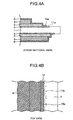
- Figs. 2A and 2B show the comparative embodiment, that is, the insulating circuit board obtained after the step (d), and Figs. 3A and 3B show an enlarged view of the end portion of the conductor electrode of the insulating circuit board.
- Figs. 2A and 3A are cross sectional views of the insulating circuit board and Figs. 2B and 3B are plan views of the insulating circuit board as viewed from an upper portion.
- the Ni plating 6 is also partially attached onto the TiN reaction layer 4, and the thin layer 7 constituted only the Ni plating is formed in the end portion of the conductor electrode.
- a curvature radius of an end portion lla of a conductor electrode at a distal end in the thin layer constituted only by the Ni plating is 3 ⁇ m or less, for example, as shown in Fig. 3A.
- the top elevational view in Fig. 2B shows a shape of a portion in which the brazing member flows out.
- a shape of the brazing member terminal end is determined by the flowing out of the brazing member and an etched shape. Accordingly, it is hard to form a flat shape with evenness, so that the end portion of the conductor electrode becomes an unevenness 12 having a projection shape 11b, for example.
- a difference "d" between a cape and a recess of the uneven portion in the end portion of the conductor electrode is 50 ⁇ m or more, as shown in Fig. 3B.
- a partial electric discharge is generated from a portion such as the projection-shaped distal end lla or the like of the end portion of the conductor electrode in which an electric field is concentrated. Accordingly, there is a possibility that a tree 13 and a void 14 is generated in the organic seal resin such as a silicone gel or the like and a deterioration is promoted.
- the test voltage means a maximum voltage applied in a withstand voltage test or the like performed before shipping the products.
- a step (e) in Fig. 1 is added. That is, before assembling the insulating circuit board into the semiconductor apparatus, a voltage is applied to the circuit pattern in the atmospheric air or the pressure reduced gas so as to allow the circuit pattern to discharge electricity 10 by using a power source 8, and an acute shape of the end portion of the conductor electrode is melted and re-solidified by the electric discharge energy, thereby being smoothly deformed.
- a resistance connected to the circuit pattern in series restricts an electric discharge current flowing at a time of the electric discharge, and is used for preventing a short circuit phenomenon (and a carbonized conductive passage formation due to the short circuit) between the circuit patterns due to the electric discharge and controlling a melting degree of the end portion of the conductor electrode.
- Figs. 4A and 4B show an insulating circuit board in accordance with an embodiment of the present invention
- Figs. 5A and 5B show an enlarged view of the end portion of the conductor electrode thereof.
- Figs. 4A and 5A are cross sectional views of the insulating circuit board
- Figs. 4B and 5B are plan views of the insulating circuit board as viewed from an upper portion.
- Fig. 6 shows an example of a voltage waveform obtained by applying an alternating voltage 16 having a commercial power source frequency (50 Hz) to the circuit pattern of the insulating circuit board in accordance with the present invention so as to electrically discharge at substantially each of cycles.
- one cycle means one period in the alternating voltage.
- an alternating voltage 16 is applied between the patterns on the insulating circuit board or between the patterns on the front side and the back side of the insulating circuit board so as to allow the circuit pattern to discharge electricity 17 at substantially each of cycles as shown in Fig. 6, thereby projection shapes 11a and 11b of the end portions of the conductor electrode are melted and re-solidified by the electric discharge energy so as to be smoothened.
- an alternating voltage of 3 kV to 5 kV is applied between the front and back electrodes for a thirty seconds to five minutes so as to electrically discharge at substantially each of cycles.
- the curvature radius of the end portion 11a of the conductor electrode is increased in comparison with the insulating circuit board in accordance with the comparative embodiment in Fig. 3A, for example, it is set to be equal to or more than 3 ⁇ m as denoted by reference symbol 15a.
- the unevenness 12 in the end portion of the conductor electrode, which has the projection shape 11b, is reduced so as to form a smooth shape as denoted by reference symbol 15b.
- the structure is formed such that the difference "d" between the cape and the recess of the end portion of the conductor electrode is equal to or less than 50 ⁇ m.
- Fig. 7 shows a relation between a curvature radius of the electrode end portion and a partial electric discharge starting voltage.
- the curvature radius of the electrode end portion is preferably set to be 3 ⁇ m or more.
- the larger the curvature radius of the electrode end portion is made as shown in Fig. 7, the more the electric field concentration is reduced, so that the partial electric discharge starting voltage is improved.
- the curvature radius of the electrode end portion is set to be 5 ⁇ m or more.
- Fig. 8 shows a relation between the difference between the cape and the recess in the projection portion of the electrode end portion and the partial electric discharge starting voltage.
- the shape of the electrode end portion becomes smooth by being melted and re-solidified due to the electric discharge, it is possible to reduce the concentration of the electric field in the end portion of the conductor electrode and the local strength of the electric field, whereby it is possible to increase the partial electric discharge starting voltage.
- alternating voltage having the commercial power source frequency 50 Hz or 60 Hz
- the same effects can be obtained by the alternating voltage having any frequency or by a direct voltage application.
- Fig. 9 shows a relation between the electric discharge frequency and the treated result (the partial electric discharge starting voltage) by applying the alternating voltage application
- Fig. 10 shows a relation between the number of the electric discharge per one second and the treated result (the partial electric discharge starting voltage) by applying the direct voltage application.
- the partial electric discharge starting voltage is improved by discharging, however, in order to obtain the effect, it is desirable to electrically discharge 0.2 times or more per one cycle. More desirably, it is preferable to electrically discharge at substantially each cycle (which means 0.8 times or more per one cycle).
- the partial electric discharge starting voltage is improved as shown in Fig. 10 by applying about 1.4 times voltage value of the alternating voltage so as to electrically discharge. In order to obtain the effects, 0.2 times or more per one second is desirable, and more desirably, it is preferable to electrically discharge one time or more per one second.
- Fig. 11 shows a relation between an air pressure and a minimum electric discharge voltage in the case of applying the voltage in the atmospheric air and the pressure reduced gas so as to electrically discharge.
- the electric discharge is generated at about 2 kV under the reduced pressure, for example under 1000 Pa, however, in the atmospheric air (1.013 x 10 5 Pa), the electric discharge is generated only at about 3 kV or more.
- Fig. 12 shows the air pressure and an effect obtained by the electric discharge (the partial electric discharge starting voltage after assembling in the semiconductor).
- the effect is great in the atmospheric air but small under the reduced pressure.
- the electric discharge aspect moves to an area of a low electric current glow discharge under the reduced pressure. Accordingly, 10 3 Pa or more is desirable for a range of the air pressure, and more desirably, from 10 4 Pa to the atmospheric pressure is preferable.
- a treating time (a time for applying the voltage onto the circuit pattern) may be set to be 10 minutes or less.
- Fig. 13 shows a relation between a voltage, a current and a treating time (a voltage applying time) which are applied to the circuit pattern on the insulating circuit board in accordance with the present invention, and the effect thereof.
- Fig. 13A shows a relation between the voltage applied to the circuit pattern and the partial electric discharge starting voltage.
- the electric discharge frequency is increased and thus the end portion of the conductor electrode becomes easily melted, such that the effect is increased and the partial electric discharge starting voltage is improved.
- Figs. 13A-13C there is shown the results obtained under the condition that the thickness of the insulating circuit board is 0.635 mm and under the atmospheric air.
- the electric discharge is generated when the voltage is 3 kV or more, and the effect is increased according to the increase of the voltage.
- the electric discharge is generated from about 1 kV under the reduced pressure, and the effect is increased in accordance with the increase of the voltage in the same manner.
- the value of the voltage applied to the circuit pattern is desirably in a range between 1 kV and 8 kV.
- Fig. 13B shows a relation between the electric discharge current and the partial electric discharge starting voltage.
- Fig. 13C shows a relation between the treating time (the voltage applying time) and the effect thereof.
- the longer the treating time is the higher the effect can be obtained.
- the treating time is increased to a certain degree, the projection shapes 11a and 11b are reduced (namely, in smooth) and the effect is saturated.
- the treating time is desirably set to be 10 minutes or less, preferably, about 1 to 5 minutes.
- the inert gas since it is possible to prevent the oxidization, this rule can not applied.
- a laser beam in order to melt the end portion of the conductor electrode, in addition to utilizing the electric discharge energy, it is possible to irradiate a laser beam so that the end portion of the conductor electrode is melted and re-solidified due to the energy thereof.
- a laser to be used there can be listed up a carbon dioxide (CO 2 ) gas laser, a YAG laser, an excimer laser or the like. Some hundreds watt of laser output is sufficient for melting only the end portion of the conductor electrode, and the laser is irradiated to the end portion of the conductor electrode so that an energy density becomes 10 5 W/cm 2 or less.
- the energy density becomes higher than 10 6 W/cm 2
- the melted conductor is sputtered, thereby giving a bad influence to the insulating substrate.
- the circuit pattern is largely oxidized due to the melting by the laser beam, it is possible to shield by the inert gas so as to prevent the oxidization.
Landscapes
- Engineering & Computer Science (AREA)
- Microelectronics & Electronic Packaging (AREA)
- Manufacturing & Machinery (AREA)
- Structure Of Printed Boards (AREA)
- Non-Metallic Protective Coatings For Printed Circuits (AREA)
- Manufacturing Of Printed Wiring (AREA)
Claims (17)
- Verfahren zum Herstellen einer isolierenden Leiterplatte, wobei
an ein Schaltungsmuster bei atmosphärischem oder reduziertem Gasdruck eine Spannung angelegt wird, so daß ein Leiter-Endabschnitt (11a, 11b) des Schaltungsmusters Elektrizität entladen kann, um den Leiter-Endabschnitt (11a, 11b) des Schaltungsmusters zu schmelzen und wieder zu verfestigen. - Verfahren nach Anspruch 1, wobei mit einer Fläche eines isolierenden Substrats (11) über ein Verbindungselement (2) ein Elektrodenleiter (3) verbunden wird, um das Schaltungsmuster auf der Fläche des isolierenden Substrats (1) auszubilden, und
an das Schaltungsmuster bei atmosphärischem oder reduziertem Gasdruck eine Spannung angelegt wird, so daß ein Leiter-Endabschnitt (11a, 11b) des Schaltungsmusters Elektrizität entladen kann, um den Leiter-Endabschnitt (11a, 11b) des Schaltungsmusters zu schmelzen und wieder zu verfestigen. - Verfahren nach Anspruch 2, wobei der Leiter-Endabschnitt (11a) derart wieder verfestigt wird, daß er in einem Querschnitt der isolierenden Leiterplatte einen Krümmungsradius (r) von 3 µm oder mehr aufweist.
- Verfahren nach Anspruch 2, wobei der Leiter-Endabschnitt (11b) derart wieder verfestigt wird, daß er in der Draufsicht auf die isolierende Leiterplatte zwischen einer Spitze und einem Rücksprung des Leiter-Endabschnitts (11b) einen Unterschied (d) von 50 µm oder weniger aufweist.
- Verfahren nach Anspruch 2, wobei an das Schaltungsmuster eine Wechsel- oder Gleichspannung angelegt wird, die kleiner ist als eine Prüfspannung, so daß der Leiter-Endabschnitt (11a, 11b) Elektrizität entladen kann.
- Verfahren nach Anspruch 2, wobei an das Schaltungsmuster eine Wechselspannung angelegt wird, so daß der Leiter-Endabschnitt (11a, 11b) im wesentlichen in jedem Zyklus Elektrizität entladen kann.
- Verfahren nach Anspruch 2, wobei an das Schaltungsmuster eine Gleichspannung angelegt wird, so daß der Leiter-Endabschnitt (11a, 11b) ein- oder mehrmals pro Sekunde Elektrizität entladen kann.
- Verfahren nach Anspruch 2, wobei unter Verwendung einer Schaltung mit einem mit dem Schaltungsmuster in Serie liegenden Widerstand (9) eine Wechsel- oder Gleichspannung an das Schaltungsmuster angelegt wird, so daß der Leiter-Endabschnitt (11a, 11b) Elektrizität entladen kann.
- Verfahren nach Anspruch 8, wobei die Größe des an das Schaltungsmuster in Serie angeschlossenen Widerstandes (9) im Bereich zwischen 1 kΩ und 10 MΩ liegt.
- Verfahren nach Anspruch 2, wobei die Größe der an das Schaltungsmuster angelegten Spannung im Bereich zwischen 1 und 8 kV liegt.
- Verfahren zum Herstellen einer isolierenden Leiterplatte, wobei
mit einer Fläche eines isolierenden Substrats (1) über ein Verbindungselement (2) ein Elektrodenleiter (3) verbunden wird, um auf der Fläche des isolierenden Substrats (1) ein Schaltungsmuster auszubilden, und
auf das Schaltungsmuster ein Laserstrahl angewendet wird, um einen Leiter-Endabschnitt (11a, 11b) des Schaltungsmusters zu schmelzen und wieder zu verfestigen. - Verfahren nach Anspruch 11, wobei der Leiter-Endabschnitt (11a) derart wieder verfestigt wird, daß er in einem Querschnitt der isolierenden Leiterplatte einen Krümmungsradius (r) von 3 µm oder mehr aufweist.
- Verfahren nach Anspruch 11, wobei der Leiter-Endabschnitt (11b) derart wieder verfestigt wird, daß er in der Draufsicht auf die isolierende Leiterplatte zwischen einer Spitze und einem Rücksprung des Leiter-Endabschnitts (11b) einen Unterschied (d) von 50 µm oder weniger aufweist.
- Isolierende Leiterplatte mit
einem isolierenden Substrat (1),
einem mit einer Fläche des isolierenden Substrats (1) über ein Verbindungselement (2) verbundenen Elektrodenleiter (3) und
einer den Elektrodenleiter (3) und das Verbindungselement (2) bedeckenden Metallisierung (6), so daß auf der Fläche des isolierenden Substrats (1) ein Schaltungsmuster entsteht, wobei
ein Endabschnitt (11a) der Metallisierung (6) in einem Querschnitt der isolierenden Leiterplatte einen Krümmungsradius (r) von 3 µm oder mehr hat. - Isolierende Leiterplatte mit einem isolierenden Substrat (1), einem Elektrodenleiter (3), der zur Ausbildung eines Schaltungsmusters auf der Fläche des isolierenden Substrats (1) mit einer Fläche des isolierenden Substrats (1) über ein Verbindungselement (2) verbunden ist,
wobei ein Leiter-Endabschnitt (11b) des Schaltungsmusters in der Draufsicht auf die isolierende Leiterplatte zwischen einer Spitze und einem Rücksprung des Leiter-Endabschnitts (11b) einen Unterschied (d) von 50 µm oder weniger aufweist. - Leistungs-Halbleitervorrichtung unter Verwendung der isolierenden Leiterplatte nach Anspruch 14.
- Leistungs-Halbleitervorrichtung unter Verwendung der isolierenden Leiterplatte nach Anspruch 15.
Applications Claiming Priority (2)
| Application Number | Priority Date | Filing Date | Title |
|---|---|---|---|
| JP36035799 | 1999-12-20 | ||
| JP36035799A JP3849381B2 (ja) | 1999-12-20 | 1999-12-20 | 絶縁回路基板の製造方法 |
Publications (3)
| Publication Number | Publication Date |
|---|---|
| EP1111970A2 EP1111970A2 (de) | 2001-06-27 |
| EP1111970A3 EP1111970A3 (de) | 2003-03-12 |
| EP1111970B1 true EP1111970B1 (de) | 2004-08-11 |
Family
ID=18469062
Family Applications (1)
| Application Number | Title | Priority Date | Filing Date |
|---|---|---|---|
| EP00307630A Expired - Lifetime EP1111970B1 (de) | 1999-12-20 | 2000-09-04 | Schaltungsplatte für Hochspannungseinsatz |
Country Status (5)
| Country | Link |
|---|---|
| US (1) | US6504110B1 (de) |
| EP (1) | EP1111970B1 (de) |
| JP (1) | JP3849381B2 (de) |
| DE (1) | DE60012868T2 (de) |
| RU (1) | RU2199794C2 (de) |
Families Citing this family (13)
| Publication number | Priority date | Publication date | Assignee | Title |
|---|---|---|---|---|
| DE10158185B4 (de) * | 2000-12-20 | 2005-08-11 | Semikron Elektronik Gmbh | Leistungshalbleitermodul mit hoher Isolationsfestigkeit |
| JP4391391B2 (ja) * | 2004-11-12 | 2009-12-24 | 大日本印刷株式会社 | 放射線検出器の製造方法 |
| JP5542399B2 (ja) | 2009-09-30 | 2014-07-09 | 株式会社日立製作所 | 絶縁回路基板およびそれを用いたパワー半導体装置、又はインバータモジュール |
| JP5829139B2 (ja) | 2012-02-03 | 2015-12-09 | 日東電工株式会社 | 配線回路基板およびその製造方法ならびに接続端子 |
| JP2014120728A (ja) * | 2012-12-19 | 2014-06-30 | Fuji Electric Co Ltd | 半導体装置およびその製造方法 |
| JP6152681B2 (ja) * | 2013-03-28 | 2017-06-28 | 三菱マテリアル株式会社 | パワーモジュール用基板およびその製造方法 |
| US9586279B2 (en) | 2013-09-17 | 2017-03-07 | Kangmin Hsia | Method and system of surface polishing |
| JP6500565B2 (ja) * | 2015-04-01 | 2019-04-17 | 富士電機株式会社 | 半導体モジュール |
| JP6898203B2 (ja) * | 2017-10-27 | 2021-07-07 | 株式会社 日立パワーデバイス | パワー半導体モジュール |
| JP6965706B2 (ja) | 2017-11-29 | 2021-11-10 | 三菱電機株式会社 | 半導体モジュール、その製造方法及び電力変換装置 |
| JP7283038B2 (ja) * | 2018-08-03 | 2023-05-30 | 富士電機株式会社 | 積層基板の製造方法、半導体モジュールの製造方法、並びに、積層基板、半導体モジュール |
| DE102020132808B4 (de) * | 2020-12-09 | 2023-03-09 | Schweizer Electronic Aktiengesellschaft | Leiterplattenmodul, Leiterplatte, Kühlkörper und Wärmeleitelement |
| DE102021000469A1 (de) * | 2021-01-30 | 2022-08-04 | Rolls-Royce Deutschland Ltd & Co Kg | Elektronische Vorrichtung |
Family Cites Families (6)
| Publication number | Priority date | Publication date | Assignee | Title |
|---|---|---|---|---|
| US4129243A (en) * | 1975-07-30 | 1978-12-12 | General Electric Company | Double side cooled, pressure mounted semiconductor package and process for the manufacture thereof |
| US4630355A (en) * | 1985-03-08 | 1986-12-23 | Energy Conversion Devices, Inc. | Electric circuits having repairable circuit lines and method of making the same |
| JPH0777989B2 (ja) * | 1989-01-25 | 1995-08-23 | 同和鉱業株式会社 | セラミックスと金属の接合体の製造法 |
| US5340617A (en) * | 1992-08-18 | 1994-08-23 | International Business Machines Corporation | Electrostatic patterning of multi-layer module lamina |
| JP3491414B2 (ja) * | 1995-11-08 | 2004-01-26 | 三菱電機株式会社 | 回路基板 |
| US5834321A (en) * | 1995-12-18 | 1998-11-10 | General Electric Company | Low noise address line repair method for thin film imager devices |
-
1999
- 1999-12-20 JP JP36035799A patent/JP3849381B2/ja not_active Expired - Fee Related
-
2000
- 2000-09-04 EP EP00307630A patent/EP1111970B1/de not_active Expired - Lifetime
- 2000-09-04 DE DE60012868T patent/DE60012868T2/de not_active Expired - Fee Related
- 2000-09-04 RU RU2000122998/28A patent/RU2199794C2/ru not_active IP Right Cessation
- 2000-09-05 US US09/655,488 patent/US6504110B1/en not_active Expired - Fee Related
Also Published As
| Publication number | Publication date |
|---|---|
| RU2199794C2 (ru) | 2003-02-27 |
| EP1111970A3 (de) | 2003-03-12 |
| US6504110B1 (en) | 2003-01-07 |
| JP2001177054A (ja) | 2001-06-29 |
| EP1111970A2 (de) | 2001-06-27 |
| DE60012868D1 (de) | 2004-09-16 |
| DE60012868T2 (de) | 2005-08-18 |
| JP3849381B2 (ja) | 2006-11-22 |
Similar Documents
| Publication | Publication Date | Title |
|---|---|---|
| EP1111970B1 (de) | Schaltungsplatte für Hochspannungseinsatz | |
| US6798060B2 (en) | Power device and direct aluminum bonded substrate thereof | |
| US11107744B2 (en) | Insulated gate bipolar transistor module and manufacturing method thereof | |
| US9406592B2 (en) | Conductor strip with contact areas having cutouts | |
| KR101603861B1 (ko) | 전도성 기판을 포함하는, 특히 전력전자모듈용 회로기판 | |
| CN108886027B (zh) | 电子装置 | |
| JP5428362B2 (ja) | 半導体装置の製造方法 | |
| US8779584B2 (en) | Semiconductor apparatus | |
| JP4764983B2 (ja) | 半導体装置の製造方法 | |
| CN108604579B (zh) | 电子装置及其制造方法 | |
| JP6159563B2 (ja) | 少なくとも1つのパワー半導体コンポーネント用の基板を製造するための方法 | |
| US20230282608A1 (en) | Semiconductor die package | |
| CN106898590A (zh) | 功率半导体装置及其制造方法 | |
| JP3671123B2 (ja) | 集積回路ウエハに取り付けられた絶縁ゲート型バイポーラトランジスタチップを電気接続する方法 | |
| WO2021245915A1 (ja) | パワー半導体装置及びその製造方法並びに電力変換装置 | |
| JP4088394B2 (ja) | 絶縁回路基板およびそれを用いた半導体装置 | |
| JP4599929B2 (ja) | 電力用半導体装置の製造方法 | |
| JP3704264B2 (ja) | 絶縁ゲート型バイポーラトランジスタのためのゲートコントロール電極を作製する方法 | |
| US11004807B2 (en) | Method of producing laminated substrate, method of producing semiconductor module, laminated substrate, and semiconductor module | |
| JP2001144035A (ja) | 半導体装置の製造方法および半導体装置 | |
| JP2000307040A (ja) | 絶縁回路基板の製造方法およびそれを用いた半導体装置の製造方法 | |
| JPH09232510A (ja) | 半導体装置 |
Legal Events
| Date | Code | Title | Description |
|---|---|---|---|
| PUAI | Public reference made under article 153(3) epc to a published international application that has entered the european phase |
Free format text: ORIGINAL CODE: 0009012 |
|
| 17P | Request for examination filed |
Effective date: 20000925 |
|
| AK | Designated contracting states |
Kind code of ref document: A2 Designated state(s): AT BE CH CY DE DK ES FI FR GB GR IE IT LI LU MC NL PT SE |
|
| AX | Request for extension of the european patent |
Free format text: AL;LT;LV;MK;RO;SI |
|
| PUAL | Search report despatched |
Free format text: ORIGINAL CODE: 0009013 |
|
| AK | Designated contracting states |
Kind code of ref document: A3 Designated state(s): AT BE CH CY DE DK ES FI FR GB GR IE IT LI LU MC NL PT SE Designated state(s): AT BE CH CY DE DK ES FI FR GB GR IE IT LI LU MC NL PT SE |
|
| AX | Request for extension of the european patent |
Extension state: AL LT LV MK RO SI |
|
| RIC1 | Information provided on ipc code assigned before grant |
Ipc: 7H 05K 3/22 B Ipc: 7H 05K 1/02 A |
|
| 17Q | First examination report despatched |
Effective date: 20030516 |
|
| AKX | Designation fees paid |
Designated state(s): DE FR GB |
|
| GRAP | Despatch of communication of intention to grant a patent |
Free format text: ORIGINAL CODE: EPIDOSNIGR1 |
|
| GRAS | Grant fee paid |
Free format text: ORIGINAL CODE: EPIDOSNIGR3 |
|
| GRAA | (expected) grant |
Free format text: ORIGINAL CODE: 0009210 |
|
| AK | Designated contracting states |
Kind code of ref document: B1 Designated state(s): DE FR GB |
|
| REG | Reference to a national code |
Ref country code: GB Ref legal event code: FG4D |
|
| REG | Reference to a national code |
Ref country code: IE Ref legal event code: FG4D |
|
| REF | Corresponds to: |
Ref document number: 60012868 Country of ref document: DE Date of ref document: 20040916 Kind code of ref document: P |
|
| ET | Fr: translation filed | ||
| REG | Reference to a national code |
Ref country code: IE Ref legal event code: MM4A |
|
| PLBE | No opposition filed within time limit |
Free format text: ORIGINAL CODE: 0009261 |
|
| STAA | Information on the status of an ep patent application or granted ep patent |
Free format text: STATUS: NO OPPOSITION FILED WITHIN TIME LIMIT |
|
| 26N | No opposition filed |
Effective date: 20050512 |
|
| PGFP | Annual fee paid to national office [announced via postgrant information from national office to epo] |
Ref country code: FR Payment date: 20080814 Year of fee payment: 9 |
|
| PGFP | Annual fee paid to national office [announced via postgrant information from national office to epo] |
Ref country code: GB Payment date: 20080820 Year of fee payment: 9 |
|
| PGFP | Annual fee paid to national office [announced via postgrant information from national office to epo] |
Ref country code: DE Payment date: 20080908 Year of fee payment: 9 |
|
| GBPC | Gb: european patent ceased through non-payment of renewal fee |
Effective date: 20090904 |
|
| REG | Reference to a national code |
Ref country code: FR Ref legal event code: ST Effective date: 20100531 |
|
| PG25 | Lapsed in a contracting state [announced via postgrant information from national office to epo] |
Ref country code: FR Free format text: LAPSE BECAUSE OF NON-PAYMENT OF DUE FEES Effective date: 20090930 Ref country code: DE Free format text: LAPSE BECAUSE OF NON-PAYMENT OF DUE FEES Effective date: 20100401 |
|
| PG25 | Lapsed in a contracting state [announced via postgrant information from national office to epo] |
Ref country code: GB Free format text: LAPSE BECAUSE OF NON-PAYMENT OF DUE FEES Effective date: 20090904 |