EP1111670A2 - Anordnung zur Abtrennung eines Halbleiterbausteines aus einem Halbleiterwafer - Google Patents
Anordnung zur Abtrennung eines Halbleiterbausteines aus einem Halbleiterwafer Download PDFInfo
- Publication number
- EP1111670A2 EP1111670A2 EP00126218A EP00126218A EP1111670A2 EP 1111670 A2 EP1111670 A2 EP 1111670A2 EP 00126218 A EP00126218 A EP 00126218A EP 00126218 A EP00126218 A EP 00126218A EP 1111670 A2 EP1111670 A2 EP 1111670A2
- Authority
- EP
- European Patent Office
- Prior art keywords
- semiconductor
- insulating layer
- semiconductor wafer
- layer
- frame
- Prior art date
- Legal status (The legal status is an assumption and is not a legal conclusion. Google has not performed a legal analysis and makes no representation as to the accuracy of the status listed.)
- Withdrawn
Links
Images
Classifications
-
- H—ELECTRICITY
- H10—SEMICONDUCTOR DEVICES; ELECTRIC SOLID-STATE DEVICES NOT OTHERWISE PROVIDED FOR
- H10P—GENERIC PROCESSES OR APPARATUS FOR THE MANUFACTURE OR TREATMENT OF DEVICES COVERED BY CLASS H10
- H10P95/00—Generic processes or apparatus for manufacture or treatments not covered by the other groups of this subclass
-
- H—ELECTRICITY
- H10—SEMICONDUCTOR DEVICES; ELECTRIC SOLID-STATE DEVICES NOT OTHERWISE PROVIDED FOR
- H10W—GENERIC PACKAGES, INTERCONNECTIONS, CONNECTORS OR OTHER CONSTRUCTIONAL DETAILS OF DEVICES COVERED BY CLASS H10
- H10W74/00—Encapsulations, e.g. protective coatings
- H10W74/10—Encapsulations, e.g. protective coatings characterised by their shape or disposition
- H10W74/131—Encapsulations, e.g. protective coatings characterised by their shape or disposition the semiconductor body being only partially enclosed
- H10W74/137—Encapsulations, e.g. protective coatings characterised by their shape or disposition the semiconductor body being only partially enclosed the encapsulations being directly on the semiconductor body
Definitions
- the present invention relates to an arrangement for separation a semiconductor device, such as one Semiconductor chips, from a semiconductor wafer along one Scoring frame, with an insulating layer on the semiconductor wafer is provided in the multiple metallization levels are formed, of which a top metallization level with an underlying metallization level over one Connection hole is electrically connected.
- Semiconductor components are separated from a wafer usually by sawing along a scoring frame, which in the Semiconductor wafers the boundaries between the individual semiconductor devices specifies. Sawing the semiconductor wafer must be done so that the formation of cracks in the individual semiconductor devices is reliably avoided.
- Contain semiconductor devices such as memory chips in particular often fuses in the transition area between the semiconductor device and lie on the scoring frame and store information, which is required at the wafer level, but after sawing of the semiconductor wafer can be omitted. For this reason these fuses are preferred in the sawing edge or "kerf" of the individual semiconductor components on both sides of the scoring frame housed.
- Such fuses often consist of polycrystalline Silicon, which flows through a certain Amperage is melted.
- These so-called “Polyfuses” have hitherto been caused by the etching of fuse windows in the Kerf of the semiconductor devices provided. This is here the layer thickness of the insulating layer, in particular the Silicon dioxide layer on the semiconductor wafer, reduced, which makes sawing the semiconductor wafer much easier.
- polyfuses are increasingly being replaced by metal fuses replaced, for example, by thin deposition Metal films formed on an insulating base are.
- metal fuses are significantly higher than the previous ones Polyfuses and are above the so-called "poly plane" arranged.
- polycrystalline silicon fill structures often in the transition area between semiconductor devices and scribing frame brought in here as possible to create flat surfaces.
- the insulating layer is provided on the semiconductor body in the transition region between the semiconductor module and the scribe frame, so that there are therefore no polycrystalline silicon fill structures. This measure also favors easier sawing of the semiconductor wafer into the individual semiconductor components.
- the transition area can have a width of approximately 3 ⁇ m.
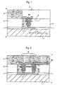
- FIG. 1 and 2 show that adjacent to the scoring frame R.
- the crackstop structure I prevents thin cracks from spreading in the inside of the semiconductor device, which may be when sawing along the scoring frame R can result while the Edgeseal structure II for sealing against moisture etc. serves.
- Both structures I and II consist of a lower connection layer C0 to a p-type diffusion region 2 a p-type silicon semiconductor substrate 1, which if necessary another p-type well below the diffusion area 2 may contain a lower metallization level M0, a middle connection layer C1 between the lower metallization level M0 and a middle one Metallization level M1 and an upper connection layer C2 between the middle metallization level M1 and an upper metallization level M2.
- the upper level of metallization M2 forms in the area of the Edge Seal structure II a ground or GND bus.
- the structures I and II are in a silicon dioxide layer 3 introduced within the structure I with a Photoimide and passivation layer 4 is provided.
- This Photoimide and passivation layer 4 covers the upper one Metallization M2 of structure II.
- Fig. 1 the area adjoining the scoring frame R forms the kerf. In this area and above the structure I the photoimide and passivation layer 4 is omitted.
- This recess 5 can if necessary also designed wider or provided several times become.
- the silicon dioxide layer 3 diluted, for which the process step to form the opening is used for the connection layer C2.
- this Process step are namely recesses 5 in the area of Kerfes generated, so that here the silicon dioxide layer 3 considerably is reduced in thickness, which is the subsequent Sawing the semiconductor wafer along the scoring frame R considerably facilitated.
- connection layers For the metallization levels and the connection layers For example, aluminum can be used. Possibly other metals can also be used.
- the p-type is in the illustrated embodiment Silicon semiconductor substrate 1 outside the p-type Diffusion zone 2 covered by a thin oxide layer 7.
- This oxide layer 7 can optionally also be omitted become.
- n-type semiconductor substrate instead of the p-type silicon semiconductor substrate also an n-type semiconductor substrate from another Semiconductor material can be used as silicon.
Landscapes
- Dicing (AREA)
Abstract
Description
Auch diese Maßnahme begünstigt ein einfacheres Zersägen des Halbleiterwafers in die einzelnen Halbleiterbausteine. Der Übergangsbereich kann dabei eine Breite von etwa 3 µm aufweisen.
- Fig. 1
- den Bereich eines Halbleiterbausteines in der Nähe eines Ritzrahmens R und
- Fig. 2
- einen an den Bereich der Fig. 1 längs einer Fläche AA anschließenden Bereich dieses Halbleiterbausteines.
- M0, M1, M2
- Metallisierungsebenen
- C0, C1, C2
- Verbindungsschichten zwischen Metallisierungsebenen
- R
- Ritzrahmen
- 1
- Halbleitersubstrat
- 2
- p-leitende Diffusionszone
- 3
- Siliziumdioxidschicht
- 4
- Photoemit- und Passivierungsschicht
- 5
- Ausnehmung
- 6
- Doppelpfeil für Übergangsbereich
- 7
- Oxidschicht
Claims (4)
- Anordnung zur Abtrennung eines Halbleiterbausteins aus einem Halbleiterwafer längs eines Ritzrahmens (R), bei der auf dem Halbleiterwafer eine Isolierschicht (3) vorgesehen ist, in der mehrere Metallisierungsebenen (M0, M1, M2) ausgebildet sind, von denen eine oberste Metallisierungsebene (M2) mit einer darunterliegenden Metallisierungsebene (M1) über eine Verbindungsschicht (C2) in einem Verbindungsloch elektrisch verbunden ist,
dadurch gekennzeichnet, daß im Übergangsbereich zwischen dem Halbleiterbaustein und dem Ritzrahmen (R) in die Isolierschicht (3) eine zusammen mit dem Verbindungsloch eingebrachte zusätzliche Ausnehmung (5) zur Verdünnung der Isolierschicht (3) vorgesehen ist. - Anordnung nach Anspruch 1,
dadurch gekennzeichnet, daß im Bereich der Ausnehmung (5) zwischen einem Halbleiterkörper (1) und dem Ritzrahmen (R) nur die Isolierschicht (3) auf dem Halbleiterkörper (1) vorgesehen ist. - Anordnung nach Anspruch 1 oder 2,
dadurch gekennzeichnet, daß der Übergangsbereich etwa 3 um breit ist. - Anordnung nach einem der Ansprüche 1 bis 3,
dadurch gekennzeichnet, daß zusammen mit der zusätzlichen Ausnehmung (5) im Übergangsbereich die Isolierschicht (3) durch weitere Ausnehmungen verdünnt ist.
Applications Claiming Priority (2)
| Application Number | Priority Date | Filing Date | Title |
|---|---|---|---|
| DE19961790 | 1999-12-21 | ||
| DE19961790A DE19961790C1 (de) | 1999-12-21 | 1999-12-21 | Anordnung zur Abtrennung eines Halbleiterbausteines aus einem Halbleiterwafer |
Publications (2)
| Publication Number | Publication Date |
|---|---|
| EP1111670A2 true EP1111670A2 (de) | 2001-06-27 |
| EP1111670A3 EP1111670A3 (de) | 2002-07-24 |
Family
ID=7933660
Family Applications (1)
| Application Number | Title | Priority Date | Filing Date |
|---|---|---|---|
| EP00126218A Withdrawn EP1111670A3 (de) | 1999-12-21 | 2000-11-30 | Anordnung zur Abtrennung eines Halbleiterbausteines aus einem Halbleiterwafer |
Country Status (7)
| Country | Link |
|---|---|
| US (1) | US6528392B2 (de) |
| EP (1) | EP1111670A3 (de) |
| JP (1) | JP2001203172A (de) |
| KR (1) | KR20020010439A (de) |
| CN (1) | CN1310472A (de) |
| DE (1) | DE19961790C1 (de) |
| TW (1) | TW480651B (de) |
Cited By (1)
| Publication number | Priority date | Publication date | Assignee | Title |
|---|---|---|---|---|
| US7380250B2 (en) | 2001-03-16 | 2008-05-27 | Microsoft Corporation | Method and system for interacting with devices having different capabilities |
Families Citing this family (16)
| Publication number | Priority date | Publication date | Assignee | Title |
|---|---|---|---|---|
| US6495918B1 (en) * | 2000-09-05 | 2002-12-17 | Infineon Technologies Ag | Chip crack stop design for semiconductor chips |
| US20050110151A1 (en) * | 2002-11-15 | 2005-05-26 | Itaru Tamura | Semiconductor device |
| TWI227936B (en) * | 2004-01-14 | 2005-02-11 | Taiwan Semiconductor Mfg | Sealed ring for IC protection |
| US7314811B2 (en) * | 2004-03-04 | 2008-01-01 | Chartered Semiconductor Manufacturing Ltd. | Method to make corner cross-grid structures in copper metallization |
| US7053453B2 (en) * | 2004-04-27 | 2006-05-30 | Taiwan Semiconductor Manufacturing Company, Ltd. | Substrate contact and method of forming the same |
| US7479447B2 (en) * | 2005-04-04 | 2009-01-20 | International Business Machines Corporation | Method of forming a crack stop void in a low-k dielectric layer between adjacent fuses |
| US8624346B2 (en) | 2005-10-11 | 2014-01-07 | Taiwan Semiconductor Manufacturing Company, Ltd. | Exclusion zone for stress-sensitive circuit design |
| US7952167B2 (en) | 2007-04-27 | 2011-05-31 | Taiwan Semiconductor Manufacturing Company, Ltd. | Scribe line layout design |
| US8125052B2 (en) * | 2007-05-14 | 2012-02-28 | Taiwan Semiconductor Manufacturing Co., Ltd. | Seal ring structure with improved cracking protection |
| US8643147B2 (en) * | 2007-11-01 | 2014-02-04 | Taiwan Semiconductor Manufacturing Company, Ltd. | Seal ring structure with improved cracking protection and reduced problems |
| US7704804B2 (en) | 2007-12-10 | 2010-04-27 | International Business Machines Corporation | Method of forming a crack stop laser fuse with fixed passivation layer coverage |
| US8334582B2 (en) * | 2008-06-26 | 2012-12-18 | Taiwan Semiconductor Manufacturing Company, Ltd. | Protective seal ring for preventing die-saw induced stress |
| US7906836B2 (en) | 2008-11-14 | 2011-03-15 | Taiwan Semiconductor Manufacturing Company, Ltd. | Heat spreader structures in scribe lines |
| US8368180B2 (en) * | 2009-02-18 | 2013-02-05 | Taiwan Semiconductor Manufacturing Company, Ltd. | Scribe line metal structure |
| US7892926B2 (en) | 2009-07-24 | 2011-02-22 | International Business Machines Corporation | Fuse link structures using film stress for programming and methods of manufacture |
| US8592941B2 (en) | 2010-07-19 | 2013-11-26 | International Business Machines Corporation | Fuse structure having crack stop void, method for forming and programming same, and design structure |
Family Cites Families (8)
| Publication number | Priority date | Publication date | Assignee | Title |
|---|---|---|---|---|
| US3798135A (en) * | 1972-05-03 | 1974-03-19 | Texas Instruments Inc | Anodic passivating processes for integrated circuits |
| US5136354A (en) * | 1989-04-13 | 1992-08-04 | Seiko Epson Corporation | Semiconductor device wafer with interlayer insulating film covering the scribe lines |
| JP2894165B2 (ja) * | 1993-07-24 | 1999-05-24 | ヤマハ株式会社 | 半導体装置 |
| US5686171A (en) * | 1993-12-30 | 1997-11-11 | Vlsi Technology, Inc. | Integrated circuit scribe line structures and methods for making same |
| US6022792A (en) * | 1996-03-13 | 2000-02-08 | Seiko Instruments, Inc. | Semiconductor dicing and assembling method |
| US5776826A (en) * | 1996-05-06 | 1998-07-07 | International Business Machines Corporation | Crack stop formation for high-productivity processes |
| KR0178134B1 (ko) * | 1996-10-01 | 1999-04-15 | 삼성전자주식회사 | 불연속 절연층 영역을 갖는 반도체 집적회로 소자 및 그 제조방법 |
| US5998282A (en) * | 1997-10-21 | 1999-12-07 | Lukaszek; Wieslaw A. | Method of reducing charging damage to integrated circuits in ion implant and plasma-based integrated circuit process equipment |
-
1999
- 1999-12-21 DE DE19961790A patent/DE19961790C1/de not_active Expired - Lifetime
-
2000
- 2000-11-30 EP EP00126218A patent/EP1111670A3/de not_active Withdrawn
- 2000-12-18 JP JP2000383537A patent/JP2001203172A/ja not_active Withdrawn
- 2000-12-20 TW TW089127354A patent/TW480651B/zh not_active IP Right Cessation
- 2000-12-21 CN CN00136488A patent/CN1310472A/zh active Pending
- 2000-12-21 US US09/745,541 patent/US6528392B2/en not_active Expired - Lifetime
- 2000-12-21 KR KR1020000079685A patent/KR20020010439A/ko not_active Withdrawn
Cited By (1)
| Publication number | Priority date | Publication date | Assignee | Title |
|---|---|---|---|---|
| US7380250B2 (en) | 2001-03-16 | 2008-05-27 | Microsoft Corporation | Method and system for interacting with devices having different capabilities |
Also Published As
| Publication number | Publication date |
|---|---|
| TW480651B (en) | 2002-03-21 |
| US6528392B2 (en) | 2003-03-04 |
| JP2001203172A (ja) | 2001-07-27 |
| US20010005617A1 (en) | 2001-06-28 |
| EP1111670A3 (de) | 2002-07-24 |
| DE19961790C1 (de) | 2001-05-10 |
| KR20020010439A (ko) | 2002-02-04 |
| CN1310472A (zh) | 2001-08-29 |
Similar Documents
| Publication | Publication Date | Title |
|---|---|---|
| EP1111670A2 (de) | Anordnung zur Abtrennung eines Halbleiterbausteines aus einem Halbleiterwafer | |
| DE60126960T2 (de) | Verbesserter rissunterbrecher für halbleiterchips | |
| DE10125407B4 (de) | Verbesserte elektronische Sicherungen durch die lokale Verschlechterung der schmelzbaren Verbindung | |
| DE102009044597B4 (de) | Halbleiter-Bauelement und Verfahren zur Herstellung desselben | |
| DE102006043484B4 (de) | Fuse-Struktur und Verfahren zum Herstellen derselben | |
| DE102014204600B4 (de) | Wafer, integrierter schaltungschip und verfahren zur herstellung eines integrierten schaltungschips | |
| DE102014102087B4 (de) | Kontaktflecke über prozesssteuerungs-/überwachungs-strukturen in einem halbleiterchip | |
| DE102011054153A1 (de) | Rissstoppbarriere und Verfahren zu deren Herstellung | |
| DE4020195A1 (de) | Halbleiterchip und verfahren zu seiner herstellung | |
| DE19619921A1 (de) | Verfahren zum Herstellen einer Halbleitervorrichtung | |
| DE102012008068A1 (de) | Optionen für mehrere Ebenen eines Leistungs-MOSFET | |
| DE69714134T2 (de) | Rissunterbrecher auf Chips mit integrierter Schaltung | |
| DE3617141C2 (de) | ||
| DE112005001578T5 (de) | Bond-Pad-Struktur zur Kupfer-Metallisierung mit verbesserter Zuverlässigkeit, und Verfahren zum Herstellen dieser Struktur | |
| DE4239457C2 (de) | Halbleiterwaferstruktur und Herstellungsverfahren dafür | |
| DE19829472A1 (de) | Halbleiterbauelement und Verfahren zu dessen Herstellung | |
| DE102019124181A1 (de) | Vereinzelungsverfahren für gestapelte halbleiterbauelemente | |
| EP1198836B1 (de) | Fuse für halbleiteranordnung | |
| DE10306949A1 (de) | Halbleitereinrichtung | |
| DE102012007954A1 (de) | Doppelschichtmetall- (DLM) Leistungs-MOSFET | |
| DE69321966T2 (de) | Leistungs-Halbleiterbauelement | |
| DE3930622C2 (de) | Statischer RAM | |
| DE112004003008T5 (de) | Halbleiterbauelement und Verfahren zur Herstellung desselben | |
| DE19926499C2 (de) | Anordnung von Fuses bei Halbleiterstrukturen mit Cu-Metallisierung | |
| DE69723044T2 (de) | Verfahren zur Herstellung von einer Randstruktur um ein integriertes elektronisches Bauelement zu versiegeln, sowie ein entsprechendes Bauelement |
Legal Events
| Date | Code | Title | Description |
|---|---|---|---|
| PUAI | Public reference made under article 153(3) epc to a published international application that has entered the european phase |
Free format text: ORIGINAL CODE: 0009012 |
|
| AK | Designated contracting states |
Kind code of ref document: A2 Designated state(s): AT BE CH CY DE DK ES FI FR GB GR IE IT LI LU MC NL PT SE TR |
|
| AX | Request for extension of the european patent |
Free format text: AL;LT;LV;MK;RO;SI |
|
| PUAL | Search report despatched |
Free format text: ORIGINAL CODE: 0009013 |
|
| AK | Designated contracting states |
Kind code of ref document: A3 Designated state(s): AT BE CH CY DE DK ES FI FR GB GR IE IT LI LU MC NL PT SE TR |
|
| AX | Request for extension of the european patent |
Free format text: AL;LT;LV;MK;RO;SI |
|
| 17P | Request for examination filed |
Effective date: 20030115 |
|
| 17Q | First examination report despatched |
Effective date: 20030227 |
|
| AKX | Designation fees paid |
Designated state(s): DE GB |
|
| STAA | Information on the status of an ep patent application or granted ep patent |
Free format text: STATUS: THE APPLICATION IS DEEMED TO BE WITHDRAWN |
|
| 18D | Application deemed to be withdrawn |
Effective date: 20041007 |