EP1107305A2 - Methode zur Montage eines Halbleitervorrichtung - Google Patents
Methode zur Montage eines Halbleitervorrichtung Download PDFInfo
- Publication number
- EP1107305A2 EP1107305A2 EP00127089A EP00127089A EP1107305A2 EP 1107305 A2 EP1107305 A2 EP 1107305A2 EP 00127089 A EP00127089 A EP 00127089A EP 00127089 A EP00127089 A EP 00127089A EP 1107305 A2 EP1107305 A2 EP 1107305A2
- Authority
- EP
- European Patent Office
- Prior art keywords
- metallic
- semiconductor device
- ultra
- fine particle
- fine particles
- Prior art date
- Legal status (The legal status is an assumption and is not a legal conclusion. Google has not performed a legal analysis and makes no representation as to the accuracy of the status listed.)
- Withdrawn
Links
Images



Classifications
-
- H—ELECTRICITY
- H05—ELECTRIC TECHNIQUES NOT OTHERWISE PROVIDED FOR
- H05K—PRINTED CIRCUITS; CASINGS OR CONSTRUCTIONAL DETAILS OF ELECTRIC APPARATUS; MANUFACTURE OF ASSEMBLAGES OF ELECTRICAL COMPONENTS
- H05K3/00—Apparatus or processes for manufacturing printed circuits
- H05K3/30—Assembling printed circuits with electric components, e.g. with resistors
- H05K3/32—Assembling printed circuits with electric components, e.g. with resistors electrically connecting electric components or wires to printed circuits
- H05K3/34—Assembling printed circuits with electric components, e.g. with resistors electrically connecting electric components or wires to printed circuits by soldering
- H05K3/341—Surface mounted components
- H05K3/3431—Leadless components
- H05K3/3436—Leadless components having an array of bottom contacts, e.g. pad grid array or ball grid array components
-
- H—ELECTRICITY
- H10—SEMICONDUCTOR DEVICES; ELECTRIC SOLID-STATE DEVICES NOT OTHERWISE PROVIDED FOR
- H10W—GENERIC PACKAGES, INTERCONNECTIONS, CONNECTORS OR OTHER CONSTRUCTIONAL DETAILS OF DEVICES COVERED BY CLASS H10
- H10W72/00—Interconnections or connectors in packages
-
- H—ELECTRICITY
- H10—SEMICONDUCTOR DEVICES; ELECTRIC SOLID-STATE DEVICES NOT OTHERWISE PROVIDED FOR
- H10W—GENERIC PACKAGES, INTERCONNECTIONS, CONNECTORS OR OTHER CONSTRUCTIONAL DETAILS OF DEVICES COVERED BY CLASS H10
- H10W72/00—Interconnections or connectors in packages
- H10W72/01—Manufacture or treatment
- H10W72/011—Apparatus therefor
- H10W72/0112—Apparatus for manufacturing bump connectors
-
- H—ELECTRICITY
- H10—SEMICONDUCTOR DEVICES; ELECTRIC SOLID-STATE DEVICES NOT OTHERWISE PROVIDED FOR
- H10W—GENERIC PACKAGES, INTERCONNECTIONS, CONNECTORS OR OTHER CONSTRUCTIONAL DETAILS OF DEVICES COVERED BY CLASS H10
- H10W72/00—Interconnections or connectors in packages
- H10W72/01—Manufacture or treatment
- H10W72/019—Manufacture or treatment of bond pads
-
- H—ELECTRICITY
- H10—SEMICONDUCTOR DEVICES; ELECTRIC SOLID-STATE DEVICES NOT OTHERWISE PROVIDED FOR
- H10W—GENERIC PACKAGES, INTERCONNECTIONS, CONNECTORS OR OTHER CONSTRUCTIONAL DETAILS OF DEVICES COVERED BY CLASS H10
- H10W72/00—Interconnections or connectors in packages
- H10W72/071—Connecting or disconnecting
- H10W72/0711—Apparatus therefor
-
- H—ELECTRICITY
- H05—ELECTRIC TECHNIQUES NOT OTHERWISE PROVIDED FOR
- H05K—PRINTED CIRCUITS; CASINGS OR CONSTRUCTIONAL DETAILS OF ELECTRIC APPARATUS; MANUFACTURE OF ASSEMBLAGES OF ELECTRICAL COMPONENTS
- H05K1/00—Printed circuits
- H05K1/02—Details
- H05K1/09—Use of materials for the conductive, e.g. metallic pattern
- H05K1/092—Dispersed materials, e.g. conductive pastes or inks
- H05K1/095—Dispersed materials, e.g. conductive pastes or inks for polymer thick films, i.e. having a permanent organic polymeric binder
-
- H—ELECTRICITY
- H05—ELECTRIC TECHNIQUES NOT OTHERWISE PROVIDED FOR
- H05K—PRINTED CIRCUITS; CASINGS OR CONSTRUCTIONAL DETAILS OF ELECTRIC APPARATUS; MANUFACTURE OF ASSEMBLAGES OF ELECTRICAL COMPONENTS
- H05K2201/00—Indexing scheme relating to printed circuits covered by H05K1/00
- H05K2201/02—Fillers; Particles; Fibers; Reinforcement materials
- H05K2201/0203—Fillers and particles
- H05K2201/0242—Shape of an individual particle
- H05K2201/0257—Nanoparticles
-
- H—ELECTRICITY
- H05—ELECTRIC TECHNIQUES NOT OTHERWISE PROVIDED FOR
- H05K—PRINTED CIRCUITS; CASINGS OR CONSTRUCTIONAL DETAILS OF ELECTRIC APPARATUS; MANUFACTURE OF ASSEMBLAGES OF ELECTRICAL COMPONENTS
- H05K2201/00—Indexing scheme relating to printed circuits covered by H05K1/00
- H05K2201/10—Details of components or other objects attached to or integrated in a printed circuit board
- H05K2201/10613—Details of electrical connections of non-printed components, e.g. special leads
- H05K2201/10621—Components characterised by their electrical contacts
- H05K2201/10674—Flip chip
-
- H—ELECTRICITY
- H10—SEMICONDUCTOR DEVICES; ELECTRIC SOLID-STATE DEVICES NOT OTHERWISE PROVIDED FOR
- H10W—GENERIC PACKAGES, INTERCONNECTIONS, CONNECTORS OR OTHER CONSTRUCTIONAL DETAILS OF DEVICES COVERED BY CLASS H10
- H10W72/00—Interconnections or connectors in packages
- H10W72/01—Manufacture or treatment
- H10W72/012—Manufacture or treatment of bump connectors, dummy bumps or thermal bumps
- H10W72/01215—Manufacture or treatment of bump connectors, dummy bumps or thermal bumps forming coatings
-
- H—ELECTRICITY
- H10—SEMICONDUCTOR DEVICES; ELECTRIC SOLID-STATE DEVICES NOT OTHERWISE PROVIDED FOR
- H10W—GENERIC PACKAGES, INTERCONNECTIONS, CONNECTORS OR OTHER CONSTRUCTIONAL DETAILS OF DEVICES COVERED BY CLASS H10
- H10W72/00—Interconnections or connectors in packages
- H10W72/01—Manufacture or treatment
- H10W72/012—Manufacture or treatment of bump connectors, dummy bumps or thermal bumps
- H10W72/01261—Chemical or physical modification, e.g. by sintering or anodisation
-
- H—ELECTRICITY
- H10—SEMICONDUCTOR DEVICES; ELECTRIC SOLID-STATE DEVICES NOT OTHERWISE PROVIDED FOR
- H10W—GENERIC PACKAGES, INTERCONNECTIONS, CONNECTORS OR OTHER CONSTRUCTIONAL DETAILS OF DEVICES COVERED BY CLASS H10
- H10W72/00—Interconnections or connectors in packages
- H10W72/071—Connecting or disconnecting
- H10W72/072—Connecting or disconnecting of bump connectors
-
- H—ELECTRICITY
- H10—SEMICONDUCTOR DEVICES; ELECTRIC SOLID-STATE DEVICES NOT OTHERWISE PROVIDED FOR
- H10W—GENERIC PACKAGES, INTERCONNECTIONS, CONNECTORS OR OTHER CONSTRUCTIONAL DETAILS OF DEVICES COVERED BY CLASS H10
- H10W72/00—Interconnections or connectors in packages
- H10W72/071—Connecting or disconnecting
- H10W72/073—Connecting or disconnecting of die-attach connectors
- H10W72/07331—Connecting techniques
- H10W72/07336—Soldering or alloying
-
- H—ELECTRICITY
- H10—SEMICONDUCTOR DEVICES; ELECTRIC SOLID-STATE DEVICES NOT OTHERWISE PROVIDED FOR
- H10W—GENERIC PACKAGES, INTERCONNECTIONS, CONNECTORS OR OTHER CONSTRUCTIONAL DETAILS OF DEVICES COVERED BY CLASS H10
- H10W72/00—Interconnections or connectors in packages
- H10W72/20—Bump connectors, e.g. solder bumps or copper pillars; Dummy bumps; Thermal bumps
- H10W72/241—Dispositions, e.g. layouts
-
- H—ELECTRICITY
- H10—SEMICONDUCTOR DEVICES; ELECTRIC SOLID-STATE DEVICES NOT OTHERWISE PROVIDED FOR
- H10W—GENERIC PACKAGES, INTERCONNECTIONS, CONNECTORS OR OTHER CONSTRUCTIONAL DETAILS OF DEVICES COVERED BY CLASS H10
- H10W72/00—Interconnections or connectors in packages
- H10W72/20—Bump connectors, e.g. solder bumps or copper pillars; Dummy bumps; Thermal bumps
- H10W72/251—Materials
-
- H—ELECTRICITY
- H10—SEMICONDUCTOR DEVICES; ELECTRIC SOLID-STATE DEVICES NOT OTHERWISE PROVIDED FOR
- H10W—GENERIC PACKAGES, INTERCONNECTIONS, CONNECTORS OR OTHER CONSTRUCTIONAL DETAILS OF DEVICES COVERED BY CLASS H10
- H10W72/00—Interconnections or connectors in packages
- H10W72/20—Bump connectors, e.g. solder bumps or copper pillars; Dummy bumps; Thermal bumps
- H10W72/251—Materials
- H10W72/252—Materials comprising solid metals or solid metalloids, e.g. PbSn, Ag or Cu
-
- H—ELECTRICITY
- H10—SEMICONDUCTOR DEVICES; ELECTRIC SOLID-STATE DEVICES NOT OTHERWISE PROVIDED FOR
- H10W—GENERIC PACKAGES, INTERCONNECTIONS, CONNECTORS OR OTHER CONSTRUCTIONAL DETAILS OF DEVICES COVERED BY CLASS H10
- H10W72/00—Interconnections or connectors in packages
- H10W72/30—Die-attach connectors
- H10W72/321—Structures or relative sizes of die-attach connectors
- H10W72/325—Die-attach connectors having a filler embedded in a matrix
-
- H—ELECTRICITY
- H10—SEMICONDUCTOR DEVICES; ELECTRIC SOLID-STATE DEVICES NOT OTHERWISE PROVIDED FOR
- H10W—GENERIC PACKAGES, INTERCONNECTIONS, CONNECTORS OR OTHER CONSTRUCTIONAL DETAILS OF DEVICES COVERED BY CLASS H10
- H10W72/00—Interconnections or connectors in packages
- H10W72/30—Die-attach connectors
- H10W72/351—Materials of die-attach connectors
- H10W72/352—Materials of die-attach connectors comprising metals or metalloids, e.g. solders
-
- H—ELECTRICITY
- H10—SEMICONDUCTOR DEVICES; ELECTRIC SOLID-STATE DEVICES NOT OTHERWISE PROVIDED FOR
- H10W—GENERIC PACKAGES, INTERCONNECTIONS, CONNECTORS OR OTHER CONSTRUCTIONAL DETAILS OF DEVICES COVERED BY CLASS H10
- H10W72/00—Interconnections or connectors in packages
- H10W72/90—Bond pads, in general
- H10W72/921—Structures or relative sizes of bond pads
- H10W72/923—Bond pads having multiple stacked layers
-
- H—ELECTRICITY
- H10—SEMICONDUCTOR DEVICES; ELECTRIC SOLID-STATE DEVICES NOT OTHERWISE PROVIDED FOR
- H10W—GENERIC PACKAGES, INTERCONNECTIONS, CONNECTORS OR OTHER CONSTRUCTIONAL DETAILS OF DEVICES COVERED BY CLASS H10
- H10W72/00—Interconnections or connectors in packages
- H10W72/90—Bond pads, in general
- H10W72/941—Dispositions of bond pads
- H10W72/9415—Dispositions of bond pads relative to the surface, e.g. recessed, protruding
-
- H—ELECTRICITY
- H10—SEMICONDUCTOR DEVICES; ELECTRIC SOLID-STATE DEVICES NOT OTHERWISE PROVIDED FOR
- H10W—GENERIC PACKAGES, INTERCONNECTIONS, CONNECTORS OR OTHER CONSTRUCTIONAL DETAILS OF DEVICES COVERED BY CLASS H10
- H10W90/00—Package configurations
- H10W90/701—Package configurations characterised by the relative positions of pads or connectors relative to package parts
- H10W90/721—Package configurations characterised by the relative positions of pads or connectors relative to package parts of bump connectors
- H10W90/724—Package configurations characterised by the relative positions of pads or connectors relative to package parts of bump connectors between a chip and a stacked insulating package substrate, interposer or RDL
-
- Y—GENERAL TAGGING OF NEW TECHNOLOGICAL DEVELOPMENTS; GENERAL TAGGING OF CROSS-SECTIONAL TECHNOLOGIES SPANNING OVER SEVERAL SECTIONS OF THE IPC; TECHNICAL SUBJECTS COVERED BY FORMER USPC CROSS-REFERENCE ART COLLECTIONS [XRACs] AND DIGESTS
- Y02—TECHNOLOGIES OR APPLICATIONS FOR MITIGATION OR ADAPTATION AGAINST CLIMATE CHANGE
- Y02P—CLIMATE CHANGE MITIGATION TECHNOLOGIES IN THE PRODUCTION OR PROCESSING OF GOODS
- Y02P70/00—Climate change mitigation technologies in the production process for final industrial or consumer products
- Y02P70/50—Manufacturing or production processes characterised by the final manufactured product
-
- Y—GENERAL TAGGING OF NEW TECHNOLOGICAL DEVELOPMENTS; GENERAL TAGGING OF CROSS-SECTIONAL TECHNOLOGIES SPANNING OVER SEVERAL SECTIONS OF THE IPC; TECHNICAL SUBJECTS COVERED BY FORMER USPC CROSS-REFERENCE ART COLLECTIONS [XRACs] AND DIGESTS
- Y10—TECHNICAL SUBJECTS COVERED BY FORMER USPC
- Y10T—TECHNICAL SUBJECTS COVERED BY FORMER US CLASSIFICATION
- Y10T29/00—Metal working
- Y10T29/49—Method of mechanical manufacture
- Y10T29/49002—Electrical device making
- Y10T29/49117—Conductor or circuit manufacturing
- Y10T29/49124—On flat or curved insulated base, e.g., printed circuit, etc.
- Y10T29/4913—Assembling to base an electrical component, e.g., capacitor, etc.
-
- Y—GENERAL TAGGING OF NEW TECHNOLOGICAL DEVELOPMENTS; GENERAL TAGGING OF CROSS-SECTIONAL TECHNOLOGIES SPANNING OVER SEVERAL SECTIONS OF THE IPC; TECHNICAL SUBJECTS COVERED BY FORMER USPC CROSS-REFERENCE ART COLLECTIONS [XRACs] AND DIGESTS
- Y10—TECHNICAL SUBJECTS COVERED BY FORMER USPC
- Y10T—TECHNICAL SUBJECTS COVERED BY FORMER US CLASSIFICATION
- Y10T29/00—Metal working
- Y10T29/49—Method of mechanical manufacture
- Y10T29/49002—Electrical device making
- Y10T29/49117—Conductor or circuit manufacturing
- Y10T29/49124—On flat or curved insulated base, e.g., printed circuit, etc.
- Y10T29/4913—Assembling to base an electrical component, e.g., capacitor, etc.
- Y10T29/49144—Assembling to base an electrical component, e.g., capacitor, etc. by metal fusion
-
- Y—GENERAL TAGGING OF NEW TECHNOLOGICAL DEVELOPMENTS; GENERAL TAGGING OF CROSS-SECTIONAL TECHNOLOGIES SPANNING OVER SEVERAL SECTIONS OF THE IPC; TECHNICAL SUBJECTS COVERED BY FORMER USPC CROSS-REFERENCE ART COLLECTIONS [XRACs] AND DIGESTS
- Y10—TECHNICAL SUBJECTS COVERED BY FORMER USPC
- Y10T—TECHNICAL SUBJECTS COVERED BY FORMER US CLASSIFICATION
- Y10T29/00—Metal working
- Y10T29/53—Means to assemble or disassemble
- Y10T29/5313—Means to assemble electrical device
- Y10T29/53174—Means to fasten electrical component to wiring board, base, or substrate
- Y10T29/53178—Chip component
Definitions
- This invention relates to a method for electrically connecting electrodes of a semiconductor device (chip, pellet or die) to terminal electrodes on a circuit board. More specifically, the invention relates to a method for mounting a semiconductor device by face down bonding using metallic paste for connection, or a method for mounting a semiconductor device which involves the use of solder bumps for electrical connection of electrodes; a mounted structure of a semiconductor device produced by any of these methods; and a mounting system for the methods and the mounted structure.
- Soldering has been generally used for electrical connection of connecting electrodes of an electronic device to circuit pattern terminals on a circuit board.
- a small package such as an IC flat package, has come into use, and the number of connecting terminals has increased.
- a so-called pitch between adjacent connecting terminals has gradually narrowed, and it has become gradually difficult for a conventional soldering technique to provide electrical connections stably in such a narrow pitch.
- the face down bonding method comprises forming solder bumps beforehand on electrode pads of the semiconductor device, placing the solder bumps so as to downwardly face terminal electrodes on the circuit board, and heating the solder bumps at a high temperature to fusion bond the electrode of semiconductor device to the terminal electrode of circuit board.
- the solder bumps are generally formed on three metallic thin films (under bump metals) comprising, for example, Cr (chromium), Cu (copper) and Au (gold), by soldering, plating or vapor deposition using a resist pattern.
- This mounting method imparts high mechanical strength after connection, and is capable of electrically connecting the plural electrodes of the semiconductor device to the terminal electrodes of the circuit board at a time. Thus, it has been considered an effective method for mounting a semiconductor device.
- the three metallic thin films comprising, for example, Cr (chromium), Cu (copper) and Au (gold) need to be formed prior to the formation of the solder bumps. Formation of these thin films has required not only considerably extensive equipment, but also mask management and vacuum management, thus leading to increase in the cost and working time. According to the conventional method of mounting a semiconductor device using solder bumps, moreover, the solder spreads during heat fusion, and the adjacent solder bumps (electrodes) may form short-circuit. Thus, this method may fail to be applied to micro-fabricated products.
- the metallic ultra-fine particles used in this method are considered to be ultra-fine particles of a metal alone which were prepared, for example, by the following method: A metal is evaporated in a vacuum in the presence of a small amount of gas to coagulate ultra-fine particles consisting only of metal from a vapor phase, thereby obtaining ultra-fine metallic particles.
- Such metallic ultra-fine particles may be problematical in stability, physical properties, and cost.
- An object of the present invention is to provide a method for mounting a semiconductor device, the method enabling the solder bump method to be conveniently performed, and being capable of realizing a highly stable, low-cost, high reliability electrical connection, and also provide a mounted structure by this method.
- Another object of the invention is to provide a method for mounting a semiconductor device, the method being capable of realizing a highly stable, low-cost, high reliability electrical connection, which has no risk of short-circuiting adjacent electrodes of even a narrow pitch; and a mounted structure of the semiconductor device produced by this method.
- the method, the structure and the system are characterized by using one of, or a combination of, the following two bump technologies:
- an aspect of the present invention is a method for mounting a semiconductor device, comprising: preparing a metallic ultra-fine particle paste by dispersing compound metallic ultra-fine particles in a solvent, the compound metallic ultra-fine particles each comprising a core portion consisting substantially of a metallic component and a coating layer chemically bound to the core portion and comprising an organic substance; forming ultra-fine particle electrodes by attaching the metallic fine particle paste onto electrodes of the semiconductor device, followed by low temperature heat process; forming solder bumps on the ultra-fine particle electrodes; and connecting the solder bumps to terminal electrodes of a circuit board by heat fusing thereof.
- the metallic fine particle paste is adhered onto the electrodes of the semiconductor device, and subjected to low temperature heat process.
- the ultra-fine particle electrodes which serve as under bump metals for solder bumps, can be formed easily and promptly without using extensive equipment.
- Another aspect of the present invention is a method for mounting a semiconductor device, comprising: preparing a metallic fine particle paste by dispersing compound metallic ultra-fine particles in a solvent, the compound metallic ultra-fine particles each comprising a core portion consisting substantially of a metallic component, and a coating layer chemically bound to the core portion and comprising an organic substance; forming metallic fine particle paste balls consisting mainly of the compound metallic ultra-fine particles by attaching the metallic fine particle paste onto terminal electrodes of a circuit board; connecting electrodes of the semiconductor device onto the metallic fine particle paste balls by the face down bonding method; and electrically connecting electrodes of the semiconductor device and the circuit board by low temperature heat process.
- the compound metallic ultra-fine particles can be prepared by a chemical process in a liquid phase. Thus, they can be mass produced in an ordinary atmospheric state, for a low cost, with the use of a simple apparatus without the need to use an extensive apparatus. Furthermore, the compound metallic ultra-fine particles have an organic substance as the coating layer. Thus, when in the solvent, these particles are minimally aggregatable, stable and easy to handle. Consequently, the metallic fine particle paste having the compound metallic ultra-fine particles uniformly dispersed therein can be prepared, and process control for the metallic fine particle paste is easy. Moreover, the particle diameters are uniform, so that all the compound metallic ultra-fine particles are fused and bound together at a constant temperature during low temperature heat treatment.
- the core portion is a positively charged, metallic ultra-fine particle of Ag, Au or Pb with an average particle diameter of 1 to 10 nm
- the coating layer is an organic anion having 5 or more carbon atoms.
- the low temperature heat process is performed in a temperature range of 200 to 300°C.
- the temperature is not lower than the temperature at which the coating layer is released from the core portion and core portions are fused and bound together.
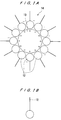
- a compound metallic ultra-fine particle 14 comprising a core portion 10 and a coating layer 12 is prepared.
- the core portion 10 consists substantially of a metallic component, and the coating layer 12 comprises an organic substance.
- the compound metallic ultra-fine particle 14 has its core covered with the coating layer 12 comprising the organic substance.
- the compound metallic ultra-fine particle 14 is stable, and has a low tendency to aggregate in a solvent.
- the compound metallic ultra-fine particle 14 is composed of the organic substance and the metallic component, which is derived from a metal salt as a starting material, e.g., a carbonate, a formate or an acetate.
- the center portion of the compound metallic ultra-fine particle 14 comprises the metallic component, which is surrounded with an ionic organic substance.
- the organic substance and the metallic component are combined integrally, with part or all of them being chemically bonded together.
- the compound metallic ultra-fine particle 14 has high stability, and is also stable even at a higher metal concentration.
- the average particle diameter of the core portion 10 of the compound metallic ultra-fine particle 14 is 1 to 10 nm.
- the compound metallic ultra-fine particle 14 can be produced, for example, by heating a metal salt, such as a carbonate, formate or acetate, in a nonaqueous solvent and in the presence of an ionic organic substance, at a temperature not lower than the decomposition reduction temperature of the metal salt, but lower than the decomposition temperature of the ionic organic substance.
- a metal salt such as a carbonate, formate or acetate
- an ionic organic substance is suitably used.
- the ionic organic substance a fatty acid, an alkylbenzenesulfonic acid, or an alkylsulfonic acid, each having 5 or more carbon atoms, is used.
- the heating temperature is not lower than the decomposition reduction temperature of the metal salt such as a carbonate, formate or acetate, but lower than the decomposition temperature of the ionic organic substance.
- the temperature at which its decomposition begins is 200°C.
- silver acetate may be held at a temperature of higher than 200°C, and at a temperature at which the ionic organic substance is not decomposed.
- heating atmosphere is preferably inert gas atmosphere. By selecting a nonaqueous solvent, however, heating can be performed even in the air.
- various alcohols can be added, whereby the reaction can be promoted.
- the alcohols are not restricted, as long as the above effect is obtained.
- Their examples are lauryl alcohol, glycerin, and ethylene glycol.
- the amount of the alcohol added can be determined, as desired, depending on the type of the alcohol used. Normally, the alcohol may be added in an amount of about 5 to 20 parts by weight, preferably 5 to 10 parts by weight, with respect to 100 parts by weight of the metal salt.
- purification is performed by a publicly known purification method.
- the purification method may, for example, be centrifugation, membrane purification, or solvent extraction.
- oleic acid is used as an organic anionic substance
- silver acetate is used as a metal source.
- These materials are placed in a naphthenic high boiling solvent having a distillation point of 250°C.
- the mixture is heated for 3 hours at 240°C, and acetone is further added for precipitation and purification.
- compound metallic ultra-fine particles can be prepared.
- the compound metallic ultra-fine particles comprise clustered, positively charged Ag metallic ultra-fine particles (core metal) with an average particle diameter of about 10 nm, and organic anions (coating layer) coating the circumference of the metallic particles.
- the resulting compound metallic ultra-fine particles 14 are dispersed in a predetermined solvent such as toluene, and if desired, a resin or an additive is added to prepare a metallic paste.
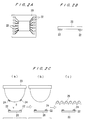
- FIGS. 2A to FIG. 6 A first embodiment of the present invention will be described with reference to FIGS. 2A to FIG. 6.
- Such a metallic paste 44 is almost transparent and the physical properties of the metallic paste 24 such as surface tension and viscosity, can be adjusted by selecting the type of the solvent, the concentration of the compound metallic ultra-fine particles, and the temperature, as desired.
- the metallic paste 24 is subjected to low temperature heat process as shown in FIG. 2C(c), for example, at 200 to 300°C to form ultra-fine particle electrodes 26 comprising the core portions (metal) 10 of the compound metallic ultra-fine particles 14.
- the solvent, such as toluene, contained in the metallic paste 24 is evaporated.
- the compound metallic ultra-fine particles 24 as the main component of the metallic paste 24 are heated at a temperature not lower than the temperature at which the coating layer (organic substance) 12 (see FIGS. 1A and 1B) is released from the core portion 10 or the coating layer 12 itself is decomposed.
- the coating layer 12 is released from the core portion 10, or the coating layer 12 is decomposed to vanish.
- the core portions 10 are fused and bound together to form ultra-fine particle electrodes 26.
- the ultra-fine particle electrodes 26 serve as under bump metals for solder bumps 32.
- the ultra-fine particle electrode 26 can be formed easily and promptly without using extensive equipments such as expensive photolithography equipments or chemical vapor deposition equipments.
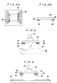
- the solder bumps 32 are formed on the ultra-fine particle electrodes 26, for example, by dipping the ultra-fine particle electrodes 26 in a molten solder bath 30 and lifting them, as shown by virtual lines in FIG. 4. The dipping is carried out by using solder bump forming device 27 including the molten solder bath 30.
- the solder bumps 32 may be formed on the ultra-fine particle electrodes 26 by printing a solder paste.
- the solder bumps 32 provided on the semiconductor device 20 are connected to predetermined positions on terminal electrodes 42 of a circuit board 40 by the flip chip bonding method in which the solder bumps 32 of the semiconductor device 20 and the terminal electrodes 42 of the circuit board 40 are aligned, with the semiconductor device 20 upside down in a face down manner.
- face down bonding is carried out by using bonding device 29.
- the resulting assembly is passed through, for example, a heat treatment furnace for reflow of the solder constituting the solder bumps 32 to perform heat fusing with the terminal electrodes 42 of the circuit board 40.
- a heat treatment furnace for reflow of the solder constituting the solder bumps 32 to perform heat fusing with the terminal electrodes 42 of the circuit board 40.
- the plurality of solder bumps 32 and the terminal electrodes 42 of the circuit board 40 can be electrically connected at a time.
- the solder bump method can be performed conveniently, and a highly stable, low-cost, high reliability electrical connection can be realized to mount a semiconductor device on a circuit board.
- mounting steps are preformed by a mounting system which uses printing device 23 for printing metallic paste as shown in FIG. 2C, lamp furnace 25 for forming under bump layer as shown in FIG. 2C, bonding device 29 for bonding semiconductor device 20 onto circuit board 40 as shown in FIG. 5, and furnace for heat treatment to form solder connections between solder bumps 32 and terminal electrodes 42 on the circuit board 40.
- the under metal layer 26 comprised by metallic ultra-fine particles fused and bound together is formed by printing device 23 and lamp furnace 25.
- the solder bump 32 is formed by solder bump forming device 27. Electrical connection between the bump and the terminal electrode is securely formed by the heat treatment furnace 31.
- the interposed devices 35 are utilities for stocking the products or cooling the products, etc.
- the mounting system is also equipped with load/unload device 37 and handling robot 39.
- Each device of the mounting system is controlled independently by a computer. However, informations of process steps are exchanged each other, and process informations are feed-back controlled. Thus optimum process control of the mounting system can be performed.
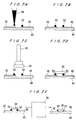
- FIGS. 7A, 7B, 7C, 7D and 7E Next, a second embodiment of the present invention will be described with reference to FIGS. 7A, 7B, 7C, 7D and 7E.
- the step of preparing a compound metallic ultra-fine particle 14 comprising a core portion 10 consisting substantially of a metallic component, and a coating layer 12 comprising an organic substance, as shown in FIGS. 1A and 1B, is the same as early described.
- the resulting compound metallic ultra-fine particles 14 are dispersed in a predetermined solvent such as toluene, and if desired, a metal having high electrical conductivity and measuring about 0.1 to 1 ⁇ m, such as Ag, Au, Pd or Al, and a resin or an additive is added to prepare a metallic paste.
- the metallic paste is dripped onto predetermined positions of terminal electrodes 42 of a circuit board 40 by using dripping device 54.
- the dripped paste forms about 2 ⁇ m high metallic paste balls 52 consisting mainly of the compound metallic ultra-fine particles 14 as shown in FIG. 7B.
- Such a metallic paste is almost transparent because when in a solvent in which the compound metallic ultra-fine particles 14 have been mixed and stirred, the compound metallic ultra-fine particles 14 are very fine.
- the physical properties of the metallic paste such as surface tension and viscosity, can be adjusted by selecting the type of the solvent, the concentration of the compound metallic ultra-fine particles, and the temperature, as desired.
- electrode pads provided on a semiconductor device 20 are connected onto the metallic paste balls 52, by the flip chip bonding device 56 in which the electrode pads of the semiconductor device 20 and the metallic paste balls 52 are aligned, with the semiconductor device 20 upside down in a face down manner. If desired, leveling is carried out with the use of the weight onto the semiconductor device 30. Then the semiconductor device 20 is bonded onto circuit board 40 via metallic paste balls 52 as shown in FIG. 7D.
- low temperature firing heat treatment
- a furnace 58 to form a conductor connector portion 53 which electrically connects the semiconductor device 20 and the circuit board 40.
- the solvent such as toluene
- the compound metallic ultra-fine particles 14 as the main component of the metallic paste balls 52 are heated at a temperature not lower than the temperature at which the coating layer (organic substance) 12 (see FIGS. 1A and 1B) is released from the core portion 10 or the coating layer 12 itself is decomposed.
- the coating layer 12 is released from the core portion 10, or the coating layer 12 is decomposed to vanish.
- the core portions 10 are fused and bound together to form metal conductor.
- low temperature heat process is performed, for example, in a temperature range of 200 to 250°C to connect the semiconductor device and the circuit board electrically.
- heat distortion minimally occurs.
- the absence of soldering can avoid a short circuit due to a flow of a solder, and connection with a finer pitch can be achieved.
- a metallic paste incorporating high conductivity metal particles as stated earlier, is used, high conductivity can be ensured via this metal conductor connection, and the reliability of mounting semiconductor device technology can be enhanced.
- the mounting system for mounting semiconductor devices comprises the dripping device 54 for forming the paste balls 52 as shown in FIG. 7A, the dryer for drying the dripped paste ball 52, the bonding device 56 for bonding semiconductor device 20 as shown in FIG. 7C, and the heat treatment furnace 58 for fusing ultra-fine metal particles to be bound together to form metal conductor as shown in FIG. 7E.
- These mounting devices are disposed integrally as shown in FIGS. 9 and 10, for example. Namely, dripping device 54, dryer 60 for paste balls, bonding device 56, heat treatment furnace 58 and load/unload device 62 are disposed integrally.
- Each device of the system is controlled independently by a computer. However, informations of every process step are exchanged each other, and process informations are feed-back controlled. Thus optimum process control of the system can be performed.
- the invention relates to a method for mounting a semiconductor device, comprising:
Landscapes
- Engineering & Computer Science (AREA)
- Manufacturing & Machinery (AREA)
- Microelectronics & Electronic Packaging (AREA)
- Wire Bonding (AREA)
- Electric Connection Of Electric Components To Printed Circuits (AREA)
Applications Claiming Priority (4)
| Application Number | Priority Date | Filing Date | Title |
|---|---|---|---|
| JP35179799 | 1999-12-10 | ||
| JP35179799A JP3638487B2 (ja) | 1999-12-10 | 1999-12-10 | 半導体素子の実装方法 |
| JP35179699A JP3638486B2 (ja) | 1999-12-10 | 1999-12-10 | 半導体素子の実装方法及び金属ペースト |
| JP35179699 | 1999-12-10 |
Publications (2)
| Publication Number | Publication Date |
|---|---|
| EP1107305A2 true EP1107305A2 (de) | 2001-06-13 |
| EP1107305A3 EP1107305A3 (de) | 2004-06-23 |
Family
ID=26579483
Family Applications (1)
| Application Number | Title | Priority Date | Filing Date |
|---|---|---|---|
| EP00127089A Withdrawn EP1107305A3 (de) | 1999-12-10 | 2000-12-11 | Methode zur Montage eines Halbleitervorrichtung |
Country Status (4)
| Country | Link |
|---|---|
| US (2) | US6519842B2 (de) |
| EP (1) | EP1107305A3 (de) |
| KR (1) | KR100737498B1 (de) |
| TW (1) | TW511122B (de) |
Cited By (2)
| Publication number | Priority date | Publication date | Assignee | Title |
|---|---|---|---|---|
| WO2009116185A1 (ja) * | 2008-03-18 | 2009-09-24 | 株式会社応用ナノ粒子研究所 | 複合銀ナノペースト、その製法、接合方法及びパターン形成方法 |
| JP5306322B2 (ja) * | 2008-03-18 | 2013-10-02 | 株式会社応用ナノ粒子研究所 | 複合銀ナノペースト、その製法、接合方法及びパターン形成方法 |
Families Citing this family (18)
| Publication number | Priority date | Publication date | Assignee | Title |
|---|---|---|---|---|
| JP3061017B2 (ja) * | 1997-10-31 | 2000-07-10 | 日本電気株式会社 | 集積回路装置の実装構造およびその実装方法 |
| TW511122B (en) * | 1999-12-10 | 2002-11-21 | Ebara Corp | Method for mounting semiconductor device and structure thereof |
| US6808958B2 (en) * | 2001-03-07 | 2004-10-26 | Tessera, Inc. | Methods of bonding microelectronic elements |
| JP3687610B2 (ja) * | 2002-01-18 | 2005-08-24 | セイコーエプソン株式会社 | 半導体装置、回路基板及び電子機器 |
| WO2004026526A1 (en) * | 2002-09-18 | 2004-04-01 | Ebara Corporation | Bonding material and bonding method |
| US20040140571A1 (en) * | 2003-01-17 | 2004-07-22 | Matsushita Electric Industrial Co., Ltd. | Mounting structure of electronic device |
| JP4069867B2 (ja) * | 2004-01-05 | 2008-04-02 | セイコーエプソン株式会社 | 部材の接合方法 |
| US7393771B2 (en) * | 2004-06-29 | 2008-07-01 | Hitachi, Ltd. | Method for mounting an electronic part on a substrate using a liquid containing metal particles |
| US8916966B2 (en) * | 2004-09-28 | 2014-12-23 | Triquint Semiconductor, Inc. | Integrated circuit including a heat dissipation structure |
| US20060196579A1 (en) * | 2005-03-07 | 2006-09-07 | Skipor Andrew F | High energy soldering composition and method of soldering |
| US7569164B2 (en) * | 2007-01-29 | 2009-08-04 | Harima Chemicals, Inc. | Solder precoating method |
| FR2911995B1 (fr) | 2007-01-30 | 2009-03-06 | 3D Plus Sa Sa | Procede d'interconnexion de tranches electroniques |
| US20110115074A1 (en) * | 2009-11-13 | 2011-05-19 | Broadcom Corporation | Wafer bumping using printed under bump metalization |
| JP5586314B2 (ja) * | 2010-04-23 | 2014-09-10 | 芝浦メカトロニクス株式会社 | 半導体装置の製造装置及び半導体装置の製造方法 |
| US8497579B1 (en) * | 2012-02-16 | 2013-07-30 | Chipbond Technology Corporation | Semiconductor packaging method and structure thereof |
| US20160192552A1 (en) * | 2013-08-07 | 2016-06-30 | Fuji Machine Mfg, Co., Ltd. | Electronic component mounting machine and transfer confirmation method |
| CN108053916B (zh) * | 2017-12-19 | 2019-10-11 | 深圳先进技术研究院 | 一种无压烧结导电银浆及其制备方法 |
| JP7176169B2 (ja) * | 2019-02-28 | 2022-11-22 | 住友電工デバイス・イノベーション株式会社 | 半導体装置の製造方法及び半導体装置 |
Citations (4)
| Publication number | Priority date | Publication date | Assignee | Title |
|---|---|---|---|---|
| JPH05238858A (ja) | 1992-02-27 | 1993-09-17 | Toshiba Corp | 配線用金属ペーストおよびそれを用いたセラミックス同時焼成基板の製造方法 |
| JPH07233404A (ja) | 1994-02-21 | 1995-09-05 | Hitachi Metal Ee F T:Kk | ヒートシンク材料の製造方法 |
| JPH09326416A (ja) * | 1996-06-05 | 1997-12-16 | Kokusai Electric Co Ltd | 半導体素子の実装方法およびその製品 |
| JPH10183207A (ja) | 1996-12-19 | 1998-07-14 | Tomoe Seisakusho:Kk | 超微粒子及びその製造方法 |
Family Cites Families (45)
| Publication number | Priority date | Publication date | Assignee | Title |
|---|---|---|---|---|
| US4333966A (en) | 1979-07-30 | 1982-06-08 | Graham Magnetics, Inc. | Method of forming a conductive metal pattern |
| US4463030A (en) | 1979-07-30 | 1984-07-31 | Graham Magnetics Incorporated | Process for forming novel silver powder composition |
| US4401767A (en) | 1981-08-03 | 1983-08-30 | Johnson Matthey Inc. | Silver-filled glass |
| US4459166A (en) | 1982-03-08 | 1984-07-10 | Johnson Matthey Inc. | Method of bonding an electronic device to a ceramic substrate |
| US4436785A (en) | 1982-03-08 | 1984-03-13 | Johnson Matthey Inc. | Silver-filled glass |
| JPS60184577A (ja) * | 1984-03-02 | 1985-09-20 | Seiko Instr & Electronics Ltd | 導電性高分子樹脂電着組成物 |
| US4652465A (en) | 1984-05-14 | 1987-03-24 | Nissan Chemical Industries Ltd. | Process for the production of a silver coated copper powder and conductive coating composition |
| US4859241A (en) | 1986-04-16 | 1989-08-22 | Johnson Matthey Inc. | Metal flake and use thereof |
| US4749120A (en) * | 1986-12-18 | 1988-06-07 | Matsushita Electric Industrial Co., Ltd. | Method of connecting a semiconductor device to a wiring board |
| JPH0730362B2 (ja) * | 1987-03-20 | 1995-04-05 | 株式会社日立製作所 | 電子部品及びその製造方法 |
| US5194128A (en) * | 1989-07-12 | 1993-03-16 | Thermo Electron Technologies Corporation | Method for manufacturing ultrafine particles |
| US5611140A (en) * | 1989-12-18 | 1997-03-18 | Epoxy Technology, Inc. | Method of forming electrically conductive polymer interconnects on electrical substrates |
| US5074947A (en) * | 1989-12-18 | 1991-12-24 | Epoxy Technology, Inc. | Flip chip technology using electrically conductive polymers and dielectrics |
| JPH03281783A (ja) * | 1990-03-29 | 1991-12-12 | Vacuum Metallurgical Co Ltd | 金属薄膜の形成方法 |
| EP0456218B1 (de) * | 1990-05-11 | 1997-01-15 | Hitachi, Ltd. | Automatisierte Produktionsstrasse |
| JPH0461293A (ja) * | 1990-06-29 | 1992-02-27 | Toshiba Corp | 回路基板及びその製造方法 |
| JP3086066B2 (ja) * | 1991-10-29 | 2000-09-11 | 富士通株式会社 | クリーム状はんだの印刷方法及び電子部品のソルダリング方法 |
| JPH05251453A (ja) * | 1992-03-06 | 1993-09-28 | Matsushita Electric Works Ltd | Tab用バンプの形成方法 |
| US5193738A (en) * | 1992-09-18 | 1993-03-16 | Microfab Technologies, Inc. | Methods and apparatus for soldering without using flux |
| JPH06296080A (ja) * | 1993-04-08 | 1994-10-21 | Sony Corp | 電子部品実装基板及び電子部品実装方法 |
| JP3453803B2 (ja) * | 1993-06-15 | 2003-10-06 | 株式会社日立製作所 | 電子回路基板の配線修正方法およびその装置 |
| JP3312377B2 (ja) * | 1993-12-09 | 2002-08-05 | セイコーエプソン株式会社 | ろう材による接合方法及び装置 |
| JPH07318962A (ja) * | 1994-03-30 | 1995-12-08 | Seiko Instr Inc | 電気装置の電極基板、電極形成方法及び実装方法 |
| JP3587884B2 (ja) * | 1994-07-21 | 2004-11-10 | 富士通株式会社 | 多層回路基板の製造方法 |
| US5573174A (en) * | 1994-08-15 | 1996-11-12 | Pekol; Robert | Automatic reflow soldering system |
| EP0731490A3 (de) * | 1995-03-02 | 1998-03-11 | Ebara Corporation | Ultrafeines Mikroherstellungsverfahren unter Verwendung eines Energiebündel |
| US5953629A (en) * | 1995-06-09 | 1999-09-14 | Vacuum Metallurgical Co., Ltd. | Method of thin film forming on semiconductor substrate |
| JPH095807A (ja) * | 1995-06-21 | 1997-01-10 | Ricoh Co Ltd | 超微粒子分散材料およびその製造方法 |
| US5882722A (en) | 1995-07-12 | 1999-03-16 | Partnerships Limited, Inc. | Electrical conductors formed from mixtures of metal powders and metallo-organic decompositions compounds |
| CN1194059A (zh) * | 1995-08-29 | 1998-09-23 | 美国3M公司 | 用于粘合电子器件的可变形基片部件 |
| US5747102A (en) * | 1995-11-16 | 1998-05-05 | Nordson Corporation | Method and apparatus for dispensing small amounts of liquid material |
| US6015083A (en) * | 1995-12-29 | 2000-01-18 | Microfab Technologies, Inc. | Direct solder bumping of hard to solder substrate |
| TW449670B (en) * | 1996-05-15 | 2001-08-11 | Seiko Epson Corp | Method for making thin film device with coating film, liquid crystal panel and electronic device |
| JP3339779B2 (ja) * | 1996-07-17 | 2002-10-28 | 富士通株式会社 | Smtラインを備えた製造管理システム |
| JP2967734B2 (ja) * | 1996-10-18 | 1999-10-25 | 日本電気株式会社 | 薄膜の形成方法 |
| US5855323A (en) * | 1996-11-13 | 1999-01-05 | Sandia Corporation | Method and apparatus for jetting, manufacturing and attaching uniform solder balls |
| US6068939A (en) * | 1996-11-21 | 2000-05-30 | Mitsuboshi Belting Ltd. | Colored and fired film and method for producing the same |
| JPH10223133A (ja) * | 1997-02-07 | 1998-08-21 | Yamaha Corp | 電界放出素子の製造方法 |
| ATE353536T1 (de) * | 1997-02-20 | 2007-02-15 | Partnerships Ltd Inc | Niedertemperaturverfahren und zusammensetzungen zur herstellung elektischer leiter |
| US6189208B1 (en) * | 1998-09-11 | 2001-02-20 | Polymer Flip Chip Corp. | Flip chip mounting technique |
| JP4357659B2 (ja) * | 1998-10-26 | 2009-11-04 | セイコーインスツル株式会社 | 圧電体装置及びその製造方法 |
| AU3352700A (en) * | 1999-01-29 | 2000-08-18 | Bp Microsystems, Inc. | In-line programming system and method |
| JP3403677B2 (ja) * | 1999-09-06 | 2003-05-06 | マイクロ・テック株式会社 | 半田ボール形成方法 |
| TW511122B (en) * | 1999-12-10 | 2002-11-21 | Ebara Corp | Method for mounting semiconductor device and structure thereof |
| JP3397313B2 (ja) * | 1999-12-20 | 2003-04-14 | 富士通株式会社 | 半導体装置の製造方法及び電子部品の実装方法 |
-
2000
- 2000-12-08 TW TW089126168A patent/TW511122B/zh not_active IP Right Cessation
- 2000-12-08 US US09/731,898 patent/US6519842B2/en not_active Expired - Fee Related
- 2000-12-09 KR KR1020000074899A patent/KR100737498B1/ko not_active Expired - Fee Related
- 2000-12-11 EP EP00127089A patent/EP1107305A3/de not_active Withdrawn
-
2002
- 2002-12-10 US US10/315,172 patent/US20030079680A1/en not_active Abandoned
Patent Citations (4)
| Publication number | Priority date | Publication date | Assignee | Title |
|---|---|---|---|---|
| JPH05238858A (ja) | 1992-02-27 | 1993-09-17 | Toshiba Corp | 配線用金属ペーストおよびそれを用いたセラミックス同時焼成基板の製造方法 |
| JPH07233404A (ja) | 1994-02-21 | 1995-09-05 | Hitachi Metal Ee F T:Kk | ヒートシンク材料の製造方法 |
| JPH09326416A (ja) * | 1996-06-05 | 1997-12-16 | Kokusai Electric Co Ltd | 半導体素子の実装方法およびその製品 |
| JPH10183207A (ja) | 1996-12-19 | 1998-07-14 | Tomoe Seisakusho:Kk | 超微粒子及びその製造方法 |
Cited By (2)
| Publication number | Priority date | Publication date | Assignee | Title |
|---|---|---|---|---|
| WO2009116185A1 (ja) * | 2008-03-18 | 2009-09-24 | 株式会社応用ナノ粒子研究所 | 複合銀ナノペースト、その製法、接合方法及びパターン形成方法 |
| JP5306322B2 (ja) * | 2008-03-18 | 2013-10-02 | 株式会社応用ナノ粒子研究所 | 複合銀ナノペースト、その製法、接合方法及びパターン形成方法 |
Also Published As
| Publication number | Publication date |
|---|---|
| TW511122B (en) | 2002-11-21 |
| US6519842B2 (en) | 2003-02-18 |
| US20030079680A1 (en) | 2003-05-01 |
| KR20010070289A (ko) | 2001-07-25 |
| EP1107305A3 (de) | 2004-06-23 |
| US20010006455A1 (en) | 2001-07-05 |
| KR100737498B1 (ko) | 2007-07-09 |
Similar Documents
| Publication | Publication Date | Title |
|---|---|---|
| US6519842B2 (en) | Method for mounting semiconductor device | |
| US6281107B1 (en) | Semiconductor device and method for manufacturing the same | |
| US6586843B2 (en) | Integrated circuit device with covalently bonded connection structure | |
| JP2807940B2 (ja) | フラックス剤および金属粒子を有する接着剤 | |
| US5914274A (en) | Substrate on which bumps are formed and method of forming the same | |
| US20060065978A1 (en) | Semiconductor element and a producing method for the same, and a semiconductor device and a producing method for the same | |
| WO2007122925A1 (ja) | 電子部品、それを用いた電子部品装置およびその製造方法 | |
| EP0640151A1 (de) | Lötperle auf schaltungsanordnung. | |
| US20100309641A1 (en) | Interposer substrate, lsi chip and information terminal device using the interposer substrate, manufacturing method of interposer substrate, and manufacturing method of lsi chip | |
| US20020076910A1 (en) | High density electronic interconnection | |
| US6548393B1 (en) | Semiconductor chip assembly with hardened connection joint | |
| JP3638486B2 (ja) | 半導体素子の実装方法及び金属ペースト | |
| US6494361B1 (en) | Semiconductor module package substrate fabrication method | |
| JPH09326416A (ja) | 半導体素子の実装方法およびその製品 | |
| KR20100080352A (ko) | 금속 범프를 가진 반도체 패키지 기판 | |
| US6445075B1 (en) | Semiconductor module package substrate | |
| Lu et al. | Electrically conductive adhesives (ECAs) | |
| JP3638487B2 (ja) | 半導体素子の実装方法 | |
| JP7480789B2 (ja) | 接続構造体及び接続構造体の製造方法 | |
| KR100744149B1 (ko) | 은 범프를 이용한 반도체 패키지 구조 및 형성 방법 | |
| JP2022116980A (ja) | 実装構造、導電性接合材、電子部品及び実装構造の製造方法 | |
| KR101195265B1 (ko) | 와이어 본딩 방법 | |
| Lu et al. | Electrically conductive adhesives–a lead-free alternative | |
| KR100310037B1 (ko) | 복수개의집적회로칩을연성인쇄회로기판상에실장히기위한방법 | |
| JP2009194357A (ja) | 半導体装置およびその製造方法 |
Legal Events
| Date | Code | Title | Description |
|---|---|---|---|
| PUAI | Public reference made under article 153(3) epc to a published international application that has entered the european phase |
Free format text: ORIGINAL CODE: 0009012 |
|
| AK | Designated contracting states |
Kind code of ref document: A2 Designated state(s): AT BE CH CY DE DK ES FI FR GB GR IE IT LI LU MC NL PT SE TR |
|
| AX | Request for extension of the european patent |
Free format text: AL;LT;LV;MK;RO;SI |
|
| PUAL | Search report despatched |
Free format text: ORIGINAL CODE: 0009013 |
|
| AK | Designated contracting states |
Kind code of ref document: A3 Designated state(s): AT BE CH CY DE DK ES FI FR GB GR IE IT LI LU MC NL PT SE TR |
|
| AX | Request for extension of the european patent |
Extension state: AL LT LV MK RO SI |
|
| 17P | Request for examination filed |
Effective date: 20041129 |
|
| AKX | Designation fees paid |
Designated state(s): DE FR GB |
|
| 17Q | First examination report despatched |
Effective date: 20050414 |
|
| 17Q | First examination report despatched |
Effective date: 20050414 |
|
| TPAC | Observations filed by third parties |
Free format text: ORIGINAL CODE: EPIDOSNTIPA |
|
| STAA | Information on the status of an ep patent application or granted ep patent |
Free format text: STATUS: THE APPLICATION IS DEEMED TO BE WITHDRAWN |
|
| 18D | Application deemed to be withdrawn |
Effective date: 20090630 |