EP1104129A2 - Telekommunikationsgerät mit einer Taktgenerierungseinheit - Google Patents
Telekommunikationsgerät mit einer Taktgenerierungseinheit Download PDFInfo
- Publication number
- EP1104129A2 EP1104129A2 EP00203913A EP00203913A EP1104129A2 EP 1104129 A2 EP1104129 A2 EP 1104129A2 EP 00203913 A EP00203913 A EP 00203913A EP 00203913 A EP00203913 A EP 00203913A EP 1104129 A2 EP1104129 A2 EP 1104129A2
- Authority
- EP
- European Patent Office
- Prior art keywords
- clock
- generation unit
- clock generation
- locked loop
- telecommunication device
- Prior art date
- Legal status (The legal status is an assumption and is not a legal conclusion. Google has not performed a legal analysis and makes no representation as to the accuracy of the status listed.)
- Granted
Links
Images


Classifications
-
- H—ELECTRICITY
- H04—ELECTRIC COMMUNICATION TECHNIQUE
- H04J—MULTIPLEX COMMUNICATION
- H04J3/00—Time-division multiplex systems
- H04J3/02—Details
- H04J3/06—Synchronising arrangements
- H04J3/0635—Clock or time synchronisation in a network
- H04J3/0685—Clock or time synchronisation in a node; Intranode synchronisation
-
- H—ELECTRICITY
- H03—ELECTRONIC CIRCUITRY
- H03L—AUTOMATIC CONTROL, STARTING, SYNCHRONISATION OR STABILISATION OF GENERATORS OF ELECTRONIC OSCILLATIONS OR PULSES
- H03L7/00—Automatic control of frequency or phase; Synchronisation
- H03L7/06—Automatic control of frequency or phase; Synchronisation using a reference signal applied to a frequency- or phase-locked loop
-
- H—ELECTRICITY
- H04—ELECTRIC COMMUNICATION TECHNIQUE
- H04L—TRANSMISSION OF DIGITAL INFORMATION, e.g. TELEGRAPHIC COMMUNICATION
- H04L7/00—Arrangements for synchronising receiver with transmitter
- H04L7/02—Speed or phase control by the received code signals, the signals containing no special synchronisation information
- H04L7/033—Speed or phase control by the received code signals, the signals containing no special synchronisation information using the transitions of the received signal to control the phase of the synchronising-signal-generating means, e.g. using a phase-locked loop
Definitions
- the invention relates to a telecommunication device with a clock generation unit, in particular for a mobile radio system, with an input for a reference clock and with an electrical circuit arrangement comprising a phase locked loop for converting the Has reference clock in a work cycle.
- the invention also relates to a clock generation unit as such.
- Clock generation units are usually used in communication devices for mobile radio systems, for example in "cell phones", used to a reference clock with which the clock generation unit is acted on, a number to provide work cycles.
- the different Functional units of the cell phone operated. Depending on the Operating state the different functional units with different Work cycles supplied.
- the functional units are used, for example, to save energy in contrast, in standby mode with low-frequency work cycles and in radio mode charged with a high-frequency work cycle.
- phase look loop PLL
- the essential component of the clock generation unit is the so-called phase look loop (PLL), which is based on the Reference clock provides several work cycles.
- the individual frequencies of the work cycles are in a fixed division ratio to the frequency of the reference clock.
- the Operation of a programmable phase locked loop is described, for example in U.S. Patent 5,349,544.
- the use of a phase locked loop to generate work cycles in a mobile radio system is known for example from WO 97/21278.
- the clock generation unit and the phase locked loop tuned the reference clock are the clock generation unit and the phase locked loop tuned the reference clock.
- the reference clock is provided by an external clock a fixed reference clock frequency is provided.
- US Patent 5,349,544 and the Phase locked loops known from WO 97/21278 are provided with a fixed reference clock acted upon.
- GSM Global System for Mobil Communication
- TDMA Time Division Multiple Access
- CDMA Code Divisional Multiple Access
- GSM Global System for Mobil Communication
- TDMA Time Division Multiple Access
- CDMA Code Divisional Multiple Access
- These systems have in common that they are used as multiplex systems, in particular as time-division multiplex systems are trained, in which within one for the respective system fixed time frame several time windows are provided, within which different Data can be transferred.
- the time frame consists of several Basic units, the basic unit clock from the reference clock of the mobile radio system is derived.
- the basic unit clocks of the different systems differ therefore different from each other.
- a reference clock of 13 MHz a reference clock of 19.44 MHz for the TDMA system and for the CDMA system a reference clock of 19.66 MHz is used.
- the clock generation unit must be used for each mobile radio system be specially designed. Because the clock generation unit usually integrated on a microchip or IC is a switch from one system to that others only possible through an elaborate layout change of the chip and thus very much expensive.
- the present invention has for its object a telecommunications device with a clock generation unit and a method for generating a work clock specify which can be used in the different mobile radio systems.
- an input for a reference clock and an electrical circuit arrangement on that a phase locked loop for converting the reference clock into a working clock comprises, the circuit arrangement being designed for different reference clocks Has circuit parts, and wherein one of the circuit parts that a special Reference clock is assigned, can be selected.
- the invention therefore provides for the telecommunications device or the clock generation unit to train for use in various mobile radio systems. This will thereby achieved that, alternatively to one another, circuit parts in the clock generation unit are arranged, which are designed for the respective mobile radio system. Whichever, for which mobile radio system the clock generation unit is to be used is selected circuit part assigned to this mobile radio system. About the respective Circuit part is selected a certain or several specific work cycles.
- the invention is based on the consideration that it is from a cost point of view it is much cheaper to have different circuit parts within the clock generation unit to be provided, of which while operating in a communication device (Cell phone) only one circuit part is required, as one for each mobile radio system to have their own clock generation unit ready.
- the clock generation unit with the different circuit parts has the particular advantage that in the event of capacity fluctuations or fluctuations in demand for the individual mobile radio systems Microchips with the integrated clock generation unit at no great expense the other mobile radio systems can be used.
- the circuit parts each have a particular divider module integrated in the phase-locked loop, with the help of which the respective Circuit part assigned reference clock is converted into several working cycles, whereby the divider modules are designed in such a way that at least some of them can be generated Work cycles are approximately the same.
- the one assigned to the reference clock is also simultaneously selected Divider module as part of the circuit part designed for the special reference clock selected.
- the divider modules differ essentially in terms of set divider ratios. By arranging several divider modules, it is enables that at least some of the outputs of the clock generation unit always with the same work cycles, regardless of the selected reference cycle.
- the phase locked loop has fixed divider ratios independent of the reference clock, and that over a Selection element, the appropriate work cycles are selected.
- a selection happens usually by setting register bits and connected gate logic.
- the circuit parts are preferably configurable, in particular programmable, and in such a way that the desired work cycles are generated. For this, the circuit part for example, corresponding configuration information is transmitted.
- a so-called “fractional divider” is provided, via which an almost arbitrary reference cycle an almost arbitrary work cycle with broken rational partial ratio can be generated.
- Such a "fractional divider” serves in particular fine-tuning for the work cycles.
- the phase-locked loop has different inputs on the Reference clocks matched sets of switching components that can be activated optionally are, the switching components in particular the transient response of the phase locked loop determine.
- the phase locked loop has a special set of switching components that is suitable for processing multiple reference clocks. At frequencies 19.44 and 19.66 MHz this is preferably achieved by the set of switching components is tuned to a medium frequency. This eliminates the need to provide several sentences.
- circuit parts for providing at least one approximately the same are preferred Work cycles and in particular to provide five approximately the same work cycles formed so that the components downstream of the clock generation unit in different operating modes, d. H. operated with different work cycles can be.
- the selection of which work cycle is used is preferably made via a selection register, that is controlled, for example, by a processor.
- a selection register that is controlled, for example, by a processor.
- the selection register are for different operating modes of the cell phone for the different components suitable work cycles. This serves in particular to reduce energy consumption.
- the work cycles provided a basic unit cycle can be selected, in particular by means of a software functionality.
- the selection of the special circuit part is preferably carried out before commissioning the Phase locked loop, so that the circuit parts already matched to the reference clock are activated when switching on, which means that the phase-locked loop is quick and reliable Starts work.
- the one assigned to the special reference clock Circuit part already through the layout of a microchip in which the clock generation unit integrated, (IC element) selected.
- This configuration is well considered Reason that when manufacturing the microchip, first the different circuit parts be provided and that the selection in a late procedural step follows. For the selection, it is usually sufficient that those provided in the microchip Semiconductor components are switched differently. This enables the Interpretation for different mobile radio systems when manufacturing in a late The method step is carried out, for example by selecting certain masks. This is in Compared to a completely new design, on the one hand, much more flexible in production and on the other hand much cheaper, even if several circuit parts are provided, of which only one through the special interconnection in a late Manufacturing step is physically activated.
- the circuit part is alternatively selected with the aid of a selection signal, which is preferred transmitted via a hardware component, in particular via a connection pin becomes.
- a selection signal which is preferred transmitted via a hardware component, in particular via a connection pin becomes.
- the selection is preferably carried out via software functionality performed.
- a register with an overwritable Register entry provided, through which the selection of the reference clock is determined.
- the clock generation unit when selecting via a software functionality, the clock generation unit initially must be activated before it can call up the selection stored in it, it is extreme useful if the circuit arrangement of the clock generation unit with a separate slow reference start clock is started. Since the circuit parts for different reference clocks are designed, there is a possibility that for the Circuit components designed for slow reference clocks can be damaged if used with be subjected to a high reference clock. By commissioning the circuit arrangement with a significantly lower reference start clock is one Damage excluded.
- the reference start clock is, for example, from a special clock generator provided, which simultaneously controls an internal clock. He delivers preferably a clock frequency in the kilohertz range, in particular a clock frequency of 32 KHz.
- the Phase locked loop regularly prefers the one designed for a high reference clock Circuit part selected. If ultimately via the software functionality Reference clock with a lower clock frequency is selected, then after switching on switched the circuit part designed for the lower reference clock.
- Such a clock generation unit is advantageously part of an integrated one Circuit used, for example, as part of a chipset for assembling mobile radio terminals can be provided.
- a clock generation unit 2 comprises a phase locked loop 4 Selection register 6, a switching element 8 and an input 10 for a reference clock fR.
- the phase locked loop 4, the selection register 6 and the switching element 8 are components a circuit arrangement of the clock generation unit 2. This is with a selection signal 12 can be acted upon, which is connected to the switching element 8 and to a selection element 14 is transmitted, which is in particular part of the selection register 6.
- the selection signal 12 is used to determine the reference clock fR for which the clock generation unit 2 is designed. 1 takes place on the one hand in that the Switching element 8 depending on the selection signal 12, the input 10 optionally a first or with a second set of switching components 16a, 16b.
- the sets 16a, 16b are integrated on the input side in the phase locked loop 4 and determine its transient response. They are tailored to different reference clocks When selecting the respective reference clock fR, settling as quickly as possible enable.
- the set 16a is for example on the reference frequency 13 MHz for the GSM system and the set 16b is common for that as a special set on about 19.5 MHz TDMA system and the CDMA system matched.
- the special set 16b is such designed that the phase-locked loop 4 has a sufficiently good transient response regardless of the reference frequency fR applied. For both the latter can also be provided in separate sentences.
- the switching element 8 So only one set 16a or 16b is acted upon by the reference clock fR, which is then further processed in a partial area 4a in the phase locked loop 4.
- the Sets 16a, 16b are specifically associated with circuit parts designed for the reference clocks fR.
- the partial area 4a preferably has a so-called "fractional divider", via which, in particular, fine-tuned the generation of the work cycles becomes.
- the "fractional divider" becomes dependent on the reference frequency fR configured to provide exactly the desired work cycles, no matter which Reference frequency fR is selected.
- the phase locked loop 4 provides several work cycles on the output side Frequencies are in a fixed division ratio to the frequency of the reference clock fR. These are in particular the divider ratios 6/3, 5/3, 3/2, 4/3, 3/3, 2/3, 1/2, 1/3 and 1/4.
- the selection register selects 6 suitable work cycles.
- This is the selection register 6 is preferably divided into a number of sub-registers 6a, 6b, 6c, for example the selection of a suitable work cycle for a human-machine interface 42, for different processors 32, 34 and for a time base unit 36 (cf. Fig. 3).
- the phase-locked loop 4 provides fixed outputs Divider ratios for the reference clock fR created on the input side. With different Reference clocks fR are therefore connected to the individual outputs of the phase locked loop 4 different work cycles according to the specified divider ratios. With a reference clock For example, fR of 13 MHz is present at the output with a division ratio of 6/3 Working clock of 26 MHz, whereas with a reference clock of 19.44 MHz on the at the same output there is a work cycle at 38.88 MHz. To that of the clock generation unit 2 downstream components must be supplied with work cycles suitable for them the selection element 14 is provided.
- This is designed, for example, as a memory in which the information is stored, at which reference cycle fR which work cycle on which Output is present. For example, it stores that at a reference clock fR of 13 MHz the 26 MHz working cycle can be called up via the output with the 6/3 division ratio. Whereas with a reference clock of fR of 19.44 MHz the almost the same Working clock at 25.92 MHz is present at the 4/3 output.
- the selection element 14 transmits this information to the sub-registers 6a to 6c so that they have access to the correct one Initiate output if, for example, a 26 MHz work cycle is to be called up.
- the different divider ratios of the phase locked loop 4 are matched to the reference clocks fR of the different mobile radio systems in such a way that several of the work cycles provided have an approximately identical value regardless of the reference clock fR present.
- five different clock frequencies can be set for the different mobile radio systems. These are the operating clock frequencies 26 MHz, 19.5 MHz, 13 MHz, 6.5 MHz and 4.3 MHz (highlighted by bold print).
- Selection signal 12 via a hardware connection, for example via a connection pin 17 (shown in Fig. 3) to transmit.
- the connection pin 17 with a selection signal 12 applied which leads, for example, that the switching element 8 the Input 10 irreversibly connects to one of the sets of switching components 16a, 16b.
- the information about the Reference clock fR is also preferably irreversibly fixed.
- the clock generation unit 2 is therefore fR by a single selection for a specific reference clock Voted. This coordination is not necessarily irreversible.
- connection pins to be provided for the connection of different reference clocks fR are.
- one of the two Switching component sets 16a and 16 acted upon by the reference clock fR is, for example, several connection pins to be provided for the connection of different reference clocks fR are.
- the selection is preferably made before the phase-locked loop 4 is started up, so that the correct circuit parts are selected when the circuit is switched on. Since in some operating modes of the cell phone, for example in standby mode, the clock generation unit 2 is switched off via a reset signal 22, the selection signal is preferably selected before the reset is deactivated. As an alternative to the hardware version, software functionality is provided, via which the selection signal 12 is transmitted. 2, a memory 18 is arranged for this purpose, in which the information about the selected reference clock is stored. This information can be overwritten in particular.
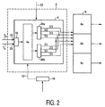
- FIG. 1 An alternative embodiment of the clock generation unit 2 is shown in FIG. in the The difference from the clock generation unit 2 shown in FIG. 1 is the selection register 6 not integrated in the clock generation unit 2.
- the different sentences of switching components 16a, 16b according to FIG. 1 are by the switching component set 16 symbolizes.
- the memory 18 is arranged outside the clock generation unit 2 but also be part of it. Since the selection information in the memory 18 is stored, this is only called up by the clock generation unit 2 when the cell phone is put into operation. To prevent components from being too high Clock frequency and damage are provided, the clock generation unit is provided 2 when starting up with a reference start clock fA with im To be compared to the reference clock fR lower frequency. This is a further input 23 is provided. A clock frequency in the kilohertz range is preferred for this purpose selected, which is intended for an internal clock in the mobile phone.
- the selection information is retrieved from the memory 18 and the selection signal 12 causes the selection of the special circuit parts that the selected Correspond to reference clock fR.
- the selection information is retrieved from the memory 18 and the selection signal 12 causes the selection of the special circuit parts that the selected Correspond to reference clock fR.
- the divider modules 20a, 20b include these special circuit parts the divider modules 20a, 20b.
- a basic setting is provided, in each case for a high Circuit components designed for reference clock for commissioning the clock generation unit 2 are activated. If a lower reference clock fR is selected, then only after Commissioning the circuit parts assigned to this activated.
- the selection signal 12 is transmitted to sub-area 4a of phase-locked loop 4, which is between the switching component set 16 and the divider modules 20a, 20b is arranged.
- one of the two divider modules 20a, 20b selected. With regard to their divider ratios, these are designed so that they at least provide some roughly the same work cycles.
- the outputs of the divider modules 20a, 20b, which provide the same work cycles, are connected to one another and can be called up at the clock generation unit 2 on the output side. At least at some outputs of the clock generation unit 2 are therefore independent of the Input reference frequency the same work cycles.
- the divider module 20a is designed for the 13 MHz operating cycle and has, for example, the divider ratios 5/3, 3/2, 3/3 and 1/5.
- the divider module 20b has the divider ratios 3/3, 2/3, 1/3 and 3/2 and is for a reference clock of about 19.5 MHz, so that of the two divider modules 20a, 20b three approximately approximately the same clock frequencies are provided.
- the of the Clock generation units 2 are provided to the selection register 6 forwarded, which in contrast to FIG. 1 now only the three sub-registers 6a, 6b, 6c. Since at least some outputs of the clock generation unit 2 regardless of the selection made, the same work cycles are available Selection element 14 in the exemplary embodiment according to FIG. 2 is not absolutely necessary.
- a mobile radio system communication device for example in a cell phone, briefly explained.
- This comprises a high-frequency unit 24, which via an antenna 26 Interface to the atmosphere.
- the radio frequency unit 24 is with the reference clock applied to fR and is connected to a microchip 28, as by the double arrow 30 is shown.
- the connection is made via a digital / analog converter, which analog signals of the radio frequency unit 24 into digital signals for the microchip 28 processed and vice versa.
- a so-called switching arrangement is on the microchip 28 Baseband circuit integrated. It has the clock generation unit as a central element 2, which includes a system control processor 32 and a baseband processor 34 a suitable work cycle.
- the baseband processor 34 is for example for the Speech processing is responsible, whereas the system control processor 32 the internal Controls processes within the cell phone.
- the clock generation unit 2 transmits a special one to a time base unit 36 Work cycle, the so-called basic unit cycle.
- the time base unit 36 preferably with a work cycle with a frequency of 4.33 MHz applied.
- the time base unit 36 delivers the precisely defined time frame of the corresponding mobile radio system. This timeframe is divided into several basic units the time base unit 36 divided the two processors 32, 34 in the form of basic unit clocks transmitted.
- the clock generation unit 2 is connected to a clock generator 35a with its input 10 the reference clock fR and with a further input 23 to a clock generator 35b for the reference start clock fA connected.
- the selection of the special reference clock fR takes place via the connection pin 17 on the microchip 28, via which the selection signal 12 to the Clock generation unit 2 is transmitted.
- connection pin 16 Clock generation unit 2 Programming steps on the programmable are also preferred via the connection pin 16 Clock generation unit 2 made.
- the for Time base unit 36 provided basic unit clock with the help of a corresponding Program instruction set.
- the trained for the different reference clocks fR Clock generation unit 2 essentially has the advantage that it is simpler Integrated into existing baseband circuits for different mobile radio systems can be. It is not necessary to use the other components of the baseband circuit to adapt to the clock generation unit 2, since this is independent of Reference clock for suitable work cycles.
- the system control processor 32 is particularly useful for controlling the internal functional sequences connected to a power control unit (power management) 40. Based of the current operational requirements, the system control processor 32 determines which one Work cycle for which component is selected. This information is about the Power control unit 40 forwarded to the clock generation unit 2, which then the delivers corresponding work cycles to the other components. This is done, for example via the selection register 6 shown in FIGS. 1 and 2 via the power control unit 40, the radio frequency unit 24, the clock generator 35a for the reference clock fR and a human-machine interface 42 into a suitable one Operating mode, for example switched to a standby mode. To control the The baseband circuit integrated on the microchip 28 engages internal functional sequences preferably based on information stored in a data memory 44.
Landscapes
- Engineering & Computer Science (AREA)
- Computer Networks & Wireless Communication (AREA)
- Signal Processing (AREA)
- Stabilization Of Oscillater, Synchronisation, Frequency Synthesizers (AREA)
- Transceivers (AREA)
- Mobile Radio Communication Systems (AREA)
Abstract
Description
- Fig. 1
- eine Taktgenerierungseinheit mit einem Phasenregelkreis in einem Blockschaltbild,
- Fig. 2
- eine alternative Taktgenerierungseinheit in einem Blockschaltbild und
- Fig. 3
- ein Blockschaltbild eines Mobilfunksystem-Geräts.
| Teiler-verhältnis | GSM fR = 13MHz | TDMA fR = 19,44 MHz | CDMA fR= 19,66 MHz |
| 6/3 | 26 MHz | 38,88 MHz | 39,36 MHz |
| 5/3 | 21,67 MHz | 32,4 MHz | 32,8 MHz |
| 3/2 | 19,5 MHz | 29,16 MHz | 29,52 MHz |
| 4/3 | 17,33 MHz | 25,92 MHz | 26,24 MHz |
| 3/3 | 13 MHz | 19,44 MHz | 19,68 MHz |
| 2/3 | 8,66 MHz | 12,96 MHz | 13,12 MHz |
| 1/2 | 6,5 MHz | 9,72 MHz | 9,64 MHz |
| 1/3 | 4,33 MHz | 6,48 MHz | 6,56 MHz |
| 1/4 | 3,25 MHz | 4,86 MHz | 4,9 MHz |
Alternativ zu der hardwaretechnischen Ausführung ist eine Softwarefunktionalität vorgesehen, über die das Auswahlsignal 12 übermittelt wird. Hierzu ist beispielsweise gemäß Fig. 2 ein Speicher 18 angeordnet, in dem die Information über den ausgewählten Referenztakt abgelegt ist. Diese Information ist insbesondere überschreibbar.
Claims (22)
- Telekommunikationsgerät mit einer Taktgenerierungseinheit (2), insbesondere für ein Mobilfunksystem, mit einem Eingang (10) für einen Referenztakt (fR), mit einer elektrischen Schaltungsanordnung umfassend einen Phasenregelkreis (4) zur Umwandlung des Referenztakts (fR) in einen Arbeitstakt,
dadurch gekennzeichnet,
dass die Schaltungsanordnung für unterschiedliche Referenztakte (fR) ausgebildete Schaltungsteile (16a, 16b; 20a, 20b) aufweist, und dass einer der Schaltungsteile (16a, 20a) auswählbar ist. - Telekommunikationsgerät mit einer Taktgenerierungseinheit (2) nach Anspruch 1,
dadurch gekennzeichnet,
dass die Schaltungsteile (16a, 16b; 20a, 20b) jeweils ein insbesondere im Phasenregelkreis (4) integriertes Teilermodul (20a, 20b) zur Umwandlung des dem Schaltungsteil (16a, 20a; 16b, 20b) zugeordneten Referenztakts (fR) in mehrere Arbeitstakte aufweisen, und dass die Teilermodule (20a, 20b) derart ausgestaltet sind, dass einige der von ihnen erzeugbaren Arbeitstakte annähernd gleich sind. - Telekommunikationsgerät mit einer Taktgenerierungseinheit (2) nach Anspruch 1,
dadurch gekennzeichnet,
dass der Phasenregelkreis (4) unabhängig vom ausgewählten Schaltungsteil (16a, 16b; 20a, 20b) zur Umwandlung des Referenztakts (fR) in mehrere Arbeitstakte feste Teilerverhältnisse aufweist, und dass ein Auswahlglied (14) vorgesehen ist, das in Abhängigkeit des ausgewählten Referenztakts (fR) bestimmte vom Phasenregelkreis (4) erzeugte Arbeitstakte auswählt. - Telekommunikationsgerät mit einer Taktgenerierungseinheit (2) nach einem der vorhergehenden Ansprüche,
dadurch gekennzeichnet,
dass die Schaltungsteile (16a, 16; 20a, 20b) in Abhängigkeit des Referenztakts (fR) konfigurierbar sind. - Telekommunikationsgerät mit einer Taktgenerierungseinheit (2) nach einem der vorhergehenden Ansprüche,
dadurch gekennzeichnet,
dass der Phasenregelkreis (4) eingangsseitig unterschiedliche auf die Referenztakte (fR) abgestimmte Sätze von Schaltkomponenten (16a, 16b) aufweist, die sein Einschwingverhalten bestimmen und wahlweise aktivierbar sind. - Telekommunikationsgerät mit einer Taktgenerierungseinheit (2) nach einem der Ansprüche 1 bis 5,
dadurch gekennzeichnet,
dass der Phasenregelkreis (4) eingangsseitig einen speziellen Satz von Schaltkomponenten (16) aufweist, der sein Einschwingverhalten bestimmt und zur Verarbeitung mehrerer Referenztakte (fR) geeignet ist. - Telekommunikationsgerät mit einer Taktgenerierungseinheit (2) nach einem der vorhergehenden Ansprüche,
dadurch gekennzeichnet,
dass die Schaltungsteile (16a, 16b; 20a, 20b) zur Bereitstellung zumindest eines annähernd gleichen Arbeitstakts, und insbesondere zur Bereitstellung von fünf annähernd gleichen Arbeitstakten ausgebildet sind. - Telekommunikationsgerät mit einer Taktgenerierungseinheit nach einem der vorhergehenden Ansprüche,
dadurch gekennzeichnet,
dass die bereitgestellten Arbeitstakte über ein Auswahlregister (6) auswählbar sind. - Telekommunikationsgerät mit einer Taktgenerierungseinheit (2) nach einem der vorhergehenden Ansprüche,
dadurch gekennzeichnet,
dass aus den Arbeitstakten ein Grundeinheitentakt insbesondere durch eine programmierbare Software-Funktionalität auswählbar ist. - Telekommunikationsgerät mit einer Taktgenerierungseinheit (2) nach einem der vorhergehenden Ansprüche,
dadurch gekennzeichnet,
dass die Schaltungsanordnung derart ausgelegt ist, dass die Auswahl des dem speziellen Referenztakt (fR) zugeordneten Schaltungsteils (16a, 20a) vor Inbetriebnahme des Phasenregelkreises (4) vorgenommen wird. - Telekommunikationsgerät mit einer Taktgenerierungseinheit (2) nach einem der vorhergehenden Ansprüche,
dadurch gekennzeichnet,
dass sie auf einem Mikrochip (28) integriert ist, und dass einer der Schaltungsteile (16a, 16b; 20a, 20b) durch das Layout des Mikrochips (28) ausgewählt ist. - Telekommunikationsgerät mit einer Taktgenerierungseinheit (2) nach einem der vorhergehenden Ansprüche,
dadurch gekennzeichnet,
dass zur Auswahl des dem speziellen Referenztakt (fR) zugeordneten Schaltungsteils (16a, 20a) ein Anschlusspin (17) zur Übermittlung eines Auswahlsignals vorgesehen ist. - Telekommunikationsgerät mit einer Taktgenerierungseinheit (2) nach einem der vorhergehenden Ansprüche,
dadurch gekennzeichnet,
dass zur Auswahl des dem speziellen Referenztakt (fR) zugeordneten Schaltungsteils eine in die Schaltungsanordnung integrierte Software-Funktionalität vorgesehen ist - Telekommunikationsgerät mit einer Taktgenerierungseinheit (2) nach Anspruch 13,
dadurch gekennzeichnet,
dass ein Register (6) vorgesehen ist , das einen überschreibbaren Registereintrag aufweist, über den die Auswahl des Referenztakts (fR) festgelegt ist. - Telekommunikationsgerät mit einer Taktgenerierungseinheit (2) nach Anspruch 13 oder 14,
dadurch gekennzeichnet,
dass die Schaltungsanordnung einen weiteren Eingang (38) für einen langsamen Referenz-Anfangstakt (fA) aufweist, mit dem der Phasenregelkreis (4) bei seiner Inbetriebnahme verbunden ist. - Telekommunikationsgerät mit einer Taktgenerierungseinheit (2) nach Anspruch 13 oder 14,
dadurch gekennzeichnet,
dass bei Inbetriebnahme des Phasenregelkreises (4) der für einen hohen Referenztakt (fR) ausgebildete Schaltungsteil (16b, 20b) ausgewählt ist. - Taktgenerierungseinheit (2), insbesondere für ein Mobilfunksystem, mit einem Eingang (10) für einen Referenztakt (fR), mit einer elektrischen Schaltungsanordnung umfassend einen Phasenregelkreis (4) zur Umwandlung des Referenztakts (fR) in einen Arbeitstakt,
dadurch gekennzeichnet,
dass die Schaltungsanordnung für unterschiedliche Referenztakte (fR) ausgebildete Schaltungsteile (16a, 16b; 20a, 20b) aufweist, und dass einer der Schaltungsteile (16a, 20a) auswählbar ist. - Verfahren zur Erzeugung eines Arbeitstakts, insbesondere für ein Mobilfunksystem, bei dem ein in einer Schaltungsanordnung integrierter Phasenregelkreis (4) eingangsseitig mit einem Referenztakt (fR) beaufschlagt wird und ausgangsseitig den Arbeitstakt bereitstellt,
dadurch gekennzeichnet,
dass die Schaltungsanordnung für unterschiedliche Referenztakte (fR) ausgebildet ist, und dass die Schaltungsanordnung zumindest einmal auf einen der Referenztakte (fR) abgestimmt wird. - Verfahren nach Anspruch 16,
dadurch gekennzeichnet,
dass die Abstimmung vor der Inbetriebnahme des Phasenregelkreises (4) erfolgt. - Verfahren nach Anspruch 17 oder 18,
dadurch gekennzeichnet,
dass der Schaltungsanordnung über einen Anschlusspin (17) ein Auswahlsignal übermittelt wird, anhand dessen die Abstimmung vorgenommen wird. - Verfahren nach einem der Ansprüche 17 bis 19,
dadurch gekennzeichnet,
dass in einem Auswahlregister (6) zumindest einmalig eine Auswahlinformation über den Referenztakt (fR) abgelegt wird, anhand derer die Abstimmung vorgenommen wird. - Verfahren nach einem der Ansprüche 17 bis 20,
dadurch gekennzeichnet,
dass der Phasenregelkreis (4) zumindest bei seiner Inbetriebnahme mit einem langsamen Referenz-Anfangstakt (fA) beaufschlagt wird, dass anschließend die Abstimmung auf den Referenztakt (fR) erfolgt, und der Phasenregelkreis (4) mit dem Referenztakt (fR) beaufschlagt wird.
Applications Claiming Priority (2)
| Application Number | Priority Date | Filing Date | Title |
|---|---|---|---|
| DE19954696 | 1999-11-13 | ||
| DE19954696A DE19954696A1 (de) | 1999-11-13 | 1999-11-13 | Telekommunikationsgerät mit einer Taktgenerierungseinheit |
Publications (3)
| Publication Number | Publication Date |
|---|---|
| EP1104129A2 true EP1104129A2 (de) | 2001-05-30 |
| EP1104129A3 EP1104129A3 (de) | 2005-08-24 |
| EP1104129B1 EP1104129B1 (de) | 2007-07-11 |
Family
ID=7928965
Family Applications (1)
| Application Number | Title | Priority Date | Filing Date |
|---|---|---|---|
| EP00203913A Expired - Lifetime EP1104129B1 (de) | 1999-11-13 | 2000-11-06 | Telekommunikationsgerät mit einer Taktgenerierungseinheit |
Country Status (4)
| Country | Link |
|---|---|
| US (1) | US6823032B1 (de) |
| EP (1) | EP1104129B1 (de) |
| JP (1) | JP4780258B2 (de) |
| DE (2) | DE19954696A1 (de) |
Families Citing this family (3)
| Publication number | Priority date | Publication date | Assignee | Title |
|---|---|---|---|---|
| US20070230966A1 (en) * | 2006-04-03 | 2007-10-04 | Walsh Peter J | Single interface with automatic rate detection and selection for multiple optical communication standards |
| US9628211B1 (en) * | 2015-06-19 | 2017-04-18 | Amazon Technologies, Inc. | Clock generation with non-integer clock dividing ratio |
| CN114442735B (zh) * | 2020-10-30 | 2023-03-24 | 龙芯中科技术股份有限公司 | 时钟频率控制方法、装置、设备及存储介质 |
Family Cites Families (23)
| Publication number | Priority date | Publication date | Assignee | Title |
|---|---|---|---|---|
| JPS5464956A (en) * | 1977-11-02 | 1979-05-25 | Toshiba Corp | Pll circuit |
| JPH01142227A (ja) * | 1987-11-27 | 1989-06-05 | Japan Electron Control Syst Co Ltd | スロットルセンサの組立方法 |
| US5349544A (en) * | 1988-06-15 | 1994-09-20 | Advanced Micro Devices, Inc. | Programmable system synchronizer |
| JPH02306719A (ja) * | 1989-05-20 | 1990-12-20 | Fujitsu Ltd | クロック供給装置 |
| US5065413A (en) * | 1989-12-09 | 1991-11-12 | Sony Corporation | Phase locked loop circuit |
| JPH03273709A (ja) * | 1990-02-26 | 1991-12-04 | Ricoh Co Ltd | 位相制御回路 |
| JPH06268551A (ja) * | 1993-03-11 | 1994-09-22 | Toshiba Corp | シンセサイザ回路 |
| JP3344790B2 (ja) * | 1993-10-28 | 2002-11-18 | アイコム株式会社 | 周波数シンセサイザ |
| JP3180865B2 (ja) * | 1994-06-10 | 2001-06-25 | 株式会社富士通ゼネラル | 適応型pll回路 |
| GB9414729D0 (en) * | 1994-07-21 | 1994-09-07 | Mitel Corp | Digital phase locked loop |
| KR0177731B1 (ko) * | 1994-09-15 | 1999-05-15 | 정장호 | 망동기용 디지탈 위상동기루프 제어방법 |
| JPH08204545A (ja) * | 1995-01-30 | 1996-08-09 | Sony Tektronix Corp | 分周回路 |
| JP3393954B2 (ja) * | 1995-05-16 | 2003-04-07 | 松下電器産業株式会社 | 時分割多重fdd/tddデュアルモード無線機 |
| JP3183812B2 (ja) * | 1995-10-16 | 2001-07-09 | 株式会社エヌ・ティ・ティ・ドコモ | 移動無線機のマルチバンド高周波回路 |
| JPH09153800A (ja) * | 1995-11-29 | 1997-06-10 | Kokusai Electric Co Ltd | 周波数シンセサイザ |
| US5630222A (en) * | 1995-12-04 | 1997-05-13 | Motorola Inc. | Method and apparatus for generating multiple signals at multiple frequencies |
| JP3830225B2 (ja) * | 1997-03-28 | 2006-10-04 | ローム株式会社 | IrDA変復調IC |
| JPH11143573A (ja) * | 1997-11-10 | 1999-05-28 | Fujitsu Ltd | クロック供給方法及び情報処理装置 |
| US6308048B1 (en) * | 1997-11-19 | 2001-10-23 | Ericsson Inc. | Simplified reference frequency distribution in a mobile phone |
| US6282184B1 (en) * | 1997-12-22 | 2001-08-28 | Nortel Networks Limited | Common digitizing rate for multiple air interfaces for generic cell sites in cellular radio |
| JP3556464B2 (ja) * | 1998-03-30 | 2004-08-18 | 株式会社東芝 | マルチモード無線機の通話断防止方法 |
| JPH11308096A (ja) * | 1998-04-24 | 1999-11-05 | Ando Electric Co Ltd | 位相ロックループ回路 |
| US6194939B1 (en) * | 1999-09-21 | 2001-02-27 | Alcatel | Time-walking prevention in a digital switching implementation for clock selection |
-
1999
- 1999-11-13 DE DE19954696A patent/DE19954696A1/de not_active Withdrawn
-
2000
- 2000-11-06 DE DE50014471T patent/DE50014471D1/de not_active Expired - Lifetime
- 2000-11-06 EP EP00203913A patent/EP1104129B1/de not_active Expired - Lifetime
- 2000-11-13 JP JP2000344963A patent/JP4780258B2/ja not_active Expired - Lifetime
- 2000-11-13 US US09/711,230 patent/US6823032B1/en not_active Expired - Lifetime
Also Published As
| Publication number | Publication date |
|---|---|
| JP4780258B2 (ja) | 2011-09-28 |
| DE19954696A1 (de) | 2001-05-17 |
| EP1104129B1 (de) | 2007-07-11 |
| DE50014471D1 (de) | 2007-08-23 |
| EP1104129A3 (de) | 2005-08-24 |
| US6823032B1 (en) | 2004-11-23 |
| JP2001177396A (ja) | 2001-06-29 |
Similar Documents
| Publication | Publication Date | Title |
|---|---|---|
| DE3750810T2 (de) | Frequenzsynthetisierer. | |
| DE60209922T2 (de) | Dual mode bluetooth/wireless gerät mit optimierten aufwach-zeiten für energie-einsparung | |
| DE69229819T2 (de) | Einstellung der Taktfrequenz einer elektrischen Schaltung | |
| DE102008062015A1 (de) | RF-Transceiver, Kommunikationsvorrichtung und Verfahren zum Steuern eines RF-Transceivers | |
| DE69423837T2 (de) | Taktversorgungssystem | |
| DE102004044099B4 (de) | Streuspektrum-Taktgeber, Speichersystem und Taktsignalverzögerungsverfahren | |
| EP1104129B1 (de) | Telekommunikationsgerät mit einer Taktgenerierungseinheit | |
| DE10241385A1 (de) | Integrierter Schaltkreis | |
| DE19815944C2 (de) | Energiesparschaltung für ein elektronisches Gerät und Steuerverfahren zur Energieeinsparung in einem elektronischen Gerät | |
| DE60120490T2 (de) | Phasenregelschleife | |
| DE19837204B4 (de) | Totzeitreduzierung bei Frequenzsprüngen in Mehrfachbandsyntheseeinheiten | |
| EP1602178B1 (de) | Vorrichtung und Verfahren zum steuern des Leistungsverbrauchs einer kombinierten UMTS/GSM/EDGE-Funkstation | |
| EP1046125B1 (de) | Datenträger | |
| DE102009050977A1 (de) | Taktsteuerung für eine Datensynchronisation in Varaktorarrays | |
| DE19706496A1 (de) | Taktversorgungssystem für ein Microcomputersystem | |
| EP1110300A1 (de) | Energieversorgungseinrichtung und schaltungsanordnung mit dieser energieversorgungseinrichtung | |
| WO2004049619A1 (de) | Verfahren zur automatischen erkennung der taktfrequenz eines systemtaktes für die konfiguration einer peripherie-einrichtung | |
| EP1444781B1 (de) | Verfahren zur vermeidung von transienten bei schaltvorgängen in integrierten schaltkreisen sowie integrierter schaltkreis | |
| EP0898372B1 (de) | Verfahren und Vorrichtung zum Einstellen der Schwingfrequenz eines Oszillators | |
| DE19736463C2 (de) | Verfahren und Vorrichtung zum Einstellen der Schwingfrequenz eines Oszilators | |
| EP0760560A2 (de) | Funkeinrichtung, bestehend aus einer Mobilfunkeinheit und einer Funkuhr | |
| DE60000054T2 (de) | Vorrichtung und Verfahren zum Sichern der Zeitinformation in einem Mobiltelephon | |
| DE102012015943B4 (de) | Initialzellsuchverfahren und entsprechendes Anwendergerät und entsprechender Chip | |
| DE102004004808A1 (de) | Verfahren und Vorrichtung zum Sichern und Einstellen eines Schaltungszustandes einer mikroelektronischen Schaltung | |
| EP1347578B1 (de) | Taktschema und Takteinrichtung für eine monolitisch integrierte Schaltung |
Legal Events
| Date | Code | Title | Description |
|---|---|---|---|
| PUAI | Public reference made under article 153(3) epc to a published international application that has entered the european phase |
Free format text: ORIGINAL CODE: 0009012 |
|
| AK | Designated contracting states |
Kind code of ref document: A2 Designated state(s): AT BE CH CY DE DK ES FI FR GB GR IE IT LI LU MC NL PT SE TR |
|
| AX | Request for extension of the european patent |
Free format text: AL;LT;LV;MK;RO;SI |
|
| RAP1 | Party data changed (applicant data changed or rights of an application transferred) |
Owner name: PHILIPS CORPORATE INTELLECTUAL PROPERTY GMBH Owner name: KONINKLIJKE PHILIPS ELECTRONICS N.V. |
|
| RAP1 | Party data changed (applicant data changed or rights of an application transferred) |
Owner name: PHILIPS INTELLECTUAL PROPERTY & STANDARDS GMBH Owner name: KONINKLIJKE PHILIPS ELECTRONICS N.V. |
|
| PUAL | Search report despatched |
Free format text: ORIGINAL CODE: 0009013 |
|
| AK | Designated contracting states |
Kind code of ref document: A3 Designated state(s): AT BE CH CY DE DK ES FI FR GB GR IE IT LI LU MC NL PT SE TR |
|
| AX | Request for extension of the european patent |
Extension state: AL LT LV MK RO SI |
|
| RIC1 | Information provided on ipc code assigned before grant |
Ipc: 7H 04L 7/033 B Ipc: 7H 03L 7/08 B Ipc: 7H 04J 3/06 A Ipc: 7H 04B 7/26 B |
|
| 17P | Request for examination filed |
Effective date: 20060224 |
|
| AKX | Designation fees paid |
Designated state(s): DE FR GB |
|
| GRAP | Despatch of communication of intention to grant a patent |
Free format text: ORIGINAL CODE: EPIDOSNIGR1 |
|
| GRAS | Grant fee paid |
Free format text: ORIGINAL CODE: EPIDOSNIGR3 |
|
| GRAA | (expected) grant |
Free format text: ORIGINAL CODE: 0009210 |
|
| AK | Designated contracting states |
Kind code of ref document: B1 Designated state(s): DE FR GB |
|
| REG | Reference to a national code |
Ref country code: GB Ref legal event code: FG4D Free format text: NOT ENGLISH |
|
| RAP2 | Party data changed (patent owner data changed or rights of a patent transferred) |
Owner name: NXP B.V. |
|
| REF | Corresponds to: |
Ref document number: 50014471 Country of ref document: DE Date of ref document: 20070823 Kind code of ref document: P |
|
| GBT | Gb: translation of ep patent filed (gb section 77(6)(a)/1977) |
Effective date: 20071003 |
|
| ET | Fr: translation filed | ||
| PLBE | No opposition filed within time limit |
Free format text: ORIGINAL CODE: 0009261 |
|
| STAA | Information on the status of an ep patent application or granted ep patent |
Free format text: STATUS: NO OPPOSITION FILED WITHIN TIME LIMIT |
|
| 26N | No opposition filed |
Effective date: 20080414 |
|
| REG | Reference to a national code |
Ref country code: GB Ref legal event code: 732E |
|
| REG | Reference to a national code |
Ref country code: FR Ref legal event code: TP |
|
| REG | Reference to a national code |
Ref country code: FR Ref legal event code: PLFP Year of fee payment: 16 |
|
| REG | Reference to a national code |
Ref country code: FR Ref legal event code: PLFP Year of fee payment: 17 |
|
| REG | Reference to a national code |
Ref country code: FR Ref legal event code: PLFP Year of fee payment: 18 |
|
| REG | Reference to a national code |
Ref country code: FR Ref legal event code: PLFP Year of fee payment: 19 |
|
| PGFP | Annual fee paid to national office [announced via postgrant information from national office to epo] |
Ref country code: DE Payment date: 20191021 Year of fee payment: 20 |
|
| PGFP | Annual fee paid to national office [announced via postgrant information from national office to epo] |
Ref country code: FR Payment date: 20191022 Year of fee payment: 20 |
|
| PGFP | Annual fee paid to national office [announced via postgrant information from national office to epo] |
Ref country code: GB Payment date: 20191022 Year of fee payment: 20 |
|
| REG | Reference to a national code |
Ref country code: DE Ref legal event code: R071 Ref document number: 50014471 Country of ref document: DE |
|
| REG | Reference to a national code |
Ref country code: GB Ref legal event code: PE20 Expiry date: 20201105 |
|
| PG25 | Lapsed in a contracting state [announced via postgrant information from national office to epo] |
Ref country code: GB Free format text: LAPSE BECAUSE OF EXPIRATION OF PROTECTION Effective date: 20201105 |