EP1102467B1 - Appareil de formation d'images a semi-conducteurs, methode de commande de celui-ci et peripherique d'entree d'image - Google Patents
Appareil de formation d'images a semi-conducteurs, methode de commande de celui-ci et peripherique d'entree d'image Download PDFInfo
- Publication number
- EP1102467B1 EP1102467B1 EP00935594A EP00935594A EP1102467B1 EP 1102467 B1 EP1102467 B1 EP 1102467B1 EP 00935594 A EP00935594 A EP 00935594A EP 00935594 A EP00935594 A EP 00935594A EP 1102467 B1 EP1102467 B1 EP 1102467B1
- Authority
- EP
- European Patent Office
- Prior art keywords
- row
- light
- charge transfer
- receiving pixel
- output mode
- Prior art date
- Legal status (The legal status is an assumption and is not a legal conclusion. Google has not performed a legal analysis and makes no representation as to the accuracy of the status listed.)
- Expired - Lifetime
Links
Images


Classifications
-
- H—ELECTRICITY
- H04—ELECTRIC COMMUNICATION TECHNIQUE
- H04N—PICTORIAL COMMUNICATION, e.g. TELEVISION
- H04N25/00—Circuitry of solid-state image sensors [SSIS]; Control thereof
- H04N25/40—Extracting pixel data from image sensors by controlling scanning circuits, e.g. by modifying the number of pixels sampled or to be sampled
- H04N25/46—Extracting pixel data from image sensors by controlling scanning circuits, e.g. by modifying the number of pixels sampled or to be sampled by combining or binning pixels
-
- H—ELECTRICITY
- H04—ELECTRIC COMMUNICATION TECHNIQUE
- H04N—PICTORIAL COMMUNICATION, e.g. TELEVISION
- H04N25/00—Circuitry of solid-state image sensors [SSIS]; Control thereof
- H04N25/70—SSIS architectures; Circuits associated therewith
- H04N25/71—Charge-coupled device [CCD] sensors; Charge-transfer registers specially adapted for CCD sensors
- H04N25/713—Transfer or readout registers; Split readout registers or multiple readout registers
-
- H—ELECTRICITY
- H04—ELECTRIC COMMUNICATION TECHNIQUE
- H04N—PICTORIAL COMMUNICATION, e.g. TELEVISION
- H04N25/00—Circuitry of solid-state image sensors [SSIS]; Control thereof
- H04N25/70—SSIS architectures; Circuits associated therewith
- H04N25/71—Charge-coupled device [CCD] sensors; Charge-transfer registers specially adapted for CCD sensors
- H04N25/745—Circuitry for generating timing or clock signals
Definitions
- the present invention relates to a solid-state image pick-up apparatus and to a driving method therefor, each in accordance with the precharacterizing parts of independent claims 1 and 2 and to an image input apparatus using the solid-state image pick-up apparatus.
- a solid-state image pick-up apparatus and a driving method therefor of that kind are disclosed in US-A-4,712,137.
- An image input apparatus that is applied to a scanner or a copier uses a solid-state image pick-up apparatus having a linear sensor, and inputs an image, by scanning the read position of the solid-state image pick-up apparatus.
- the linear sensor As well, there has hitherto been developed the one that copes with such demand by using a plurality of sensor rows.
- the solid-state image pick-up apparatus comprising two rows of sensors, one of the sensor rows and the other of them are arranged so as to be displaced from each other by a half pitch of the pixels.
- the electric charges acquired by one of the sensor rows and the electric charges acquired by the other of them may be multiplexed and alternately outputted.
- the timing of a reset pulse signal for causing discharge of the electric charges of a floating diffusion amplifier that is electric-charge/voltage conversion means is controlled so that the electric charges acquired from the pixels by both of the sensor rows and alternately transferred to the floating diffusion amplifier may be added there to each other and outputted therefrom.
- accumulation i.e. addition of the electric charges that have been transferred by the second charge transfer row.
- the electric charges that have been transferred by the first charge transfer row to the multiplex section are sent.
- accumulation i.e. addition of the electric charges that have been transferred by the first charge transfer row until a transfer time when the electric charges to be added to each other are transferred by the second charge transfer row comes.
- FIG. 1 is a schematic diagram illustrating a solid-state image pick-up apparatus according to this embodiment
- FIG. 2 is a schematic diagram illustrating a main part of the solid-state image pick-up apparatus according to this embodiment
- FIGS. 3 and 4 are timing charts illustrating a driving method of the solid-state image pick-up apparatus according to this embodiment.
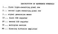
- the solid-state image pick-up apparatus of this embodiment comprises a first CCD register 10 and a second CCD register 20 that are each provided correspondingly to two sensor rows, i.e. a first light-receiving pixel row and a second light-receiving pixel row and a multiplex section 30 that, depending on the relevant output mode, transfers each of the electric charges that have been transferred from the first CCD register 10 and second CCD register 20.
- Transfer elements forming the first CCD register 10, second CCD register 20, and multiplex section 30 are each made so that the potential of part of the area on the side where electric charge is output may become higher than that of the remaining area.
- the solid-state image pick-up apparatus of this embodiment comprises signal generation means 3 for supplying a pulse signal to the first CCD register 10, second CCD register 20, multiplex section 30, etc. with predetermined timings.
- This solid-state image pick-up apparatus has the two following output modes.
- One is an alternately-output mode in which the electric charge that has been individually acquired by respective two sensor rows is alternately transferred from the multiplex section 30, and then a floating diffusion amplifier FD that is connected thereto in the succeeding stage alternately outputs the signals correspond to the respective electrical charges.
- the other is an add-and-output mode in which, of the electric charges acquired by the two sensor rows, the ones obtained from adjacent pixels in the same sensor row are added together and then outputted.
- the first light-receiving pixel row and second light-receiving pixel row forming the two rows of sensors are arranged in a manner of being displaced by a half pitch of the pixel. Alternately outputting the respective electric charges acquired by the two rows of sensors in the alternately output mode enables reading an image with a resolution twice the pitch of pixels of one row with regard to the direction of the pixel row.
- the add-and-output mode the electric charges acquired from adjacent pixels in the same row are added to each other and the resulting signal is outputted. Therefore, reading of an image is performed with a resolution half the pitch of pixels of one row.
- the already added electric charges are transferred to the floating diffusion amplifier FD, it is possible to obtain a signal output in which the electric charges of adjacent pixels are mutually added with the same timing as in the alternately-output mode.
- a pulse signal can be independently impressed to a final stage of the second CCD register 20. In accordance with the timing of impressing the pulse signal to that final stage, changeover of the output modes is performed.
- the first CCD register 10 is alternately impressed with pulse signals consisting of ⁇ 1 and ⁇ 2, while the second CCD register 20 is alternately impressed with pulse signals of ⁇ 2 and ⁇ 1. Further, a pulse signal of ⁇ 1' is independently impressed to the final stage of the second CCD register 20.
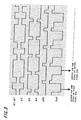
- FIG. 3 is a timing chart in the case of the alternately-output mode.
- signals ⁇ 1, ⁇ 2 in opposite phases to each other are impressed to the first CCD register 10 and the second CCD register 20, respectively.
- the same pulse signal ⁇ 1' as the pulse signal ⁇ 1 is impressed to the final stage of the second CCD register 20.
- signals ⁇ 3, ⁇ 4 in opposite phases to each other are impressed.
- the signals ⁇ 3, ⁇ 4 each have a frequency twice that of the signals ⁇ 1, ⁇ 2.
- the electric charges obtained by the first light-receiving pixel row and the electric charges obtained by the second light-receiving, pixel row, which are alternately transferred from the first CCD register 10 and the second CCD register 20, are sequentially transferred toward the floating diffusion amplifier FD.
- This driving enables the following operation.
- a signal corresponding to one pixel of the first pixel row and a signal corresponding to one pixel of the second pixel row can alternately be outputted from the floating diffusion amplifier FD.
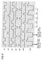
- FIG. 4 is a timing chart in case of the add-and-output mode.
- the signals ⁇ 1, ⁇ 2 in opposite phases to each other are impressed to the first CCD register 10 and the second CCD register 20, respectively.
- the pulse signal ⁇ 1' impressed to the final stage of the second CCD register 20 is made to have a high level only once during a time period in which the ⁇ 1 has a high level consecutively twice.
- the pulse signal ⁇ 3 is made to have a high level, so that the electric charges corresponding to two adjacent pixels transferred from the first CCD register 10 according to the pulse signals ⁇ 1, ⁇ 2 are added to each other at a section (c) illustrated in FIG. 2. Thereafter, the ⁇ 3 is made to have a high level -> low level -> high level (the ⁇ 4 is made to have a low level -> high level -> low level). By doing so, it will be possible to transfer the previously added electric charges to a section (b) illustrated in FIG. 2.
- the ⁇ 1' is made to have a low level and the ⁇ 1 is made to have a high level -> low level -> high level (the ⁇ 2 is made to have a low level -> high level -> low level).
- the electric charges corresponding to two adjacent pixels transferred from the second CCD register 20 are added to each other at a portion (d) illustrated in FIG. 2.
- the ⁇ 3 is made to have a high level -> low level -> high level (the ⁇ 4 is made to have a low level -> high level -> low level).
- the resulting electric charge obtained by adding to each other the electric charges from two adjacent pixels that have been transferred from the first CCD register 10 to the portion (b) illustrated in FIG. 2 are transferred to a portion (a).
- the ⁇ 1' is made to have a low level -> high level (during this period of time the ⁇ 3 is made to have a high level).
- the resulting electric charges corresponding to two adjacent pixels transferred from the second CCD register 20, and mutually added at the portion (d) in FIG. 2 are transferred to the portion (c) illustrated in FIG. 2.
- the ⁇ 3 is made to have a high level -> low level -> high level (the 04 is made to have a low level -> high level -> low level).
- the electric charges obtained by adding to each other the electric charges from two adjacent pixels that have been transferred from the second CCD register 20 can be transferred to the portion (b) illustrated in FIG. 2.
- This driving enables finally the floating diffusion amplifier FD, to alternately output correspondingly to the time period 1 ⁇ and the time period 2 ⁇ two-pixel added signal for the first light-receiving pixel row and two-pixel added signal for the second light-receiving pixel row in the order above mentioned.
- the above-described solid-state image pick-up apparatus and its driving method are mainly applied to the image input apparatus such as a scanner or a copier.
- the image input apparatus such as a scanner or a copier.
- it is arranged to obtain the respective pixel outputs that have been acquired by the first light-receiving pixel row and the second light-receiving pixel row according to the previously described alternately-output mode.
- the solid-state image pick-up apparatus, the driving method therefor, and the image input apparatus according to the present invention have the following advantages.
- the multiplexing structure type of solid-state image pick-up apparatus addition of the electric charges from adjacent pixels in the same light-receiving pixel row can be performed through a simple pulse change.
- With the use of a single solid-state image pick-up apparatus it is possible to cope with the demands both high resolution and high-speed signal processing and satisfy a wide variety of needs. As a result, it is possible in turn to reduce the manufacturing cost of the solid-state image pick-up apparatus that can cope with the demands both for high resolution and high-speed signal processing.
Landscapes
- Engineering & Computer Science (AREA)
- Multimedia (AREA)
- Signal Processing (AREA)
- Solid State Image Pick-Up Elements (AREA)
- Transforming Light Signals Into Electric Signals (AREA)
- Facsimile Heads (AREA)
Abstract
Claims (3)
- Dispositif de prise de vue d'image à l'état solide comprenant :caractérisé en ce que ledit dispositif de prise de vue d'image aune première rangée de transfert de charges (10) pour transférer des charges électriques acquises par une première rangée de pixels de réception de lumière (1) ;une seconde rangée de transfert de charges (20) pour transférer des charges électriques acquises par une seconde rangée de pixels de réception de lumière (2) ;une section de multiplexage (30) pour transférer les charges électriques respectives transférées à partir de la première rangée de transfert de charges (10) et une seconde rangée de transfert de charges (20) vers un moyen de conversion charge/tension électrique (FD), etun moyen de génération de signal (3) pour fournir des signaux d'impulsion (1, 2, 1' , 3, 4, RS) à ladite première rangée de transfert de charges (10) à ladite seconde rangée de transfert de charges (20), à ladite section de multiplexage (30) et auxdits moyens de conversion de charges/tension électrique (FD) avec des temporisations prédéterminées, respectivement, ladite première rangée de pixels de réception de lumière (1) et ladite seconde rangée de pixels de réception de lumière (2) étant disposées l'une contre l'autre par un demi-pas de pixels de celles-ci,
un mode de sortie en alternance dans lequel les charges électriques qui ont été individuellement acquises par chacune des première et seconde rangées de pixels de réception de lumière (1, 2) sont transférées en alternance à partir de la section de multiplexage (30) et puis délivrées, et
un mode d'addition et de sortie dans lequel à partir des charges électriques acquises par les première et seconde rangées de réception de lumière (1, 2) celles obtenues à partir des pixels adjacents dans la même rangée de pixels de réception de lumière (1, 2) sont ajoutées ensemble et puis délivrées, et
ledit moyen de génération de signal (3) étant disposé et raccordé à ladite première rangée de transfert de charges (10, 20) pour
dans les deux modes de sortie application des premier et second signaux d'impulsion (1, 2) de phases opposées l'une à l'autre en alternance à ladite première et seconde rangées de transfert de charges (10, 20) et un autre signal d'impulsion (1') indépendamment à l'étage final de ladite seconde rangée de transfert de charges (20) et pour réaliser l'inversion entre ledit mode de sortie en alternance et ledit mode d'addition et de sortie selon la temporisation de sortie desdits signaux d'impulsion, dans lequel
pour ledit mode de sortie en alternance ledit moyen de génération de signal (3) applique ledit autre signal d'impulsion (1') identique audit premier signal d'impulsion (1') audit étage final de ladite seconde rangée de transfert de charges (20), et
pour ledit mode d'addition et de sortie, ledit moyen de génération de signal (3) applique ledit autre signal d'impulsion (1') ayant un niveau élevé seulement une fois pendant une période de temps pendant laquelle le premier signal d'impulsion (1') a un niveau élevé consécutivement double pour accumuler les charges électriques jusqu'à ce qu'un temps de transfert arrive où les charges électriques à ajouter l'une à l'autre sont transférées par la seconde rangée de transfert de charges (20). - Procédé de commande pour commander un dispositif de prise de vue d'image à l'état solide, comprenant :une première rangée de transfert de charges (10) pour transférer des charges électriques acquises par une première rangée de pixels de réception de lumière (1) ;une seconde rangée de transfert de charges pour transférer des charges électriques acquises par une seconde rangée de pixels de réception de lumière (2) etune section de multiplexage (30) pour transférer les charges électriques respectives transférées à partir desdites première et seconde rangées de transfert de charges (10, 20) à un moyen de conversion de conversion charges/tension électrique (FD) dans lequel
ladite première rangée de pixels de réception de lumière (1) et ladite seconde rangée de pixels de réception de lumière (2) sont déplacées par rapport l'une à l'autre d'un demi-pas de pixels de celles-ci, caractérisé par les étapes suivantes :application des premier et second signaux d'impulsion (1, 2) de phase opposée l'une à l'autre en alternance auxdites première et seconde rangées de transfert de charges (10, 20) et un autre signal d'impulsion (1') indépendamment de l'étage final de ladite seconde rangée de transfert de charges (20) ;inversion entre un mode de sortie en alternance dans lequel les charges électriques qui ont été individuellement acquises par chacune des première et seconde rangées de pixels de réception de lumière (1, 2) sont transférées en alternance à partir de la section de multiplexage (30) et puis délivrées, et un mode d'addition et de sortie dans lequel les charges électriques acquises par les première et seconde rangées de pixels de réception de lumière (1, 2) celles obtenues à partir des pixels adjacentes dans la même rangée de pixels de réception de lumière (1, 2) sont ajoutées ensemble et puis délivrées,dans le cas dudit mode de sortie en alternance application dudit autre signal d'impulsion (1') identique audit signal d'impulsion (1) audit étage final de ladite seconde rangée de transfert de charges (20), etdans le cas dudit mode d'addition et de sortie application dudit autre signal d'impulsion (1') ayant un niveau élevé seulement une fois pendant une période de temps pendant où le premier signal d'impulsion (1) a un niveau élevé consécutivement double pour accumuler les charges électriques jusqu'à ce qu'un temps de transfert arrive avec lequel les charges électriques à ajouter les unes aux autres soient transférées par la seconde rangée de transfert de charges (20). - Dispositif d'entrée d'image caractérisé par l'utilisation d'un dispositif de prise de vue à l'état solide selon la revendication 1.
Applications Claiming Priority (5)
| Application Number | Priority Date | Filing Date | Title |
|---|---|---|---|
| JP16216099 | 1999-06-09 | ||
| JP16216099 | 1999-06-09 | ||
| JP2000162289 | 2000-05-31 | ||
| JP2000162289A JP4419275B2 (ja) | 1999-06-09 | 2000-05-31 | 固体撮像装置およびその駆動方法並びに画像入力装置 |
| PCT/JP2000/003735 WO2000076200A1 (fr) | 1999-06-09 | 2000-06-08 | Appareil de formation d'images a semi-conducteurs, methode de commande de celui-ci et peripherique d'entree d'image |
Publications (3)
| Publication Number | Publication Date |
|---|---|
| EP1102467A1 EP1102467A1 (fr) | 2001-05-23 |
| EP1102467A4 EP1102467A4 (fr) | 2001-10-04 |
| EP1102467B1 true EP1102467B1 (fr) | 2005-05-25 |
Family
ID=26488054
Family Applications (1)
| Application Number | Title | Priority Date | Filing Date |
|---|---|---|---|
| EP00935594A Expired - Lifetime EP1102467B1 (fr) | 1999-06-09 | 2000-06-08 | Appareil de formation d'images a semi-conducteurs, methode de commande de celui-ci et peripherique d'entree d'image |
Country Status (5)
| Country | Link |
|---|---|
| US (1) | US6744539B1 (fr) |
| EP (1) | EP1102467B1 (fr) |
| JP (1) | JP4419275B2 (fr) |
| DE (1) | DE60020324T2 (fr) |
| WO (1) | WO2000076200A1 (fr) |
Families Citing this family (4)
| Publication number | Priority date | Publication date | Assignee | Title |
|---|---|---|---|---|
| US6770860B1 (en) * | 2000-02-14 | 2004-08-03 | Dalsa, Inc. | Dual line integrating line scan sensor |
| JP3832661B2 (ja) * | 2003-12-12 | 2006-10-11 | ソニー株式会社 | 固体撮像装置の駆動方法 |
| JP5181840B2 (ja) * | 2008-05-30 | 2013-04-10 | ソニー株式会社 | 固体撮像装置、固体撮像装置の駆動方法、及び電子機器 |
| JP2024022190A (ja) * | 2022-08-05 | 2024-02-16 | 株式会社東芝 | 信号処理装置、光検出器、及び距離計測装置 |
Family Cites Families (16)
| Publication number | Priority date | Publication date | Assignee | Title |
|---|---|---|---|---|
| US4712137A (en) * | 1981-07-20 | 1987-12-08 | Xerox Corporation | High density CCD imager |
| US4432017A (en) * | 1981-07-20 | 1984-02-14 | Xerox Corporation | Adjacent bilinear photosite imager |
| US4438457A (en) * | 1981-07-20 | 1984-03-20 | Xerox Corporation | High resolution imager employing staggered sensor structure |
| JPS58190169A (ja) * | 1982-04-30 | 1983-11-07 | Toshiba Corp | 固体撮像装置 |
| CA1219337A (fr) | 1983-08-22 | 1987-03-17 | Peter A. Levine | Camera a dispositif a transfert de charge a bruit reduit avec echantillonnage simple du signal de sortie |
| JP2868915B2 (ja) | 1991-03-27 | 1999-03-10 | 株式会社東芝 | 固体撮像装置 |
| JP2973650B2 (ja) | 1991-10-08 | 1999-11-08 | ソニー株式会社 | 電荷転送装置の出力回路 |
| CA2060556A1 (fr) | 1992-02-03 | 1993-08-04 | Savvas G. Chamberlain | Structure de sortie haute frequence bimode a differenciation de pixels montee sur une puce de capteur d'image a transfert de charge |
| JP2968898B2 (ja) * | 1993-02-23 | 1999-11-02 | シャープ株式会社 | 読取り装置 |
| US5751444A (en) * | 1995-12-18 | 1998-05-12 | Adobe Systems Incorporated | Imaging apparatus for copying bound documents |
| JPH09219824A (ja) | 1996-02-09 | 1997-08-19 | Sony Corp | 固体撮像装置 |
| JPH09321953A (ja) * | 1996-05-28 | 1997-12-12 | Sanyo Electric Co Ltd | 撮像装置 |
| JPH10285343A (ja) * | 1997-04-09 | 1998-10-23 | Canon Inc | 画像処理装置及び画像処理方法 |
| JPH11164087A (ja) * | 1997-11-28 | 1999-06-18 | Sony Corp | 固体撮像装置およびその駆動方法 |
| US6166831A (en) * | 1997-12-15 | 2000-12-26 | Analog Devices, Inc. | Spatially offset, row interpolated image sensor |
| US6462779B1 (en) * | 1998-02-23 | 2002-10-08 | Eastman Kodak Company | Constant speed, variable resolution two-phase CCD |
-
2000
- 2000-05-31 JP JP2000162289A patent/JP4419275B2/ja not_active Expired - Fee Related
- 2000-06-08 EP EP00935594A patent/EP1102467B1/fr not_active Expired - Lifetime
- 2000-06-08 WO PCT/JP2000/003735 patent/WO2000076200A1/fr not_active Ceased
- 2000-06-08 DE DE60020324T patent/DE60020324T2/de not_active Expired - Lifetime
- 2000-06-08 US US09/762,623 patent/US6744539B1/en not_active Expired - Fee Related
Also Published As
| Publication number | Publication date |
|---|---|
| JP4419275B2 (ja) | 2010-02-24 |
| WO2000076200A1 (fr) | 2000-12-14 |
| JP2001057622A (ja) | 2001-02-27 |
| US6744539B1 (en) | 2004-06-01 |
| EP1102467A1 (fr) | 2001-05-23 |
| EP1102467A4 (fr) | 2001-10-04 |
| DE60020324D1 (de) | 2005-06-30 |
| DE60020324T2 (de) | 2006-04-27 |
Similar Documents
| Publication | Publication Date | Title |
|---|---|---|
| US20020071046A1 (en) | Solid-state image apparatus, driving method therefor, and camera system | |
| EP1110372B1 (fr) | Appareil de lecture optique equipe d'une resolution commutable | |
| JPH06245147A (ja) | 固体撮像装置及び固体撮像装置の駆動方法 | |
| EP1102467B1 (fr) | Appareil de formation d'images a semi-conducteurs, methode de commande de celui-ci et peripherique d'entree d'image | |
| US8045025B2 (en) | Image pickup device adaptable to display fewer vertical pixels | |
| KR100415215B1 (ko) | 고체촬상장치,그구동방법및고체촬상장치를사용한카메라 | |
| JP3102348B2 (ja) | カラーリニアイメージセンサおよびその駆動方法 | |
| CN101232558B (zh) | 固态成像设备 | |
| JP3581554B2 (ja) | イメージセンサ及び画像読取装置 | |
| JPH0834564B2 (ja) | 固体撮像装置およびその駆動方法 | |
| JPH11234473A (ja) | 光電変換装置及び密着型イメージセンサと画像読取装置 | |
| JP4269431B2 (ja) | 固体撮像装置およびその駆動方法並びに画像入力装置 | |
| JP2002185871A (ja) | 固体撮像素子及びその駆動方法 | |
| JP3964567B2 (ja) | 固体撮像装置 | |
| JP3089507B2 (ja) | 固体撮像素子および信号電荷転送方法 | |
| JP2010004577A (ja) | 固体撮像装置およびその駆動方法並びに画像入力装置 | |
| US6355949B1 (en) | Solid state imaging apparatus with horizontal charge transfer register which can transfer signal charge faster | |
| JPH11164205A (ja) | 固体撮像装置およびその駆動方法 | |
| JP3149909B2 (ja) | イメージセンサ | |
| JPH11164087A (ja) | 固体撮像装置およびその駆動方法 | |
| JP4082276B2 (ja) | 撮像装置及びその駆動方法 | |
| US7586133B2 (en) | Solid state imaging apparatus and driving method of solid state imaging apparatus | |
| JP2001157119A (ja) | 固体撮像装置の駆動方法 | |
| JPH11266401A (ja) | 固体撮像素子 | |
| JPS5834996B2 (ja) | カラ−コタイサツゾウソウチ |
Legal Events
| Date | Code | Title | Description |
|---|---|---|---|
| PUAI | Public reference made under article 153(3) epc to a published international application that has entered the european phase |
Free format text: ORIGINAL CODE: 0009012 |
|
| 17P | Request for examination filed |
Effective date: 20010221 |
|
| AK | Designated contracting states |
Kind code of ref document: A1 Designated state(s): AT BE CH CY DE DK ES FI FR GB GR IE IT LI LU MC NL PT SE |
|
| AX | Request for extension of the european patent |
Free format text: AL;LT;LV;MK;RO;SI |
|
| A4 | Supplementary search report drawn up and despatched |
Effective date: 20010817 |
|
| AK | Designated contracting states |
Kind code of ref document: A4 Designated state(s): AT BE CH CY DE DK ES FI FR GB GR IE IT LI LU MC NL PT SE |
|
| RIC1 | Information provided on ipc code assigned before grant |
Free format text: 7H 04N 1/028 A, 7H 04N 5/335 B, 7H 04N 1/03 B, 7H 04N 1/195 B |
|
| 17Q | First examination report despatched |
Effective date: 20030331 |
|
| RBV | Designated contracting states (corrected) |
Designated state(s): DE FR GB |
|
| GRAP | Despatch of communication of intention to grant a patent |
Free format text: ORIGINAL CODE: EPIDOSNIGR1 |
|
| GRAS | Grant fee paid |
Free format text: ORIGINAL CODE: EPIDOSNIGR3 |
|
| GRAA | (expected) grant |
Free format text: ORIGINAL CODE: 0009210 |
|
| AK | Designated contracting states |
Kind code of ref document: B1 Designated state(s): DE FR GB |
|
| REG | Reference to a national code |
Ref country code: GB Ref legal event code: FG4D |
|
| REG | Reference to a national code |
Ref country code: IE Ref legal event code: FG4D |
|
| REF | Corresponds to: |
Ref document number: 60020324 Country of ref document: DE Date of ref document: 20050630 Kind code of ref document: P |
|
| PLBE | No opposition filed within time limit |
Free format text: ORIGINAL CODE: 0009261 |
|
| STAA | Information on the status of an ep patent application or granted ep patent |
Free format text: STATUS: NO OPPOSITION FILED WITHIN TIME LIMIT |
|
| ET | Fr: translation filed | ||
| 26N | No opposition filed |
Effective date: 20060228 |
|
| REG | Reference to a national code |
Ref country code: GB Ref legal event code: 746 Effective date: 20120702 |
|
| REG | Reference to a national code |
Ref country code: DE Ref legal event code: R084 Ref document number: 60020324 Country of ref document: DE Effective date: 20120614 |
|
| PGFP | Annual fee paid to national office [announced via postgrant information from national office to epo] |
Ref country code: FR Payment date: 20120705 Year of fee payment: 13 Ref country code: GB Payment date: 20120622 Year of fee payment: 13 |
|
| GBPC | Gb: european patent ceased through non-payment of renewal fee |
Effective date: 20130608 |
|
| REG | Reference to a national code |
Ref country code: FR Ref legal event code: ST Effective date: 20140228 |
|
| PG25 | Lapsed in a contracting state [announced via postgrant information from national office to epo] |
Ref country code: GB Free format text: LAPSE BECAUSE OF NON-PAYMENT OF DUE FEES Effective date: 20130608 |
|
| PG25 | Lapsed in a contracting state [announced via postgrant information from national office to epo] |
Ref country code: FR Free format text: LAPSE BECAUSE OF NON-PAYMENT OF DUE FEES Effective date: 20130701 |
|
| PGFP | Annual fee paid to national office [announced via postgrant information from national office to epo] |
Ref country code: DE Payment date: 20140619 Year of fee payment: 15 |
|
| REG | Reference to a national code |
Ref country code: DE Ref legal event code: R119 Ref document number: 60020324 Country of ref document: DE |
|
| PG25 | Lapsed in a contracting state [announced via postgrant information from national office to epo] |
Ref country code: DE Free format text: LAPSE BECAUSE OF NON-PAYMENT OF DUE FEES Effective date: 20160101 |