EP1091417A1 - Procédé fabrication d'un dispositif semi-conducteur à grille enveloppante et dispositif obtenu - Google Patents
Procédé fabrication d'un dispositif semi-conducteur à grille enveloppante et dispositif obtenu Download PDFInfo
- Publication number
- EP1091417A1 EP1091417A1 EP00402754A EP00402754A EP1091417A1 EP 1091417 A1 EP1091417 A1 EP 1091417A1 EP 00402754 A EP00402754 A EP 00402754A EP 00402754 A EP00402754 A EP 00402754A EP 1091417 A1 EP1091417 A1 EP 1091417A1
- Authority
- EP
- European Patent Office
- Prior art keywords
- layer
- silicon
- active
- substrate
- main surface
- Prior art date
- Legal status (The legal status is an assumption and is not a legal conclusion. Google has not performed a legal analysis and makes no representation as to the accuracy of the status listed.)
- Withdrawn
Links
- 238000000034 method Methods 0.000 title claims abstract description 16
- 239000004065 semiconductor Substances 0.000 title claims description 17
- XUIMIQQOPSSXEZ-UHFFFAOYSA-N Silicon Chemical compound [Si] XUIMIQQOPSSXEZ-UHFFFAOYSA-N 0.000 claims abstract description 39
- 229910000577 Silicon-germanium Inorganic materials 0.000 claims abstract description 38
- 229910052710 silicon Inorganic materials 0.000 claims abstract description 36
- 239000010703 silicon Substances 0.000 claims abstract description 36
- 229910045601 alloy Inorganic materials 0.000 claims abstract description 33
- 239000000956 alloy Substances 0.000 claims abstract description 33
- 239000000758 substrate Substances 0.000 claims abstract description 22
- 230000015572 biosynthetic process Effects 0.000 claims abstract description 16
- 238000005530 etching Methods 0.000 claims abstract description 11
- 239000004020 conductor Substances 0.000 claims abstract description 9
- 238000000407 epitaxy Methods 0.000 claims abstract description 9
- 239000000463 material Substances 0.000 claims abstract description 8
- 238000000151 deposition Methods 0.000 claims abstract description 6
- 230000008021 deposition Effects 0.000 claims abstract description 4
- 230000008030 elimination Effects 0.000 claims abstract description 3
- 238000003379 elimination reaction Methods 0.000 claims abstract description 3
- 230000002093 peripheral effect Effects 0.000 claims description 11
- 239000003989 dielectric material Substances 0.000 claims description 10
- 230000000873 masking effect Effects 0.000 claims description 7
- 229910021421 monocrystalline silicon Inorganic materials 0.000 claims description 7
- 229910021420 polycrystalline silicon Inorganic materials 0.000 claims description 7
- 230000000284 resting effect Effects 0.000 claims description 6
- 238000004519 manufacturing process Methods 0.000 claims description 5
- 238000011065 in-situ storage Methods 0.000 claims description 4
- 238000005468 ion implantation Methods 0.000 claims description 4
- 239000002184 metal Substances 0.000 claims description 2
- 229910052732 germanium Inorganic materials 0.000 abstract 4
- GNPVGFCGXDBREM-UHFFFAOYSA-N germanium atom Chemical compound [Ge] GNPVGFCGXDBREM-UHFFFAOYSA-N 0.000 abstract 4
- 230000003647 oxidation Effects 0.000 description 4
- 238000007254 oxidation reaction Methods 0.000 description 4
- 238000000206 photolithography Methods 0.000 description 4
- 230000000694 effects Effects 0.000 description 3
- 230000000052 comparative effect Effects 0.000 description 2
- 239000010408 film Substances 0.000 description 2
- 230000001590 oxidative effect Effects 0.000 description 2
- 150000003376 silicon Chemical class 0.000 description 2
- LIVNPJMFVYWSIS-UHFFFAOYSA-N silicon monoxide Chemical compound [Si-]#[O+] LIVNPJMFVYWSIS-UHFFFAOYSA-N 0.000 description 2
- 229910000676 Si alloy Inorganic materials 0.000 description 1
- VYPSYNLAJGMNEJ-UHFFFAOYSA-N Silicium dioxide Chemical compound O=[Si]=O VYPSYNLAJGMNEJ-UHFFFAOYSA-N 0.000 description 1
- 230000004913 activation Effects 0.000 description 1
- 238000000137 annealing Methods 0.000 description 1
- 230000009286 beneficial effect Effects 0.000 description 1
- 230000007547 defect Effects 0.000 description 1
- 238000005516 engineering process Methods 0.000 description 1
- 238000002513 implantation Methods 0.000 description 1
- 238000009413 insulation Methods 0.000 description 1
- 239000012212 insulator Substances 0.000 description 1
- 238000002955 isolation Methods 0.000 description 1
- 230000002250 progressing effect Effects 0.000 description 1
- 238000011084 recovery Methods 0.000 description 1
- 229910052814 silicon oxide Inorganic materials 0.000 description 1
- 125000006850 spacer group Chemical group 0.000 description 1
- 230000001629 suppression Effects 0.000 description 1
- 239000010409 thin film Substances 0.000 description 1
- 230000007704 transition Effects 0.000 description 1
Images

Classifications
-
- H—ELECTRICITY
- H10—SEMICONDUCTOR DEVICES; ELECTRIC SOLID-STATE DEVICES NOT OTHERWISE PROVIDED FOR
- H10D—INORGANIC ELECTRIC SEMICONDUCTOR DEVICES
- H10D30/00—Field-effect transistors [FET]
- H10D30/60—Insulated-gate field-effect transistors [IGFET]
- H10D30/67—Thin-film transistors [TFT]
- H10D30/6757—Thin-film transistors [TFT] characterised by the structure of the channel, e.g. transverse or longitudinal shape or doping profile
-
- H—ELECTRICITY
- H10—SEMICONDUCTOR DEVICES; ELECTRIC SOLID-STATE DEVICES NOT OTHERWISE PROVIDED FOR
- H10D—INORGANIC ELECTRIC SEMICONDUCTOR DEVICES
- H10D30/00—Field-effect transistors [FET]
- H10D30/01—Manufacture or treatment
- H10D30/021—Manufacture or treatment of FETs having insulated gates [IGFET]
- H10D30/031—Manufacture or treatment of FETs having insulated gates [IGFET] of thin-film transistors [TFT]
- H10D30/0321—Manufacture or treatment of FETs having insulated gates [IGFET] of thin-film transistors [TFT] comprising silicon, e.g. amorphous silicon or polysilicon
-
- H—ELECTRICITY
- H10—SEMICONDUCTOR DEVICES; ELECTRIC SOLID-STATE DEVICES NOT OTHERWISE PROVIDED FOR
- H10D—INORGANIC ELECTRIC SEMICONDUCTOR DEVICES
- H10D30/00—Field-effect transistors [FET]
- H10D30/60—Insulated-gate field-effect transistors [IGFET]
- H10D30/67—Thin-film transistors [TFT]
- H10D30/6729—Thin-film transistors [TFT] characterised by the electrodes
- H10D30/673—Thin-film transistors [TFT] characterised by the electrodes characterised by the shapes, relative sizes or dispositions of the gate electrodes
- H10D30/6733—Multi-gate TFTs
- H10D30/6734—Multi-gate TFTs having gate electrodes arranged on both top and bottom sides of the channel, e.g. dual-gate TFTs
-
- H—ELECTRICITY
- H10—SEMICONDUCTOR DEVICES; ELECTRIC SOLID-STATE DEVICES NOT OTHERWISE PROVIDED FOR
- H10D—INORGANIC ELECTRIC SEMICONDUCTOR DEVICES
- H10D30/00—Field-effect transistors [FET]
- H10D30/60—Insulated-gate field-effect transistors [IGFET]
- H10D30/67—Thin-film transistors [TFT]
- H10D30/6729—Thin-film transistors [TFT] characterised by the electrodes
- H10D30/673—Thin-film transistors [TFT] characterised by the electrodes characterised by the shapes, relative sizes or dispositions of the gate electrodes
- H10D30/6735—Thin-film transistors [TFT] characterised by the electrodes characterised by the shapes, relative sizes or dispositions of the gate electrodes having gates fully surrounding the channels, e.g. gate-all-around
Definitions
- the present invention relates generally to a method of manufacturing a semiconductor device, such as a transistor having a gate architecture called wrap-around (Gate All Around or GAA).
- a semiconductor device such as a transistor having a gate architecture called wrap-around (Gate All Around or GAA).
- GAA grid architecture is particularly sought after for its extraordinary properties in performance and suppression short channel effects. This is due to the fact that the thin film of silicon constituting the channel of the device is surrounded by the grid and is under its exclusive control, which removes the influence of the drain field, thus eliminating the effects of short channels.
- volume inversion in the silicon film leads to a very clear gain in performance for a given silicon surface.
- GAA vertical structures such as those described by T. Mizuno et al., Symposium on VLSI Technology, pages 23-24, 1988 and M. Terauchi et al., IEEE T. Electro Devices, pages 2303-2305, December 1997, encountered technological problems and limitations imposed by the photo-
- the object of the present invention is therefore to provide a method of fabrication of a GAA architecture semiconductor device such as a transistor, for example a MOSFET, which is simple and reliable.
- the subject of the present invention is a method of manufacturing a semiconductor architecture device GAA which includes a sequence of simple steps, makes it possible to carry out extremely thin layers of silicon (channel) (1-20 nm), well controlled and reproducible, eliminates the need for photolithography aggressive and leads to weak junction capacities (junction on insulating).
- the semiconductor material of the substrate is preferably silicon.
- the silicon layer formed at stage (c), in the region which will subsequently constitute the channel of the semiconductor device can be doped, N and P consecutively, as in the conventional process.
- This doping can be carried out in situ during the non-selective epitaxial growth of the layer of silicon or can be produced after formation of the epitaxial layer of silicon by masking and ion implantation.
- the silicon layer of step (c) is made of silicon monocrystalline on the layer of Ge or SiGe and silicon alloy polycrystalline on the main insulating surface.
- the thickness of this silicon layer may be different on the Ge or alloy layer SiGe and on the main insulating surface. In particular, it can be much thicker on the main insulating surface, which is beneficial for the series resistances as well as for the stages of siliciding junctions.
- this layer of silicon has a thickness varying from 1 to 50 nm, and generally has a thickness of the order 20 nm.
- the formation of the layer of dielectric material from step (f) can be done by thermal oxidation of the silicon layer or by conventional deposition of a dielectric material.
- a dielectric material preferably SiO is used.
- the SiO layer is formed by thermal oxidation of the silicon layer.
- SiGe alloys are well known alloys.
- alloys Si 1-x Ge x where 0 ⁇ x ⁇ 1 and Si 1-xy Ge x Cy where 0 ⁇ x ⁇ 0.95 and 0 ⁇ y ⁇ 0.05 Preferably, an SiGe alloy comprising a rate of Ge (x ⁇ 0.05, preferably 0.20 ⁇ x ⁇ 0.30) will be used, since the selectivity of the etching with respect to Si increases with the increase in the rate of Ge in the alloy.
- Ge and the SiGe alloys are easily selectively eliminable, either by means of oxidizing chemistry such as by attack with a 40 ml solution 70% HNO 3 + 20 ml H 2 O 2 + 5 ml HF 0 , 5%, or by isotropic plasma attack.
- the layer of Ge or of SiGe alloy has a thickness which can vary from a few nanometers to 50 nm, and generally around 20 nm.
- the conductive material of step (g) can be a metal, but is preferably polycrystalline silicon. In the case of silicon, this is preferably doped in situ. The engraving of this material conductor to form the GAA architecture grid takes place at using any conventional grid photolithography process.
- the implantation of the source and drain regions preceded possibly the formation of spacers and extensions (LDD), can be done in a conventional manner and be followed by an activation annealing classic and siliciding.
- the silicon layer above the tunnel presents a perfect monocrystalline structure and uniformity of thickness.
- the defects that appear in the silicon layer at the edge of the insulating peripheral region do not influence the channel of the device because out of two opposite sides, they are cut off by etching the layer and on the two other sides, they are located inside the source-drain junctions away from the canal.
- SiGe alloy is eliminated immediately after its formation and the photoengraving step, without any thermal step in between, promotes stability and allows greater thicknesses. This gives greater freedom in thermal steps because there is no longer any risk of layer relaxation of SiGe alloy.
- the present invention also relates to a semiconductor device with an enveloping grid which comprises a substrate having a active central region of semiconductor material surrounded by a insulating peripheral region of dielectric material, said regions having respectively an active main surface and a surface main coextensive insulator constituting a main surface of the substrate, characterized in that it comprises on the main surface of the substrate a bridge structure made of silicon and having two opposite side parts of polycrystalline silicon resting on opposite parts of the insulating peripheral region constituting the source and drain regions and joined by a thin central part in monocrystalline silicon spaced above said active region of the substrate constituting a channel region of the device, and a region of grid surrounding the thin central part of the bridge structure.
- the thin central part in monocrystalline silicon, has a thickness which varies from 1 to 50 nm and it is spaced from the surface main of the active central region with a height generally of in the range of 1 to 50 nm.
- the source and drain contacts are formed on the lateral parts of the bridge structure over the opposite parts of the insulating peripheral region.
- the grid region extends to the region insulating device and the grid contact is also formed above of the insulating peripheral region.
- the semiconductor device is preferably a transistor.
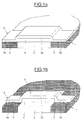
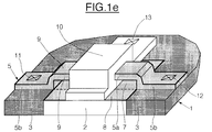
- FIGS. 1a to 1e schematic representations of main steps in carrying out the method of the invention.
- the process of the invention begins, as shown in Figure la, by deposition by selective epitaxy on a main surface of a active central region 2 in silicon of a substrate 1 of a layer 4 of a Monocrystalline SiGe alloy over a thickness between 1 and 50 nm.
- the active central region 2 of the substrate 1 is surrounded by a region insulating device 3.
- the SiGe alloy layer as well as the main surface of the insulating peripheral region, are covered by non-selective epitaxy of a silicon layer 5 thus forming a bridge-like structure very thin between 1 and 50 nm and preferably between 1 and 20 nm.
- Layer 5 of silicon is monocrystalline in its part central 5a of the active zone (this part will form the channel of transistor), and polycrystalline in its parts 5b which rest on the insulation (these parts will form the source and drain regions of the device).
- This silicon layer is then doped by masking and ion implantation in a conventional manner in the area which, thereafter, will constitute the transistor channel.
- the height of the tunnel 7 corresponds to the thickness of layer 4 and is therefore between 1 and 50 nm.
- thermal oxidation we form, for example by thermal oxidation, a thin layer 8 of silicon oxide on the main surface of the active central region 2 and the internal surface of the tunnel 7, avoiding filling tunnel 7.
- thermal oxidation also leads to the covering of the surface external and flanks of the bridge structure by a layer of oxide of silicon 9.
- a layer of silicon is then deposited in a conventional manner polycrystalline so as to cover the entire main surface of the substrate 1 and fill the tunnel 7.
- This layer of polycrystalline silicon is preferably doped in situ in a conventional manner.
- the layer of polycrystalline silicon using photo lithography techniques classics to form the GAA 10 architecture grid.
- the source and drain regions by ion implantation and we equip them, as well as the grid region of the contacts, notes: 11 for the source, 12 for the drain and 13 for the grid.
- the semiconductor device such as a transistor, is then completed in a conventional manner.
Landscapes
- Insulated Gate Type Field-Effect Transistor (AREA)
Abstract
Description
Claims (12)
- Procédé de fabrication d'un dispositif semi-conducteur d'architecture à grille enveloppante, caractérisé en ce qu'il comprend les étapes suivantes :(a) obtention d'un substrat comprenant une région centrale active (2) en matériau semi-conducteur entourée par une région périphérique isolante (3) en matériau diélectrique, lesdites régions comportant respectivement une surface principale active et une surface principale isolante coextensives constituant une surface principale du substrat ;(b) par épitaxie sélective d'une couche de Ge ou d'un alliage SiGe moncristallin (4) sur la surface principale active ;(c) formation par épitaxie non sélective sur la couche de Ge ou d'alliage SiGe monocristallin et sur la surface principale isolante d'une couche de silicium (5) qui est monocristalline dans sa partie reposant sur la couche Ge ou d'alliage SiGe monocristallin, et qui est polycristalline dans ses parties reposant sur la surface isolante ;(d) masquage et gravure de la couche de silicium (5) et de la couche de Ge ou d'alliage SiGe (4) pour former sur la surface principale active un empilement (6) ayant deux flancs opposés laissant apparaítre la couche de Ge ou d'alliage SiGe monocristallin ;(e) élimination par gravure sélective de la couche de Ge ou d'alliage SiGe monocristallin, de sorte que la couche de silicium de l'empilement forme une structure en pont sur la surface principale active, ladite structure en pont comportant des flancs, une surface externe et une surface interne définissant avec une partie correspondante de la surface principale active un tunnel (7) ;(f) formation sur les surfaces externe et interne de la structure en pont ainsi que sur ses flancs d'une mince couche d'un matériau diélectrique (8, 9) ne comblant pas le tunnel ;(g) dépôt d'un matériau conducteur de manière à recouvrir la structure en pont et à remplir le tunnel ; et(h) le masquage et la gravure du matériau conducteur pour former une région de grille (10) d'architecture enveloppante, de dimension et géométrie voulues.
- Procédé selon la revendication 1, caractérisé en ce qu'il comprend avant l'étape (d) une étape de dopage de la couche de silicium (5).
- Procédé selon la revendication 2, caractérisé en ce que le dopage s'effectue in situ lors du dépôt de la couche de silicium (5).
- Procédé selon la revendication 2, caractérisé en ce que le dopage s'effectue par l'implantation ionique après formation de la couche de silicium (5).
- Procédé selon l'une quelconque des revendications 1 à 4, caractérisé en ce que la région centrale active (2) du substrat (1) est en silicium.
- Procédé selon l'une quelconque des revendications précédentes, caractérisé en ce que le matériau conducteur de l'étape (g) est un métal ou du silicium polycristallin.
- Procédé selon l'une quelconque des revendications précédentes, caractérisé en ce que le dispositif semi-conducteur est un transistor.
- Dispositif semi-conducteur comprenant un substrat (1) ayant une région centrale active (2) en matériau semi-conducteur entourée d'une région périphérique isolante (3) en matériau diélectrique, lesdites régions ayant respectivement une surface principale active et une surface principale isolante coextensive constituant une surface principale du substrat, ladite surface principale du substrat présentant une structure en pont (5) constituée de silicium et ayant deux parties latérales opposées en silicium polycristallin (5b) reposant sur des parties opposées de la région périphérique isolante constituant des régions de source et de drain et réunies par une partie centrale (5a) espacée au-dessus de ladite région active du substrat constituant une région de canal du dispositif, une région de grille (10) entourant la partie centrale de la structure en pont caractérisé en ce que ladite partie centrale (5a) est en silicium monocristallin et présente une épaisseur comprise entre 1 à 50 nm.
- Dispositif selon la revendication 8, caractérisé en ce que l'épaisseur de la partie centrale varie de 1 à 20 nm.
- Dispositif selon la revendication 8, caractérisé en ce que la partie centrale est espacée de la surface principale de la région centrale active du substrat d'une hauteur de 1 à 50 nm.
- Dispositif selon l'une quelconque des revendications 8 à 10, caractérisé en ce que des contacts de source et de drain sont disposés sur les parties latérales en silicium polycristallin de la structure en pont au-dessus de la région périphérique isolante.
- Dispositif selon l'une quelconque des revendications 8 à 11, caractérisé en ce que le dispositif est un transistor.
Applications Claiming Priority (2)
| Application Number | Priority Date | Filing Date | Title |
|---|---|---|---|
| FR9912406A FR2799305B1 (fr) | 1999-10-05 | 1999-10-05 | Procede de fabrication d'un dispositif semi-conducteur a grille enveloppante et dispositif obtenu |
| FR9912406 | 1999-10-05 |
Publications (1)
| Publication Number | Publication Date |
|---|---|
| EP1091417A1 true EP1091417A1 (fr) | 2001-04-11 |
Family
ID=9550587
Family Applications (1)
| Application Number | Title | Priority Date | Filing Date |
|---|---|---|---|
| EP00402754A Withdrawn EP1091417A1 (fr) | 1999-10-05 | 2000-10-05 | Procédé fabrication d'un dispositif semi-conducteur à grille enveloppante et dispositif obtenu |
Country Status (3)
| Country | Link |
|---|---|
| US (1) | US6495403B1 (fr) |
| EP (1) | EP1091417A1 (fr) |
| FR (1) | FR2799305B1 (fr) |
Cited By (5)
| Publication number | Priority date | Publication date | Assignee | Title |
|---|---|---|---|---|
| FR2845201A1 (fr) * | 2002-09-27 | 2004-04-02 | St Microelectronics Sa | Procede de formation de portions d'un materiau compose a l'interieur d'une cavite et circuit electrique incorporant des portions de materiau compose ainsi obtenues |
| FR2860099A1 (fr) * | 2003-09-18 | 2005-03-25 | St Microelectronics Sa | Procede de realisation d'un transistor a effet de champ et transistor ainsi obtenu |
| US6940129B2 (en) * | 2003-01-20 | 2005-09-06 | Samsung Electronics Co., Ltd. | Double gate MOS transistors |
| EP1436843A4 (fr) * | 2001-09-21 | 2008-11-26 | Ibm | Procede pour transistor a effet de champ mos a grille enroulee |
| EP1507286B1 (fr) * | 2003-08-12 | 2015-12-09 | Commissariat à l'Énergie Atomique et aux Énergies Alternatives | Procédé de formation d'un réseau d'interconnexions d'un circuit intégré et procédé de formation d'un transistor à grille entourante |
Families Citing this family (44)
| Publication number | Priority date | Publication date | Assignee | Title |
|---|---|---|---|---|
| FR2795555B1 (fr) * | 1999-06-28 | 2002-12-13 | France Telecom | Procede de fabrication d'un dispositif semi-conducteur comprenant un empilement forme alternativement de couches de silicium et de couches de materiau dielectrique |
| KR100414217B1 (ko) * | 2001-04-12 | 2004-01-07 | 삼성전자주식회사 | 게이트 올 어라운드형 트랜지스터를 가진 반도체 장치 및그 형성 방법 |
| FR2838238B1 (fr) * | 2002-04-08 | 2005-04-15 | St Microelectronics Sa | Dispositif semiconducteur a grille enveloppante encapsule dans un milieu isolant |
| FR2853454B1 (fr) * | 2003-04-03 | 2005-07-15 | St Microelectronics Sa | Transistor mos haute densite |
| US6894326B2 (en) * | 2003-06-25 | 2005-05-17 | International Business Machines Corporation | High-density finFET integration scheme |
| US7456476B2 (en) | 2003-06-27 | 2008-11-25 | Intel Corporation | Nonplanar semiconductor device with partially or fully wrapped around gate electrode and methods of fabrication |
| US6909151B2 (en) | 2003-06-27 | 2005-06-21 | Intel Corporation | Nonplanar device with stress incorporation layer and method of fabrication |
| FR2857952B1 (fr) | 2003-07-25 | 2005-12-16 | St Microelectronics Sa | Resonateur electromecanique et procede de fabrication d'un tel resonateur |
| KR100526887B1 (ko) * | 2004-02-10 | 2005-11-09 | 삼성전자주식회사 | 전계효과 트랜지스터 및 그의 제조방법 |
| KR100598099B1 (ko) * | 2004-02-24 | 2006-07-07 | 삼성전자주식회사 | 다마신 게이트를 갖는 수직 채널 핀 전계효과 트랜지스터 및 그 제조방법 |
| US7154118B2 (en) | 2004-03-31 | 2006-12-26 | Intel Corporation | Bulk non-planar transistor having strained enhanced mobility and methods of fabrication |
| KR100612415B1 (ko) * | 2004-04-09 | 2006-08-16 | 삼성전자주식회사 | 올 어라운드된 채널 영역을 갖는 트랜지스터 및 그 제조방법 |
| KR100532564B1 (ko) * | 2004-05-25 | 2005-12-01 | 한국전자통신연구원 | 다중 게이트 모스 트랜지스터 및 그 제조 방법 |
| DE102005026228B4 (de) * | 2004-06-08 | 2010-04-15 | Samsung Electronics Co., Ltd., Suwon | Transistor vom GAA-Typ und Verfahren zu dessen Herstellung |
| KR100618831B1 (ko) * | 2004-06-08 | 2006-09-08 | 삼성전자주식회사 | 게이트 올 어라운드형 반도체소자 및 그 제조방법 |
| US7042009B2 (en) | 2004-06-30 | 2006-05-09 | Intel Corporation | High mobility tri-gate devices and methods of fabrication |
| US7348284B2 (en) | 2004-08-10 | 2008-03-25 | Intel Corporation | Non-planar pMOS structure with a strained channel region and an integrated strained CMOS flow |
| US7332439B2 (en) | 2004-09-29 | 2008-02-19 | Intel Corporation | Metal gate transistors with epitaxial source and drain regions |
| US7422946B2 (en) | 2004-09-29 | 2008-09-09 | Intel Corporation | Independently accessed double-gate and tri-gate transistors in same process flow |
| US20060086977A1 (en) | 2004-10-25 | 2006-04-27 | Uday Shah | Nonplanar device with thinned lower body portion and method of fabrication |
| US7202117B2 (en) * | 2005-01-31 | 2007-04-10 | Freescale Semiconductor, Inc. | Method of making a planar double-gated transistor |
| FR2881877B1 (fr) * | 2005-02-04 | 2007-08-31 | Soitec Silicon On Insulator | Transistor a effet de champ multi-grille a canal multi-couche |
| US7518196B2 (en) | 2005-02-23 | 2009-04-14 | Intel Corporation | Field effect transistor with narrow bandgap source and drain regions and method of fabrication |
| US20060202266A1 (en) | 2005-03-14 | 2006-09-14 | Marko Radosavljevic | Field effect transistor with metal source/drain regions |
| KR100594327B1 (ko) * | 2005-03-24 | 2006-06-30 | 삼성전자주식회사 | 라운드 형태의 단면을 가지는 나노와이어를 구비한 반도체소자 및 그 제조 방법 |
| US7858481B2 (en) | 2005-06-15 | 2010-12-28 | Intel Corporation | Method for fabricating transistor with thinned channel |
| US7547637B2 (en) | 2005-06-21 | 2009-06-16 | Intel Corporation | Methods for patterning a semiconductor film |
| US7279375B2 (en) | 2005-06-30 | 2007-10-09 | Intel Corporation | Block contact architectures for nanoscale channel transistors |
| US7402875B2 (en) | 2005-08-17 | 2008-07-22 | Intel Corporation | Lateral undercut of metal gate in SOI device |
| KR100696197B1 (ko) * | 2005-09-27 | 2007-03-20 | 한국전자통신연구원 | 실리콘 기판을 이용한 다중 게이트 모스 트랜지스터 및 그제조 방법 |
| US7479421B2 (en) | 2005-09-28 | 2009-01-20 | Intel Corporation | Process for integrating planar and non-planar CMOS transistors on a bulk substrate and article made thereby |
| US20070090416A1 (en) | 2005-09-28 | 2007-04-26 | Doyle Brian S | CMOS devices with a single work function gate electrode and method of fabrication |
| US7485503B2 (en) | 2005-11-30 | 2009-02-03 | Intel Corporation | Dielectric interface for group III-V semiconductor device |
| FR2883661B1 (fr) * | 2006-05-04 | 2008-04-25 | Soitec Silicon On Insulator | Transistor a effet de champ multi-grille a canal multi-couche |
| US8143646B2 (en) | 2006-08-02 | 2012-03-27 | Intel Corporation | Stacking fault and twin blocking barrier for integrating III-V on Si |
| FR2906238B1 (fr) * | 2006-09-27 | 2008-12-19 | Commissariat Energie Atomique | Procede de realisation d'un composant electromecanique sur un substrat plan |
| FR2921751B1 (fr) * | 2007-10-02 | 2009-12-18 | St Microelectronics Crolles 2 | Procede de realisation de dispositif semi-conducteur a architecture asymetrique |
| CN101556922B (zh) * | 2008-04-10 | 2010-07-28 | 北京大学 | 一种纳米环栅mosfet晶体管及其制备方法 |
| US8362566B2 (en) | 2008-06-23 | 2013-01-29 | Intel Corporation | Stress in trigate devices using complimentary gate fill materials |
| JP6050034B2 (ja) * | 2012-06-12 | 2016-12-21 | 猛英 白土 | 半導体装置及びその製造方法 |
| US8975674B2 (en) | 2012-11-09 | 2015-03-10 | National Applied Research Laboratories | Bridge structure |
| US8815691B2 (en) | 2012-12-21 | 2014-08-26 | Taiwan Semiconductor Manufacturing Company, Ltd. | Method of fabricating a gate all around device |
| US9281379B1 (en) | 2014-11-19 | 2016-03-08 | International Business Machines Corporation | Gate-all-around fin device |
| US10170304B1 (en) | 2017-10-25 | 2019-01-01 | Globalfoundries Inc. | Self-aligned nanotube structures |
Citations (4)
| Publication number | Priority date | Publication date | Assignee | Title |
|---|---|---|---|---|
| US5188973A (en) * | 1991-05-09 | 1993-02-23 | Nippon Telegraph & Telephone Corporation | Method of manufacturing SOI semiconductor element |
| US5578513A (en) * | 1993-09-17 | 1996-11-26 | Mitsubishi Denki Kabushiki Kaisha | Method of making a semiconductor device having a gate all around type of thin film transistor |
| US5801397A (en) * | 1994-09-30 | 1998-09-01 | Sgs-Thomson Microelectronics, Inc. | Device having a self-aligned gate electrode wrapped around the channel |
| DE19803479A1 (de) * | 1997-06-18 | 1998-12-24 | Mitsubishi Electric Corp | Halbleitereinrichtung und Herstellungsverfahren einer Halbleitereinrichtung |
-
1999
- 1999-10-05 FR FR9912406A patent/FR2799305B1/fr not_active Expired - Fee Related
-
2000
- 2000-10-05 US US09/680,035 patent/US6495403B1/en not_active Expired - Lifetime
- 2000-10-05 EP EP00402754A patent/EP1091417A1/fr not_active Withdrawn
Patent Citations (5)
| Publication number | Priority date | Publication date | Assignee | Title |
|---|---|---|---|---|
| US5188973A (en) * | 1991-05-09 | 1993-02-23 | Nippon Telegraph & Telephone Corporation | Method of manufacturing SOI semiconductor element |
| US5578513A (en) * | 1993-09-17 | 1996-11-26 | Mitsubishi Denki Kabushiki Kaisha | Method of making a semiconductor device having a gate all around type of thin film transistor |
| US5583362A (en) * | 1993-09-17 | 1996-12-10 | Mitsubishi Denki Kabushiki Kaisha | Gate all around thin film transistor |
| US5801397A (en) * | 1994-09-30 | 1998-09-01 | Sgs-Thomson Microelectronics, Inc. | Device having a self-aligned gate electrode wrapped around the channel |
| DE19803479A1 (de) * | 1997-06-18 | 1998-12-24 | Mitsubishi Electric Corp | Halbleitereinrichtung und Herstellungsverfahren einer Halbleitereinrichtung |
Cited By (7)
| Publication number | Priority date | Publication date | Assignee | Title |
|---|---|---|---|---|
| EP1436843A4 (fr) * | 2001-09-21 | 2008-11-26 | Ibm | Procede pour transistor a effet de champ mos a grille enroulee |
| FR2845201A1 (fr) * | 2002-09-27 | 2004-04-02 | St Microelectronics Sa | Procede de formation de portions d'un materiau compose a l'interieur d'une cavite et circuit electrique incorporant des portions de materiau compose ainsi obtenues |
| US7188411B2 (en) | 2002-09-27 | 2007-03-13 | Stmicroelectronics S.A. | Process for forming portions of a compound material inside a cavity |
| US6940129B2 (en) * | 2003-01-20 | 2005-09-06 | Samsung Electronics Co., Ltd. | Double gate MOS transistors |
| EP1507286B1 (fr) * | 2003-08-12 | 2015-12-09 | Commissariat à l'Énergie Atomique et aux Énergies Alternatives | Procédé de formation d'un réseau d'interconnexions d'un circuit intégré et procédé de formation d'un transistor à grille entourante |
| FR2860099A1 (fr) * | 2003-09-18 | 2005-03-25 | St Microelectronics Sa | Procede de realisation d'un transistor a effet de champ et transistor ainsi obtenu |
| US7297578B2 (en) | 2003-09-18 | 2007-11-20 | Stmicroelectronics S.A. | Method for producing a field effect transistor |
Also Published As
| Publication number | Publication date |
|---|---|
| FR2799305B1 (fr) | 2004-06-18 |
| FR2799305A1 (fr) | 2001-04-06 |
| US6495403B1 (en) | 2002-12-17 |
Similar Documents
| Publication | Publication Date | Title |
|---|---|---|
| FR2799305A1 (fr) | Procede de fabrication d'un dispositif semi-conducteur a grille enveloppante et dispositif obtenu | |
| EP1837916B1 (fr) | Procédé de réalisation d'un transistor à canal comprenant du germanium | |
| EP1266409B1 (fr) | Transistor mos a source et drain metalliques, et procede de fabrication d'un tel transistor | |
| FR3060840A1 (fr) | Procede de realisation d'un dispositif semi-conducteur a espaceurs internes auto-alignes | |
| FR2823009A1 (fr) | Procede de fabrication d'un transistor vertical a grille isolee a faible recouvrement de la grille sur la source et sur le drain, et circuit integre comportant un tel transistor | |
| FR2823010A1 (fr) | Procede de fabrication d'un transistor vertical a grille isolee a quadruple canal de conduction, et circuit integre comportant un tel transistor | |
| FR2838238A1 (fr) | Dispositif semiconducteur a grille enveloppante encapsule dans un milieu isolant | |
| FR2795554A1 (fr) | Procede de gravure laterale par trous pour fabriquer des dis positifs semi-conducteurs | |
| EP0635880B1 (fr) | Procédé de fabrication d'un transistor en technologie silicium sur isolant | |
| EP1132955A1 (fr) | Procédé de fabrication d'un transistor bipolaire double-polysilicium autoaligné. | |
| EP1589572B1 (fr) | Procédé de fabrication d'un circuit intégré comprenant l'élaboration de tranchées d'isolation creuses | |
| EP3503175A1 (fr) | Procede de realisation d'un substrat semi-conducteur comprenant au moins une portion de semi-conducteur contraint en compression | |
| FR2799307A1 (fr) | Dispositif semi-conducteur combinant les avantages des architectures massives et soi, procede de fabrication | |
| EP1788635B1 (fr) | Procédé de réalisation de transistor à double grilles auto-alignées par réduction de motifs de grille | |
| EP3671826B1 (fr) | Procédé amélioré de fabrication d'un circuit intégré comportant un transistor nmos et un transistor pmos | |
| EP4006996B1 (fr) | Dispositif quantique et procédé de réalisation | |
| EP1166362A1 (fr) | Nouveau dispositif semi-conducteur combinant les avantages des architectures massive et soi, et procede de fabrication | |
| EP1407486B1 (fr) | Procede de fabrication d'un transistor sur un substrat soi | |
| FR2887370A1 (fr) | Procede de fabrication d'un transistor isole a canal contraint | |
| EP3961721A1 (fr) | Procede ameliore d'enrichissement germanium autour du canal d'un transistor | |
| EP0403368A1 (fr) | Procédé de fabrication d'un circuit integré comportant un transistor à effet de champ à double implantation | |
| EP4002482B1 (fr) | Procédé de fabrication d'une zone dopée d'un dispositif microélectronique | |
| EP3035386B1 (fr) | Procédé de réalisation d'un dispositif à effet de champ amélioré | |
| EP3961720B1 (fr) | Enrichissement germanium autour du canal par blocs sureleves | |
| EP4006997B1 (fr) | Procédé de réalisation d'un dispositif quantique |
Legal Events
| Date | Code | Title | Description |
|---|---|---|---|
| PUAI | Public reference made under article 153(3) epc to a published international application that has entered the european phase |
Free format text: ORIGINAL CODE: 0009012 |
|
| AK | Designated contracting states |
Kind code of ref document: A1 Designated state(s): DE FR GB IT |
|
| AX | Request for extension of the european patent |
Free format text: AL;LT;LV;MK;RO;SI |
|
| 17P | Request for examination filed |
Effective date: 20011011 |
|
| RAP1 | Party data changed (applicant data changed or rights of an application transferred) |
Owner name: STMICROELECTRONICS S.A. |
|
| AKX | Designation fees paid |
Free format text: DE FR GB IT |
|
| 17Q | First examination report despatched |
Effective date: 20060911 |
|
| STAA | Information on the status of an ep patent application or granted ep patent |
Free format text: STATUS: THE APPLICATION IS DEEMED TO BE WITHDRAWN |
|
| 18D | Application deemed to be withdrawn |
Effective date: 20070323 |