EP1082884B1 - Verfahren zur herstellung von verdrahtungen mit lothöckern - Google Patents
Verfahren zur herstellung von verdrahtungen mit lothöckern Download PDFInfo
- Publication number
- EP1082884B1 EP1082884B1 EP99927832A EP99927832A EP1082884B1 EP 1082884 B1 EP1082884 B1 EP 1082884B1 EP 99927832 A EP99927832 A EP 99927832A EP 99927832 A EP99927832 A EP 99927832A EP 1082884 B1 EP1082884 B1 EP 1082884B1
- Authority
- EP
- European Patent Office
- Prior art keywords
- solder
- conductor
- connection pads
- reduced width
- width
- Prior art date
- Legal status (The legal status is an assumption and is not a legal conclusion. Google has not performed a legal analysis and makes no representation as to the accuracy of the status listed.)
- Expired - Lifetime
Links
Images


Classifications
-
- H—ELECTRICITY
- H10—SEMICONDUCTOR DEVICES; ELECTRIC SOLID-STATE DEVICES NOT OTHERWISE PROVIDED FOR
- H10W—GENERIC PACKAGES, INTERCONNECTIONS, CONNECTORS OR OTHER CONSTRUCTIONAL DETAILS OF DEVICES COVERED BY CLASS H10
- H10W70/00—Package substrates; Interposers; Redistribution layers [RDL]
- H10W70/01—Manufacture or treatment
- H10W70/05—Manufacture or treatment of insulating or insulated package substrates, or of interposers, or of redistribution layers
- H10W70/093—Connecting or disconnecting other interconnections thereto or therefrom, e.g. connecting bond wires or bumps
-
- H—ELECTRICITY
- H05—ELECTRIC TECHNIQUES NOT OTHERWISE PROVIDED FOR
- H05K—PRINTED CIRCUITS; CASINGS OR CONSTRUCTIONAL DETAILS OF ELECTRIC APPARATUS; MANUFACTURE OF ASSEMBLAGES OF ELECTRICAL COMPONENTS
- H05K3/00—Apparatus or processes for manufacturing printed circuits
- H05K3/30—Assembling printed circuits with electric components, e.g. with resistors
- H05K3/32—Assembling printed circuits with electric components, e.g. with resistors electrically connecting electric components or wires to printed circuits
- H05K3/34—Assembling printed circuits with electric components, e.g. with resistors electrically connecting electric components or wires to printed circuits by soldering
-
- H—ELECTRICITY
- H05—ELECTRIC TECHNIQUES NOT OTHERWISE PROVIDED FOR
- H05K—PRINTED CIRCUITS; CASINGS OR CONSTRUCTIONAL DETAILS OF ELECTRIC APPARATUS; MANUFACTURE OF ASSEMBLAGES OF ELECTRICAL COMPONENTS
- H05K1/00—Printed circuits
- H05K1/02—Details
- H05K1/11—Printed elements for providing electric connections to or between printed circuits
- H05K1/111—Pads for surface mounting, e.g. lay-out
-
- H—ELECTRICITY
- H05—ELECTRIC TECHNIQUES NOT OTHERWISE PROVIDED FOR
- H05K—PRINTED CIRCUITS; CASINGS OR CONSTRUCTIONAL DETAILS OF ELECTRIC APPARATUS; MANUFACTURE OF ASSEMBLAGES OF ELECTRICAL COMPONENTS
- H05K3/00—Apparatus or processes for manufacturing printed circuits
- H05K3/30—Assembling printed circuits with electric components, e.g. with resistors
- H05K3/32—Assembling printed circuits with electric components, e.g. with resistors electrically connecting electric components or wires to printed circuits
- H05K3/34—Assembling printed circuits with electric components, e.g. with resistors electrically connecting electric components or wires to printed circuits by soldering
- H05K3/3465—Application of solder
- H05K3/3473—Plating of solder
-
- H—ELECTRICITY
- H10—SEMICONDUCTOR DEVICES; ELECTRIC SOLID-STATE DEVICES NOT OTHERWISE PROVIDED FOR
- H10W—GENERIC PACKAGES, INTERCONNECTIONS, CONNECTORS OR OTHER CONSTRUCTIONAL DETAILS OF DEVICES COVERED BY CLASS H10
- H10W72/00—Interconnections or connectors in packages
- H10W72/01—Manufacture or treatment
- H10W72/012—Manufacture or treatment of bump connectors, dummy bumps or thermal bumps
-
- H—ELECTRICITY
- H05—ELECTRIC TECHNIQUES NOT OTHERWISE PROVIDED FOR
- H05K—PRINTED CIRCUITS; CASINGS OR CONSTRUCTIONAL DETAILS OF ELECTRIC APPARATUS; MANUFACTURE OF ASSEMBLAGES OF ELECTRICAL COMPONENTS
- H05K2201/00—Indexing scheme relating to printed circuits covered by H05K1/00
- H05K2201/09—Shape and layout
- H05K2201/09209—Shape and layout details of conductors
- H05K2201/09372—Pads and lands
- H05K2201/09381—Shape of non-curved single flat metallic pad, land or exposed part thereof; Shape of electrode of leadless component
-
- H—ELECTRICITY
- H05—ELECTRIC TECHNIQUES NOT OTHERWISE PROVIDED FOR
- H05K—PRINTED CIRCUITS; CASINGS OR CONSTRUCTIONAL DETAILS OF ELECTRIC APPARATUS; MANUFACTURE OF ASSEMBLAGES OF ELECTRICAL COMPONENTS
- H05K2201/00—Indexing scheme relating to printed circuits covered by H05K1/00
- H05K2201/09—Shape and layout
- H05K2201/09209—Shape and layout details of conductors
- H05K2201/09654—Shape and layout details of conductors covering at least two types of conductors provided for in H05K2201/09218 - H05K2201/095
- H05K2201/09727—Varying width along a single conductor; Conductors or pads having different widths
-
- H—ELECTRICITY
- H05—ELECTRIC TECHNIQUES NOT OTHERWISE PROVIDED FOR
- H05K—PRINTED CIRCUITS; CASINGS OR CONSTRUCTIONAL DETAILS OF ELECTRIC APPARATUS; MANUFACTURE OF ASSEMBLAGES OF ELECTRICAL COMPONENTS
- H05K2201/00—Indexing scheme relating to printed circuits covered by H05K1/00
- H05K2201/10—Details of components or other objects attached to or integrated in a printed circuit board
- H05K2201/10613—Details of electrical connections of non-printed components, e.g. special leads
- H05K2201/10621—Components characterised by their electrical contacts
- H05K2201/10674—Flip chip
-
- H—ELECTRICITY
- H05—ELECTRIC TECHNIQUES NOT OTHERWISE PROVIDED FOR
- H05K—PRINTED CIRCUITS; CASINGS OR CONSTRUCTIONAL DETAILS OF ELECTRIC APPARATUS; MANUFACTURE OF ASSEMBLAGES OF ELECTRICAL COMPONENTS
- H05K2203/00—Indexing scheme relating to apparatus or processes for manufacturing printed circuits covered by H05K3/00
- H05K2203/04—Soldering or other types of metallurgic bonding
- H05K2203/042—Remote solder depot on the PCB, the solder flowing to the connections from this depot
-
- H—ELECTRICITY
- H05—ELECTRIC TECHNIQUES NOT OTHERWISE PROVIDED FOR
- H05K—PRINTED CIRCUITS; CASINGS OR CONSTRUCTIONAL DETAILS OF ELECTRIC APPARATUS; MANUFACTURE OF ASSEMBLAGES OF ELECTRICAL COMPONENTS
- H05K2203/00—Indexing scheme relating to apparatus or processes for manufacturing printed circuits covered by H05K3/00
- H05K2203/04—Soldering or other types of metallurgic bonding
- H05K2203/043—Reflowing of solder coated conductors, not during connection of components, e.g. reflowing solder paste
-
- H—ELECTRICITY
- H05—ELECTRIC TECHNIQUES NOT OTHERWISE PROVIDED FOR
- H05K—PRINTED CIRCUITS; CASINGS OR CONSTRUCTIONAL DETAILS OF ELECTRIC APPARATUS; MANUFACTURE OF ASSEMBLAGES OF ELECTRICAL COMPONENTS
- H05K2203/00—Indexing scheme relating to apparatus or processes for manufacturing printed circuits covered by H05K3/00
- H05K2203/10—Using electric, magnetic and electromagnetic fields; Using laser light
- H05K2203/107—Using laser light
-
- H—ELECTRICITY
- H05—ELECTRIC TECHNIQUES NOT OTHERWISE PROVIDED FOR
- H05K—PRINTED CIRCUITS; CASINGS OR CONSTRUCTIONAL DETAILS OF ELECTRIC APPARATUS; MANUFACTURE OF ASSEMBLAGES OF ELECTRICAL COMPONENTS
- H05K3/00—Apparatus or processes for manufacturing printed circuits
- H05K3/02—Apparatus or processes for manufacturing printed circuits in which the conductive material is applied to the surface of the insulating support and is thereafter removed from such areas of the surface which are not intended for current conducting or shielding
- H05K3/06—Apparatus or processes for manufacturing printed circuits in which the conductive material is applied to the surface of the insulating support and is thereafter removed from such areas of the surface which are not intended for current conducting or shielding the conductive material being removed chemically or electrolytically, e.g. by photo-etch process
- H05K3/061—Etching masks
- H05K3/062—Etching masks consisting of metals or alloys or metallic inorganic compounds
-
- H—ELECTRICITY
- H05—ELECTRIC TECHNIQUES NOT OTHERWISE PROVIDED FOR
- H05K—PRINTED CIRCUITS; CASINGS OR CONSTRUCTIONAL DETAILS OF ELECTRIC APPARATUS; MANUFACTURE OF ASSEMBLAGES OF ELECTRICAL COMPONENTS
- H05K3/00—Apparatus or processes for manufacturing printed circuits
- H05K3/22—Secondary treatment of printed circuits
- H05K3/24—Reinforcing of the conductive pattern
- H05K3/241—Reinforcing of the conductive pattern characterised by the electroplating method; means therefor, e.g. baths or apparatus
- H05K3/242—Reinforcing of the conductive pattern characterised by the electroplating method; means therefor, e.g. baths or apparatus characterised by using temporary conductors on the printed circuit for electrically connecting areas which are to be electroplated
-
- H—ELECTRICITY
- H05—ELECTRIC TECHNIQUES NOT OTHERWISE PROVIDED FOR
- H05K—PRINTED CIRCUITS; CASINGS OR CONSTRUCTIONAL DETAILS OF ELECTRIC APPARATUS; MANUFACTURE OF ASSEMBLAGES OF ELECTRICAL COMPONENTS
- H05K3/00—Apparatus or processes for manufacturing printed circuits
- H05K3/30—Assembling printed circuits with electric components, e.g. with resistors
- H05K3/32—Assembling printed circuits with electric components, e.g. with resistors electrically connecting electric components or wires to printed circuits
- H05K3/34—Assembling printed circuits with electric components, e.g. with resistors electrically connecting electric components or wires to printed circuits by soldering
- H05K3/3494—Heating processes for reflow soldering
-
- H—ELECTRICITY
- H10—SEMICONDUCTOR DEVICES; ELECTRIC SOLID-STATE DEVICES NOT OTHERWISE PROVIDED FOR
- H10W—GENERIC PACKAGES, INTERCONNECTIONS, CONNECTORS OR OTHER CONSTRUCTIONAL DETAILS OF DEVICES COVERED BY CLASS H10
- H10W72/00—Interconnections or connectors in packages
- H10W72/071—Connecting or disconnecting
- H10W72/072—Connecting or disconnecting of bump connectors
-
- H—ELECTRICITY
- H10—SEMICONDUCTOR DEVICES; ELECTRIC SOLID-STATE DEVICES NOT OTHERWISE PROVIDED FOR
- H10W—GENERIC PACKAGES, INTERCONNECTIONS, CONNECTORS OR OTHER CONSTRUCTIONAL DETAILS OF DEVICES COVERED BY CLASS H10
- H10W72/00—Interconnections or connectors in packages
- H10W72/071—Connecting or disconnecting
- H10W72/072—Connecting or disconnecting of bump connectors
- H10W72/07231—Techniques
- H10W72/07236—Soldering or alloying
-
- H—ELECTRICITY
- H10—SEMICONDUCTOR DEVICES; ELECTRIC SOLID-STATE DEVICES NOT OTHERWISE PROVIDED FOR
- H10W—GENERIC PACKAGES, INTERCONNECTIONS, CONNECTORS OR OTHER CONSTRUCTIONAL DETAILS OF DEVICES COVERED BY CLASS H10
- H10W72/00—Interconnections or connectors in packages
- H10W72/20—Bump connectors, e.g. solder bumps or copper pillars; Dummy bumps; Thermal bumps
- H10W72/241—Dispositions, e.g. layouts
-
- H—ELECTRICITY
- H10—SEMICONDUCTOR DEVICES; ELECTRIC SOLID-STATE DEVICES NOT OTHERWISE PROVIDED FOR
- H10W—GENERIC PACKAGES, INTERCONNECTIONS, CONNECTORS OR OTHER CONSTRUCTIONAL DETAILS OF DEVICES COVERED BY CLASS H10
- H10W72/00—Interconnections or connectors in packages
- H10W72/20—Bump connectors, e.g. solder bumps or copper pillars; Dummy bumps; Thermal bumps
- H10W72/251—Materials
-
- H—ELECTRICITY
- H10—SEMICONDUCTOR DEVICES; ELECTRIC SOLID-STATE DEVICES NOT OTHERWISE PROVIDED FOR
- H10W—GENERIC PACKAGES, INTERCONNECTIONS, CONNECTORS OR OTHER CONSTRUCTIONAL DETAILS OF DEVICES COVERED BY CLASS H10
- H10W72/00—Interconnections or connectors in packages
- H10W72/90—Bond pads, in general
- H10W72/921—Structures or relative sizes of bond pads
- H10W72/923—Bond pads having multiple stacked layers
-
- H—ELECTRICITY
- H10—SEMICONDUCTOR DEVICES; ELECTRIC SOLID-STATE DEVICES NOT OTHERWISE PROVIDED FOR
- H10W—GENERIC PACKAGES, INTERCONNECTIONS, CONNECTORS OR OTHER CONSTRUCTIONAL DETAILS OF DEVICES COVERED BY CLASS H10
- H10W72/00—Interconnections or connectors in packages
- H10W72/90—Bond pads, in general
- H10W72/951—Materials of bond pads
- H10W72/952—Materials of bond pads comprising metals or metalloids, e.g. PbSn, Ag or Cu
-
- Y—GENERAL TAGGING OF NEW TECHNOLOGICAL DEVELOPMENTS; GENERAL TAGGING OF CROSS-SECTIONAL TECHNOLOGIES SPANNING OVER SEVERAL SECTIONS OF THE IPC; TECHNICAL SUBJECTS COVERED BY FORMER USPC CROSS-REFERENCE ART COLLECTIONS [XRACs] AND DIGESTS
- Y02—TECHNOLOGIES OR APPLICATIONS FOR MITIGATION OR ADAPTATION AGAINST CLIMATE CHANGE
- Y02P—CLIMATE CHANGE MITIGATION TECHNOLOGIES IN THE PRODUCTION OR PROCESSING OF GOODS
- Y02P70/00—Climate change mitigation technologies in the production process for final industrial or consumer products
- Y02P70/50—Manufacturing or production processes characterised by the final manufactured product
Definitions
- Integrated circuits are getting more and more connections and are miniaturized more and more.
- the one at this increasing miniaturization expected difficulties with Solder paste application and assembly should be done with new housing shapes be remedied, whereby in particular single, Few or to highlight multi-chip modules in the Ball Grid Array Package are (DE-Z productronic 5, 1994, pages 54,55).
- These modules are based on a plated-through substrate on which the chips, for example, via contact wires or by means of Flipchip assembly are contacted.
- the Ball Grid Array BGA
- the ball grid array encompasses the underside of the substrate surface-mounted solder bumps that surface mount enable on the printed circuit boards or assemblies. Due to the flat arrangement of the solder bumps, high Connection numbers in a rough grid, for example 1.27 mm can be realized.
- DE-C-195 35 622 describes a method for applying Solder bumps on connection pads distributed over a surface of a substrate known in which disk-shaped solder molded parts with a Multiple suction pads in the desired configuration on the Connection pads positioned and then to spherical solder bumps be remelted.
- connection pads are provided in the crossing area of two, three or four conductor tracks. In another embodiment of the method the connection pads have a larger width than the further ones Conductor runs.
- the invention specified in claim 1 is the problem based on a method of manufacturing wiring using To create solder bumps, which is simple, fast and enables economical production of the solder bumps.
- the invention is based on the knowledge that on the Connection pads of a conductor pattern applied solder layers can be remelted into solder bumps practically automatically, provided that the conductor areas are reduced in width Drain the melted solder over the subsequent ones Conductor paths are prevented. That on the reduced in width Melted solder flows into the conductor areas the connection pads and increases the volume accordingly the resulting solder bump.
- the one for education the solder bump required, reduced width conductor areas can be used when creating the ladder pattern Wiring implemented with practically no additional effort become.
- the width of the conductor areas can be reduced according to the Claims 2 and 3 in a particularly simple manner by Constriction of the conductor lines or through in the middle area holes are formed in the conductor tracks.
- connection pads and specified in claim 4 of the reduced conductor areas enables a optimal formation of the solder bumps by remelting the applied Solder layer.
- solder layers are made of a tin-lead alloy for the formation of solder bumps and also with regard to the requirements placed on the solder bumps in particular well suited.
- the embodiment according to claim 8 enables a particularly simple and safe application of the solder layers by galvanic Metal deposition.
- the galvanic Deposition of the solder layers the size of which The strength of the solder bump is easily monitored and, if necessary, also can be varied.
- the embodiment according to claim 10 enables a selective Remelting of the solder layers without heating the entire wiring. Since the melting of the solder layers with the help of a Laser beam can also be made extremely quickly there is a minimal thermal load on the wiring.
- the development according to claim 13 enables a very fast Remelting of the solder layers with a particularly low one thermal load on the wiring.
- solder layers for the formation of solder bumps Nd: YAG laser with a Well-proven wavelength of 1.06 ⁇ m.
- laser remelting of solder layers can also with a diode laser array or with a stripe Laser beam can be made. According to claim 15, however preferably laser remelting with the aid of a deflectable laser beam, because this results in a very high degree of flexibility and a targeted selection of the areas to be melted is made possible. You can also use a deflectable laser beam the areas of a solder layer to be melted extremely can be scanned quickly.
- Figure 1 shows an electrically insulating substrate S with a metallization applied on one side M.
- this metallization M is a thin copper cladding or by chemical deposition of copper Layer.
- the metallization M is then with a Nd: YAG laser structured with a wavelength of 1.06 ⁇ m, this laser structuring in FIG. 1 by a laser beam LS1 is indicated.
- connection pads are created during the laser structuring P1 and conductor tracks LZ, with the connection pads P1 each via width-reduced conductor areas LB1 with the further leading LZ conductor lines are connected.
- the wiring also has a manifold SL, which over in the Width of the solder feed structures also reduced compared to the LZ conductor tracks LS connected to the individual connection pads P1 is.
- the SL manifold enables cathodic Contacting the entire conductor pattern and thus a galvanic Metal deposition on the conductor pattern.
- the conductor pattern are successively galvanic metal deposition a reinforcement layer V. Copper and a solder layer L made of a tin-lead alloy applied. Electrical isolation of the SL manifold of the rest of the conductor pattern is replaced by one in FIG Arrow LS2 indicated laser beam initiated. in this connection is used with a Nd: YAG laser with a wavelength of 0.355 ⁇ m or 1.06 ⁇ m the solder layer in the immediately the manifold SL adjacent areas of the solder feed structures LS removed, thereby exposing the copper the reinforcement layer V and the metallization M according to Figure 4 removed by etching to the surface of the substrate S. becomes.
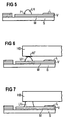
- Figure 4 also shows a deflectable laser beam LS3, with which in each case the solder layer L on a connection pad P1 on the lead area LB1 leading away from it and on that one leading solder supply structure LS melted at the same time becomes.
- an Nd: YAG laser with a wavelength of 1.06 ⁇ m used its laser beam LS3 strong is out of focus.
- solder bump LH With the described laser remelting of the solder layer L the liquid solder flows from the narrow solder supply structure L. S and from the narrow conductor area LB1 to the connection pad P1 out, so that there is a solder bump LH by itself according to FIG arises.
- the volume of the solder bump LH can be determined using of Figures 8 and 9 measures to be explained further enlarged become.
- Figure 6 shows the arrangement of a bumpless semiconductor device HB on the wiring, for example from a Layer sequence of aluminum, nickel and gold existing pads AF immediately on the tops of the assigned Lothöcker LH lie on. Then all of the semiconductor devices HB assigned to the LHöcker LH for example Reflow soldering or melted simultaneously by laser soldering, this results in reliable solder connections with the Figure 7 shows the concave shape of the solder bump LH.
- FIG. 8 shows a connection pad, designated P2 here, which via a constricted ladder area LB2 with the further one Conductor path LZ is connected. Also lead to the connection pad P2 a total of three blind-ended solder supply structures LS out, which is a corresponding increase in the solder volume of the solder bump created on connection pad P2 cause.
Landscapes
- Engineering & Computer Science (AREA)
- Microelectronics & Electronic Packaging (AREA)
- Manufacturing & Machinery (AREA)
- Electric Connection Of Electric Components To Printed Circuits (AREA)
- Wire Bonding (AREA)
- Laser Beam Processing (AREA)
Abstract
Description
- Bildung eines Leitermusters auf einem elektrisch isolierenden Substrat, wobei Anschluß-Pads des Leitermusters jeweils mit den zugeordneten weiterführenden Leiterzügen verbunden sind,
- Aufbringen einer Lotschicht auf die Anschluß-Pads und die Leiterzüge,
- Umschmelzen der Lotschicht in einem Bad zur Bildung der Lothöcker auf den Anschluß-Pads.
Es zeigen:
- Figur 1
- bis Figur 6 verschiedene Verfahrensstadien bei der Herstellung einer Verdrahtung und der Bildung von Lothöckern auf den Anschluß-Pads dieser Verdrahtung,
- Figur 7
- die fertige Verdrahtung nach dem Auflöten eines Halbleiterbausteins,
- Figur 8
- eine Variante mit mehreren zu den Anschluß-Pads hin führenden Lotzufuhrstrukturen und
- Figur 9
- eine Variante für die Bildung von in der Breite reduzierten Leiterstrukturen durch in die Leiterzüge mittig eingebrachte Löcher.
Claims (15)
- Verfahren zur Herstellung von Verdrahtungen mit Lothöckern (LH) für die Flipchip-Montage oder die Oberflächenmontage, mit folgenden Schritten:Bildung eines Leitermusters auf einem elektrisch isolierenden Substrat (S), wobei Anschluß-Pads (P1; P2; P3) des Leitermusters jeweils über in der Breite gegenüber der Breite der Leiterzüge (LZ) reduzierte Leiterbereiche (LB1; LB2; LB3) mit den zugeordneten weiterführenden Leiterzügen (LZ) verbunden sind,Aufbringen einer Lotschicht (L) auf das Leitermuster, zumindest im Bereich der Anschluß-Pads (P1; P2, P3) und der in der Breite reduzierten Leiterbereiche (LB1; LB2; LB3),Umschmelzen der Lotschicht (L) zur Bildung der Lothöcker (LH) auf den Anschluß-Pads (P1; P2; P3).
- Verfahren nach Anspruch 1, dadurch gekennzeichnet, daß die in der Breite reduzierten Leiterbereiche (LB1; LB2) durch eine Einschnürung der Leiterzüge (LZ) gebildet werden.
- Verfahren nach Anspruch 1, dadurch gekennzeichnet, daß die in der Breite reduzierten Leiterbereiche (LB3) durch das Einbringen eines Loches (LO) in den mittleren Bereich der Leiterzüge (LZ) gebildet werden.
- Verfahren nach einem der vorhergehenden Ansprüche, dadurch gekennzeichnet, daß Anschluß-Pads (P1; P2; P3) mit Flächenabmessungen zwischen 100x100 µm2 und 250x250 µm2 gebildet werden und daß in der Breite reduzierte Leiterbereiche (LB 1; LB2; LB3) mit einer Breite zwischen 10 µm und 40 µm und einer Länge zwischen 100 µm und 500 µm gebildet werden.
- Verfahren nach einem der vorhergehenden Ansprüche, dadurch gekennzeichnet, daß bei der Bildung des Leitermusters zusätzliche Lotzufuhrstrukturen (LS) erzeugt werden, wobei von den einzelnen Anschluß-Pads (P1; P2; P3) jeweils mindestens eine, in der Breite gegenüber der Breite der Leiterzüge (LZ) reduzierte Lotzufuhrstruktur (LS) wegführt.
- Verfahren nach Anspruch 5, dadurch gekennzeichnet, daß Lotzufuhrstrukturen (LS) mit einer Breite zwischen 10 µm und 40 µm und einer Länge zwischen 100 µm und 500 µm gebildet werden.
- Verfahren nach einem der vorhergehenden Ansprüche, dadurch gekennzeichnet, daß auf das Leitermuster eine aus einer Zinn-Blei-Legierung bestehende Lotschicht (L) aufgebracht wird.
- Verfahren nach einem der vorhergehenden Ansprüche, dadurch gekennzeichnet, daß die Lotschicht (L) durch galvanische Metallabscheidung auf das Leitermuster aufgebracht wird.
- Verfahren nach Anspruch 8, dadurch gekennzeichnet, daß die kathodische Kontaktierung des Leitermusters bei der galvanischen Metallabscheidung über eine mit sämtlichen Anschluß-Pads (P1; P2; P3) verbundene Sammelleitung (SL) vorgenommen wird und daß die Sammelleitung (SL) nach der Metallabscheidung abgetrennt wird.
- Verfahren nach einem der vorhergehenden Ansprüche, dadurch gekennzeichnet, daß die Lotschicht (L) mit Hilfe eines Laserstrahls (LS3) umgeschmolzen wird.
- Verfahren nach Anspruch 10, dadurch gekennzeichnet, daß die Lotschichten (L) jeweils selektiv im Bereich der Anschluß-Pads (P1; P2; P3) und der davon wegführenden, in der Breite reduzierten Leiterbereiche (LB1; LB2; LB3) umgeschmolzen werden.
- Verfahren nach den Ansprüchen 5 und 11, dadurch gekennzeichnet, daß die Lotschichten (L) jeweils selektiv im Bereich der Anschluß-Pads (P1; P2; P3), der davon wegführenden, in der Breite reduzierten Leiterbereiche (LB1; LB2; LB3) und der davon wegführenden Lotzufuhrstrukturen (LS) umgeschmolzen werden.
- Verfahren nach einem der Ansprüche 10 bis 12, dadurch gekennzeichnet, daß die Lotschichten (L) mit Hilfe eines stark außer Fokus gestellten Laserstrahls (LS3) umgeschmolzen werden.
- Verfahren nach einem der Ansprüche 10 bis 13, dadurch gekennzeichnet, daß die Lotschichten (L) mit dem Laserstrahl (LS3) eines Nd:YAG-Lasers mit einer Wellenlänge von 1,06 µm umgeschmolzen werden.
- Verfahren nach einem der Ansprüche 10 bis 14, dadurch gekennzeichnet, daß die Lotschichten (L) mit Hilfe eines ablenkbaren Laserstrahls (LS3) umgeschmolzen werden.
Applications Claiming Priority (3)
| Application Number | Priority Date | Filing Date | Title |
|---|---|---|---|
| DE19824633 | 1998-06-02 | ||
| DE19824633 | 1998-06-02 | ||
| PCT/EP1999/003802 WO1999063795A1 (de) | 1998-06-02 | 1999-06-01 | Verfahren zur herstellung von verdrahtungen mit lothöckern |
Publications (2)
| Publication Number | Publication Date |
|---|---|
| EP1082884A1 EP1082884A1 (de) | 2001-03-14 |
| EP1082884B1 true EP1082884B1 (de) | 2002-01-16 |
Family
ID=7869674
Family Applications (1)
| Application Number | Title | Priority Date | Filing Date |
|---|---|---|---|
| EP99927832A Expired - Lifetime EP1082884B1 (de) | 1998-06-02 | 1999-06-01 | Verfahren zur herstellung von verdrahtungen mit lothöckern |
Country Status (6)
| Country | Link |
|---|---|
| EP (1) | EP1082884B1 (de) |
| JP (1) | JP2002517908A (de) |
| KR (1) | KR20010071364A (de) |
| CN (1) | CN1304635A (de) |
| DE (1) | DE59900644D1 (de) |
| WO (1) | WO1999063795A1 (de) |
Family Cites Families (6)
| Publication number | Priority date | Publication date | Assignee | Title |
|---|---|---|---|---|
| US3778532A (en) * | 1972-07-03 | 1973-12-11 | Illinois Tool Works | Electrical circuit component having solder preform connection means |
| GB2143759B (en) * | 1983-01-24 | 1986-12-10 | Ford Motor Co | Method of laser soldering |
| US4926022A (en) * | 1989-06-20 | 1990-05-15 | Digital Equipment Corporation | Laser reflow soldering process and bonded assembly formed thereby |
| KR0125924B1 (ko) * | 1991-08-05 | 1997-12-26 | 안토니제이 살리 2세 | 납땜 범프를 회로 트레이스상에 형성하는 납땜 플레이트 역류 방법 |
| US5282565A (en) * | 1992-12-29 | 1994-02-01 | Motorola, Inc. | Solder bump interconnection formed using spaced solder deposit and consumable path |
| CN1179412C (zh) * | 1995-04-05 | 2004-12-08 | 统一国际有限公司 | 具有伸长部分和展宽部分的焊料结构及其形成方法 |
-
1999
- 1999-06-01 DE DE59900644T patent/DE59900644D1/de not_active Expired - Fee Related
- 1999-06-01 KR KR1020007013578A patent/KR20010071364A/ko not_active Withdrawn
- 1999-06-01 WO PCT/EP1999/003802 patent/WO1999063795A1/de not_active Ceased
- 1999-06-01 CN CN99806997A patent/CN1304635A/zh active Pending
- 1999-06-01 EP EP99927832A patent/EP1082884B1/de not_active Expired - Lifetime
- 1999-06-01 JP JP2000552882A patent/JP2002517908A/ja active Pending
Also Published As
| Publication number | Publication date |
|---|---|
| CN1304635A (zh) | 2001-07-18 |
| WO1999063795A1 (de) | 1999-12-09 |
| EP1082884A1 (de) | 2001-03-14 |
| JP2002517908A (ja) | 2002-06-18 |
| DE59900644D1 (de) | 2002-02-21 |
| KR20010071364A (ko) | 2001-07-28 |
Similar Documents
| Publication | Publication Date | Title |
|---|---|---|
| DE69434160T2 (de) | Mit Lötkugeln Verbindensverfahren damit versehen | |
| DE69132685T2 (de) | Halbleiteranordnung bestehend aus einem TAB-Band und deren Herstellungsverfahren | |
| DE10301512A1 (de) | Verkleinertes Chippaket und Verfahren zu seiner Herstellung | |
| DE19524739A1 (de) | Kernmetall-Lothöcker für die Flip-Chip-Technik | |
| DE10246892A1 (de) | LED-Matrix mit hoher Strahlungsleistung | |
| DE10148042A1 (de) | Elektronisches Bauteil mit einem Kunststoffgehäuse und Komponenten eines höhenstrukturierten metallischen Systemträgers und Verfahren zu deren Herstellung | |
| EP1450404A2 (de) | Anordnung in Druckkontaktierung mit einem Leistungshalbleitermodul | |
| DE69104683T2 (de) | System für das Zusammenschalten elektrischer Komponenten mit verschiedenen Verbindungserfordernissen zum Montieren der Komponenten auf Leiterplatten. | |
| DE69620273T2 (de) | Verfahren zur Herstellung von Abstandshaltern auf einer elektrischen Leiterplatte | |
| EP1106040B1 (de) | Verfahren zur herstellung von verdrahtungen mit elektrisch leitenden querverbindungen zwischen ober- und unterseite eines substrats sowie verdrahtung mit derartigen querverbindungen | |
| DE4446471C2 (de) | Verfahren zur Montage eines Chips auf einem flexiblen Schaltungsträger | |
| DE4301728C2 (de) | Leiterplatte mit lötbarer dünner Metallschicht zum Auflöten von elektronischen Bauelementen | |
| DE69015879T2 (de) | Verfahren zur Herstellung einer oberflächenmontierbaren Leiterplatte. | |
| DE102014118941B4 (de) | Bump-auf-Leitung (BAL)–Aufbau und Verfahren zur Ausbildung des BAL-Aufbaus | |
| DE102005004360A1 (de) | Effizientes Verfahren zum Herstellen und Zusammenfügen eines mikroelektronischen Chips mit Lothöckern | |
| DE19830158C2 (de) | Zwischenträgersubstrat mit hoher Verdrahtungsdichte für elektronische Bauelemente | |
| DE3343367A1 (de) | Halbleiterbauelement mit hoeckerartigen, metallischen anschlusskontakten und mehrlagenverdrahtung | |
| DE10017746A1 (de) | Elektronisches Bauteil mit mikroskopisch kleinen Kontaktflächen und Verfahren zu seiner Herstellung | |
| DE102016103552A1 (de) | Modul für eine Leuchte | |
| WO2020053160A1 (de) | Verfahren zur herstellung einer leiterplattenanordnung und leiterplattenanordnung | |
| DE10029269B4 (de) | Verfahren zur Herstellung eines elektronischen Bauteiles aus gehäusebildenden Substraten | |
| DE2443245A1 (de) | Verfahren zum herstellen einer multichip-verdrahtung | |
| WO1999063795A1 (de) | Verfahren zur herstellung von verdrahtungen mit lothöckern | |
| DE19743289A1 (de) | Mehrebenen-Zwischenträgersubstrat mit hoher Verdrahtungsdichte, insbesondere für Multichipmodule, und Verfahren zu seiner Herstellung | |
| DE10313047B3 (de) | Verfahren zur Herstellung von Chipstapeln |
Legal Events
| Date | Code | Title | Description |
|---|---|---|---|
| PUAI | Public reference made under article 153(3) epc to a published international application that has entered the european phase |
Free format text: ORIGINAL CODE: 0009012 |
|
| 17P | Request for examination filed |
Effective date: 20001114 |
|
| AK | Designated contracting states |
Kind code of ref document: A1 Designated state(s): BE CH DE FR GB IT LI NL |
|
| GRAG | Despatch of communication of intention to grant |
Free format text: ORIGINAL CODE: EPIDOS AGRA |
|
| GRAG | Despatch of communication of intention to grant |
Free format text: ORIGINAL CODE: EPIDOS AGRA |
|
| GRAH | Despatch of communication of intention to grant a patent |
Free format text: ORIGINAL CODE: EPIDOS IGRA |
|
| 17Q | First examination report despatched |
Effective date: 20010625 |
|
| GRAH | Despatch of communication of intention to grant a patent |
Free format text: ORIGINAL CODE: EPIDOS IGRA |
|
| GRAA | (expected) grant |
Free format text: ORIGINAL CODE: 0009210 |
|
| REG | Reference to a national code |
Ref country code: GB Ref legal event code: IF02 |
|
| AK | Designated contracting states |
Kind code of ref document: B1 Designated state(s): BE CH DE FR GB IT LI NL |
|
| REG | Reference to a national code |
Ref country code: CH Ref legal event code: EP |
|
| REF | Corresponds to: |
Ref document number: 59900644 Country of ref document: DE Date of ref document: 20020221 |
|
| REG | Reference to a national code |
Ref country code: CH Ref legal event code: NV Representative=s name: SIEMENS SCHWEIZ AG |
|
| GBT | Gb: translation of ep patent filed (gb section 77(6)(a)/1977) |
Effective date: 20020407 |
|
| ET | Fr: translation filed | ||
| PGFP | Annual fee paid to national office [announced via postgrant information from national office to epo] |
Ref country code: FR Payment date: 20020625 Year of fee payment: 4 Ref country code: BE Payment date: 20020625 Year of fee payment: 4 |
|
| PGFP | Annual fee paid to national office [announced via postgrant information from national office to epo] |
Ref country code: DE Payment date: 20020819 Year of fee payment: 4 |
|
| PLBE | No opposition filed within time limit |
Free format text: ORIGINAL CODE: 0009261 |
|
| STAA | Information on the status of an ep patent application or granted ep patent |
Free format text: STATUS: NO OPPOSITION FILED WITHIN TIME LIMIT |
|
| 26N | No opposition filed | ||
| PG25 | Lapsed in a contracting state [announced via postgrant information from national office to epo] |
Ref country code: GB Free format text: LAPSE BECAUSE OF NON-PAYMENT OF DUE FEES Effective date: 20030601 |
|
| PG25 | Lapsed in a contracting state [announced via postgrant information from national office to epo] |
Ref country code: LI Free format text: LAPSE BECAUSE OF NON-PAYMENT OF DUE FEES Effective date: 20030630 Ref country code: CH Free format text: LAPSE BECAUSE OF NON-PAYMENT OF DUE FEES Effective date: 20030630 Ref country code: BE Free format text: LAPSE BECAUSE OF NON-PAYMENT OF DUE FEES Effective date: 20030630 |
|
| BERE | Be: lapsed |
Owner name: S.A. *SIEMENS Effective date: 20030630 |
|
| PG25 | Lapsed in a contracting state [announced via postgrant information from national office to epo] |
Ref country code: NL Free format text: LAPSE BECAUSE OF NON-PAYMENT OF DUE FEES Effective date: 20040101 Ref country code: DE Free format text: LAPSE BECAUSE OF NON-PAYMENT OF DUE FEES Effective date: 20040101 |
|
| GBPC | Gb: european patent ceased through non-payment of renewal fee |
Effective date: 20030601 |
|
| REG | Reference to a national code |
Ref country code: CH Ref legal event code: PL |
|
| PG25 | Lapsed in a contracting state [announced via postgrant information from national office to epo] |
Ref country code: FR Free format text: LAPSE BECAUSE OF NON-PAYMENT OF DUE FEES Effective date: 20040227 |
|
| NLV4 | Nl: lapsed or anulled due to non-payment of the annual fee |
Effective date: 20040101 |
|
| REG | Reference to a national code |
Ref country code: FR Ref legal event code: ST |
|
| PG25 | Lapsed in a contracting state [announced via postgrant information from national office to epo] |
Ref country code: IT Free format text: LAPSE BECAUSE OF NON-PAYMENT OF DUE FEES Effective date: 20050601 |