EP1070352B1 - Halbleiter-speichervorrichtung und verfahren zu deren herstellung - Google Patents
Halbleiter-speichervorrichtung und verfahren zu deren herstellung Download PDFInfo
- Publication number
- EP1070352B1 EP1070352B1 EP99924679A EP99924679A EP1070352B1 EP 1070352 B1 EP1070352 B1 EP 1070352B1 EP 99924679 A EP99924679 A EP 99924679A EP 99924679 A EP99924679 A EP 99924679A EP 1070352 B1 EP1070352 B1 EP 1070352B1
- Authority
- EP
- European Patent Office
- Prior art keywords
- semiconductor memory
- contact
- region
- substrate
- semiconductor substrate
- Prior art date
- Legal status (The legal status is an assumption and is not a legal conclusion. Google has not performed a legal analysis and makes no representation as to the accuracy of the status listed.)
- Expired - Lifetime
Links
- 239000004065 semiconductor Substances 0.000 title claims description 52
- 238000004519 manufacturing process Methods 0.000 title description 12
- 239000000758 substrate Substances 0.000 claims description 28
- 238000002513 implantation Methods 0.000 claims description 23
- 238000000034 method Methods 0.000 claims description 10
- 239000002019 doping agent Substances 0.000 claims description 6
- 238000011156 evaluation Methods 0.000 claims description 4
- 239000011159 matrix material Substances 0.000 claims description 4
- 230000003247 decreasing effect Effects 0.000 claims 1
- 230000015654 memory Effects 0.000 description 15
- XUIMIQQOPSSXEZ-UHFFFAOYSA-N Silicon Chemical compound [Si] XUIMIQQOPSSXEZ-UHFFFAOYSA-N 0.000 description 4
- 238000009792 diffusion process Methods 0.000 description 4
- 229910052710 silicon Inorganic materials 0.000 description 4
- 239000010703 silicon Substances 0.000 description 4
- 229910000838 Al alloy Inorganic materials 0.000 description 3
- 238000013459 approach Methods 0.000 description 3
- 238000010586 diagram Methods 0.000 description 3
- 239000012535 impurity Substances 0.000 description 2
- 229910021420 polycrystalline silicon Inorganic materials 0.000 description 2
- 229920005591 polysilicon Polymers 0.000 description 2
- 238000003860 storage Methods 0.000 description 2
- WFKWXMTUELFFGS-UHFFFAOYSA-N tungsten Chemical compound [W] WFKWXMTUELFFGS-UHFFFAOYSA-N 0.000 description 2
- 239000010937 tungsten Substances 0.000 description 2
- 229910052721 tungsten Inorganic materials 0.000 description 2
- 230000015572 biosynthetic process Effects 0.000 description 1
- 239000004020 conductor Substances 0.000 description 1
- 238000005530 etching Methods 0.000 description 1
- 230000002349 favourable effect Effects 0.000 description 1
- 239000007943 implant Substances 0.000 description 1
- 238000009830 intercalation Methods 0.000 description 1
- 238000005468 ion implantation Methods 0.000 description 1
- 238000002955 isolation Methods 0.000 description 1
- 238000002360 preparation method Methods 0.000 description 1
- 229910021341 titanium silicide Inorganic materials 0.000 description 1
Images
Classifications
-
- H—ELECTRICITY
- H10—SEMICONDUCTOR DEVICES; ELECTRIC SOLID-STATE DEVICES NOT OTHERWISE PROVIDED FOR
- H10B—ELECTRONIC MEMORY DEVICES
- H10B20/00—Read-only memory [ROM] devices
-
- H—ELECTRICITY
- H10—SEMICONDUCTOR DEVICES; ELECTRIC SOLID-STATE DEVICES NOT OTHERWISE PROVIDED FOR
- H10D—INORGANIC ELECTRIC SEMICONDUCTOR DEVICES
- H10D84/00—Integrated devices formed in or on semiconductor substrates that comprise only semiconducting layers, e.g. on Si wafers or on GaAs-on-Si wafers
- H10D84/01—Manufacture or treatment
- H10D84/02—Manufacture or treatment characterised by using material-based technologies
- H10D84/03—Manufacture or treatment characterised by using material-based technologies using Group IV technology, e.g. silicon technology or silicon-carbide [SiC] technology
- H10D84/038—Manufacture or treatment characterised by using material-based technologies using Group IV technology, e.g. silicon technology or silicon-carbide [SiC] technology using silicon technology, e.g. SiGe
Definitions
- the present invention relates to a semiconductor memory device and a method of manufacturing the same.
- Revealed in the DE 40 08 833 A is a method of fabricating a mask ROM having an array of memory cells in which pn junctions formed by incorporating P-type impurities by ion implantation into the surface of N-type electroconductive layers, again by intercalating N-type impurities Polysilicon layers have been obtained, are formed as memory cells in a matrix configuration.
- the JP 59 067666 A discloses a read-only memory in which pn-junctions generated with contact holes as a mask are used as memory cells.
- the US-A-5,621,247 discloses a memory device having memory cells each consisting of a tungsten electrode and a silicon-containing aluminum alloy electrode.
- memory cells each consisting of a tungsten electrode and a silicon-containing aluminum alloy electrode.
- silicon in the aluminum alloy electrode moves counter to the current flow direction and is deposited in the aluminum alloy electrode in the vicinity of the interface with the tungsten electrode, resulting in an increased resistance value.
- Data can be read by measuring the magnitude of the resistance value with an extremely small current and judging whether it is in a high or low state.
- CMOS memory devices of this type use horizontal or vertical MOSFETs as semiconductor memory cells.
- a common method of programming such ROM memories is to modify the threshold voltages of the MOSFETs used in the ROM cell array according to the desired ROM contents by appropriately masked vertical channel implantations.
- MOSFETs are created, a first type having a first threshold voltage (e.g., without channel implantation) and a second type having a second threshold voltage (e.g., channel implantation).
- One type is assigned the logical "1" and the other type the logical "0".
- each transistor can store a single bit.
- One objective in memory development is to increase the storage density, i. the number of bits which can be stored per unit area or volume unit.
- One approach in this direction is the continuous reduction of the structures involved, for example by ROM storage with folded trench structures.
- Another approach is to modify the semiconductor memory elements such that they can each store more than one bit. This can be achieved, for example, by performing more than one type of channel implantation so that one bit per memory cell can be stored for each channel implantation.
- four different threshold voltages ie 2 bits per memory cell
- four different threshold voltages can be generated with four different channel implantations.
- the different threshold voltages can be distinguished.
- the object of the present invention is to provide a simplified semiconductor memory device whose semiconductor memory elements can store more than one bit and a method for the production thereof.
- this object is achieved by the semiconductor memory device specified in claim 1 and the manufacturing method specified in claim 2.
- the respective bit-setting region is designed such that it defines the contact resistance between the substrate region and the contact plug region in accordance with the bit to be stored in the respective semiconductor memory element.
- the via implant mask is used for programming with the contact holes provided with a different contact resistance.
- the various resistors can then be evaluated during readout by a suitable evaluation circuit.
- the evaluation circuit may have a resistance measuring device, but may also work capacitively or inductively.
- the semiconductor memory device according to the invention and the method according to the invention for the production thereof have, among other things, the following advantages over the known approaches. It can be realized with only two implantations a trivalent logic per memory cell. This means that, for example, three bits can be stored in two cells. This saves a mask level in comparison to the method described above for MOSFETs.
- the programming takes place late in the process after the contact hole etching, which allows a favorable turn-around time. For security-relevant applications, such as in the chip card area is a subsequent readout by re-preparation is difficult.
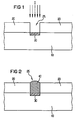
- FIG. 12 is a schematic diagram of a manufacturing step of a semiconductor memory element of the semiconductor memory device according to a first embodiment of the present invention.
- Fig. 1 10 is a substrate, 20 is an insulating layer, 25 is a contact hole, 30 is a bit attaching region, 40 is a contact plug region, and I is an implantation.
- the method for manufacturing the semiconductor memory device according to the first embodiment of the present invention is as follows.
- the substrate 10 of the first conductivity type (e.g., n-type silicon) is provided.
- the term substrate should be understood in the general sense, so does not have to be the physical support, but may also have an epilayer located thereon, a diffusion area provided therein or the like. be.
- the isolation layer 20 is provided on the substrate 10 in which a matrix of contact holes 25 is to be formed to the substrate 10 corresponding to respective semiconductor memory elements.
- the surface area of the substrate 10 located beneath the contact holes 25 is provided with a respective contact resistance corresponding to that in the respective semiconductor memory element to be stored bit provided as Bitfestlegungs Society 30 of the relevant semiconductor memory element.
- All contact holes 25 are photolithographically defined and etched free. Then, the first implantation I is performed in this first group of contact holes 25 with a dopant of the first conductivity type n.
- a second implantation is performed with a dopant of the second conductivity type p.
- the third group of contact holes 25 remains covered during the two implantations, so receives no implantation.
- contact implantation such as underlying substrate (eg, such as diffusion implantation), no implantation and contact implantation opposite to the underlying substrate, wherein Fig. 1 only the first case shows.
- FIG. 12 is a schematic diagram of another manufacturing step of the semiconductor memory element of the semiconductor memory device according to the first embodiment of the present invention.
- FIG. 12 is a schematic diagram of another manufacturing step of the semiconductor memory element of the semiconductor memory device according to the first embodiment of the present invention.
- Fig. 2 in addition to the already introduced reference numeral 40 denotes a contact plug.
- contact plugs 40 are formed in the contact holes 25, which are in electrical contact with the bit setting area 30 are provided.
- the substrate portion 10 has a strip-shaped conductor strip structure, e.g. Polysilicon or diffusion strips, these strips each form the second terminal of the memory cells on the substrate top side, which forms a connection for an evaluation circuit with a resistance measuring device next to the respective contact plug 40.
- a strip-shaped conductor strip structure e.g. Polysilicon or diffusion strips
Landscapes
- Semiconductor Memories (AREA)
- Semiconductor Integrated Circuits (AREA)
Applications Claiming Priority (3)
| Application Number | Priority Date | Filing Date | Title |
|---|---|---|---|
| DE19815874 | 1998-04-08 | ||
| DE19815874A DE19815874C2 (de) | 1998-04-08 | 1998-04-08 | ROM-Halbleiter-Speichervorrichtung mit Implantationsbereichen zur Einstellung eines Kontaktwiderstandes und Verfahren zu deren Herstellung |
| PCT/DE1999/000901 WO1999053546A1 (de) | 1998-04-08 | 1999-03-25 | Halbleiter-speichervorrichtung und verfahren zu deren herstellung |
Publications (2)
| Publication Number | Publication Date |
|---|---|
| EP1070352A1 EP1070352A1 (de) | 2001-01-24 |
| EP1070352B1 true EP1070352B1 (de) | 2008-08-13 |
Family
ID=7864069
Family Applications (1)
| Application Number | Title | Priority Date | Filing Date |
|---|---|---|---|
| EP99924679A Expired - Lifetime EP1070352B1 (de) | 1998-04-08 | 1999-03-25 | Halbleiter-speichervorrichtung und verfahren zu deren herstellung |
Country Status (7)
| Country | Link |
|---|---|
| US (1) | US7230877B1 (enExample) |
| EP (1) | EP1070352B1 (enExample) |
| JP (1) | JP2002511655A (enExample) |
| KR (1) | KR100408944B1 (enExample) |
| DE (2) | DE19815874C2 (enExample) |
| TW (1) | TW404026B (enExample) |
| WO (1) | WO1999053546A1 (enExample) |
Families Citing this family (3)
| Publication number | Priority date | Publication date | Assignee | Title |
|---|---|---|---|---|
| KR100666174B1 (ko) | 2005-04-27 | 2007-01-09 | 삼성전자주식회사 | 3-레벨 불휘발성 반도체 메모리 장치 및 이에 대한구동방법 |
| KR101391881B1 (ko) | 2007-10-23 | 2014-05-07 | 삼성전자주식회사 | 멀티-비트 플래시 메모리 장치 및 그것의 프로그램 및 읽기방법 |
| CN102456693A (zh) * | 2010-10-27 | 2012-05-16 | 上海华虹Nec电子有限公司 | 掩膜型rom器件的单元结构 |
Family Cites Families (10)
| Publication number | Priority date | Publication date | Assignee | Title |
|---|---|---|---|---|
| JPS5967666A (ja) * | 1982-10-09 | 1984-04-17 | Mitsubishi Electric Corp | Rom |
| JP2508247B2 (ja) * | 1989-03-20 | 1996-06-19 | 三菱電機株式会社 | マスクromの製造方法 |
| US5526306A (en) * | 1994-02-10 | 1996-06-11 | Mega Chips Corporation | Semiconductor memory device and method of fabricating the same |
| JPH0837164A (ja) * | 1994-07-21 | 1996-02-06 | Nec Corp | 半導体装置の製造方法 |
| TW287313B (enExample) * | 1995-02-20 | 1996-10-01 | Matsushita Electric Industrial Co Ltd | |
| JP3586332B2 (ja) * | 1995-02-28 | 2004-11-10 | 新日本製鐵株式会社 | 不揮発性半導体記憶装置及びその製造方法 |
| US5563098A (en) * | 1995-04-10 | 1996-10-08 | Taiwan Semiconductor Manufacturing Company | Buried contact oxide etch with poly mask procedure |
| JP3185862B2 (ja) * | 1997-09-10 | 2001-07-11 | 日本電気株式会社 | マスク型半導体装置の製造方法 |
| US6030871A (en) * | 1998-05-05 | 2000-02-29 | Saifun Semiconductors Ltd. | Process for producing two bit ROM cell utilizing angled implant |
| US6200861B1 (en) * | 1999-03-26 | 2001-03-13 | Taiwan Semiconductor Manufacturing Co., Ltd. | Method of fabricating high density multiple states mask ROM cells |
-
1998
- 1998-04-08 DE DE19815874A patent/DE19815874C2/de not_active Expired - Fee Related
-
1999
- 1999-03-25 EP EP99924679A patent/EP1070352B1/de not_active Expired - Lifetime
- 1999-03-25 WO PCT/DE1999/000901 patent/WO1999053546A1/de not_active Ceased
- 1999-03-25 DE DE59914831T patent/DE59914831D1/de not_active Expired - Lifetime
- 1999-03-25 JP JP2000544011A patent/JP2002511655A/ja not_active Ceased
- 1999-03-25 KR KR10-2000-7011234A patent/KR100408944B1/ko not_active Expired - Fee Related
- 1999-04-08 TW TW088105428A patent/TW404026B/zh not_active IP Right Cessation
-
2000
- 2000-10-10 US US09/685,361 patent/US7230877B1/en not_active Expired - Fee Related
Also Published As
| Publication number | Publication date |
|---|---|
| DE59914831D1 (de) | 2008-09-25 |
| KR100408944B1 (ko) | 2003-12-11 |
| DE19815874A1 (de) | 1999-10-14 |
| DE19815874C2 (de) | 2002-06-13 |
| US7230877B1 (en) | 2007-06-12 |
| WO1999053546A1 (de) | 1999-10-21 |
| TW404026B (en) | 2000-09-01 |
| EP1070352A1 (de) | 2001-01-24 |
| JP2002511655A (ja) | 2002-04-16 |
| KR20010042569A (ko) | 2001-05-25 |
Similar Documents
| Publication | Publication Date | Title |
|---|---|---|
| DE4241457B4 (de) | P-leitendes floatendes Gate aus Poly-Silizium zur Verwendung bei einem Halbleiterbautransistorelement und daraus hergestelltes Flash-E2PROM | |
| DE10306281B4 (de) | Anordnung und Verfahren zur Herstellung von vertikalen Transistorzellen und transistorgesteuerten Speicherzellen | |
| DE4114344C2 (de) | Herstellungsverfahren und Aufbau einer nicht-flüchtigen Halbleiterspeichereinrichtung mit einer Speicherzellenanordnung und einem peripheren Schaltkreis | |
| DE69132387T2 (de) | Verfahren zum Herstellen einer Feldeffektanordnung mit Kanal aus polykristallinem Silizium | |
| DE3204039A1 (de) | Halbleiterspeicheranordnung und verfahren zu ihrer herstellung | |
| DE69013094T2 (de) | Nichtflüchtige Halbleiterspeicheranordnung und Verfahren zu ihrer Herstellung. | |
| DE3910033A1 (de) | Halbleiterspeicher und verfahren zu dessen herstellung | |
| DE69226223T2 (de) | Kontaktausrichtung für Festwertspeicher | |
| DE19501557A1 (de) | Halbleitervorrichtung und Verfahren zu deren Herstellung | |
| DE4209364A1 (de) | Cmos-sram und verfahren zu dessen herstellung | |
| DE69330302T2 (de) | Halbleiterspeicheranordnung und Verfahren zu ihrer Herstellung | |
| EP1145319B1 (de) | Integrierte schaltungsanordnung und verfahren zu deren herstellung | |
| DE2937952C2 (de) | Nichtflüchtige Speicheranordnung | |
| WO1999044238A1 (de) | Elektrisch programmierbare speicherzellenanordnung und verfahren zu deren herstellung | |
| EP0931340B1 (de) | Halbleiter-festwertspeicher und verfahren zu seiner herstellung | |
| DE69030946T2 (de) | Nichtflüchtige Halbleiterspeicheranordnung und Verfahren zu ihrer Herstellung | |
| EP1070352B1 (de) | Halbleiter-speichervorrichtung und verfahren zu deren herstellung | |
| DE19525576B4 (de) | Verfahren zur Herstellung eines Dünnfilmtransistors | |
| DE3230067A1 (de) | Permanentspeichervorrichtung | |
| DE69231030T2 (de) | Entwurf statischer Speicherzellen | |
| DE10314595A1 (de) | Verfahren zur Herstellung von Transistoren unterschiedlichen Leitungstyps und unterschiedlicher Packungsdichte in einem Halbleitersubstrat | |
| DE10256200A1 (de) | Flash-Speicherzelle und Verfahren zur Herstellung dieser, sowie ein Programmier-/Lösch-/Lese-Verfahren in der Flash-Speicherzelle | |
| DE2543138B2 (de) | Decoder, bestehend aus einem monolithischen, maskenprogrammierbaren Halbleiter-Festwertspeicher | |
| DE10250872B4 (de) | Verfahren zur Herstellung einer Halbleiterstruktur mit mehreren Gate-Stapeln | |
| EP1623459B1 (de) | Bitleitungsstruktur sowie verfahren zu deren herstellung |
Legal Events
| Date | Code | Title | Description |
|---|---|---|---|
| PUAI | Public reference made under article 153(3) epc to a published international application that has entered the european phase |
Free format text: ORIGINAL CODE: 0009012 |
|
| 17P | Request for examination filed |
Effective date: 20001010 |
|
| AK | Designated contracting states |
Kind code of ref document: A1 Designated state(s): DE FR GB IT |
|
| 17Q | First examination report despatched |
Effective date: 20060920 |
|
| GRAP | Despatch of communication of intention to grant a patent |
Free format text: ORIGINAL CODE: EPIDOSNIGR1 |
|
| GRAS | Grant fee paid |
Free format text: ORIGINAL CODE: EPIDOSNIGR3 |
|
| GRAA | (expected) grant |
Free format text: ORIGINAL CODE: 0009210 |
|
| AK | Designated contracting states |
Kind code of ref document: B1 Designated state(s): DE FR GB IT |
|
| REG | Reference to a national code |
Ref country code: GB Ref legal event code: FG4D Free format text: NOT ENGLISH |
|
| REF | Corresponds to: |
Ref document number: 59914831 Country of ref document: DE Date of ref document: 20080925 Kind code of ref document: P |
|
| PLBE | No opposition filed within time limit |
Free format text: ORIGINAL CODE: 0009261 |
|
| STAA | Information on the status of an ep patent application or granted ep patent |
Free format text: STATUS: NO OPPOSITION FILED WITHIN TIME LIMIT |
|
| 26N | No opposition filed |
Effective date: 20090514 |
|
| PG25 | Lapsed in a contracting state [announced via postgrant information from national office to epo] |
Ref country code: IT Free format text: LAPSE BECAUSE OF FAILURE TO SUBMIT A TRANSLATION OF THE DESCRIPTION OR TO PAY THE FEE WITHIN THE PRESCRIBED TIME-LIMIT Effective date: 20080813 |
|
| GBPC | Gb: european patent ceased through non-payment of renewal fee |
Effective date: 20090325 |
|
| PG25 | Lapsed in a contracting state [announced via postgrant information from national office to epo] |
Ref country code: GB Free format text: LAPSE BECAUSE OF NON-PAYMENT OF DUE FEES Effective date: 20090325 |
|
| PGFP | Annual fee paid to national office [announced via postgrant information from national office to epo] |
Ref country code: DE Payment date: 20110517 Year of fee payment: 13 |
|
| PGFP | Annual fee paid to national office [announced via postgrant information from national office to epo] |
Ref country code: FR Payment date: 20120403 Year of fee payment: 14 |
|
| REG | Reference to a national code |
Ref country code: DE Ref legal event code: R119 Ref document number: 59914831 Country of ref document: DE Effective date: 20121002 |
|
| REG | Reference to a national code |
Ref country code: FR Ref legal event code: ST Effective date: 20131129 |
|
| PG25 | Lapsed in a contracting state [announced via postgrant information from national office to epo] |
Ref country code: FR Free format text: LAPSE BECAUSE OF NON-PAYMENT OF DUE FEES Effective date: 20130402 |
|
| PG25 | Lapsed in a contracting state [announced via postgrant information from national office to epo] |
Ref country code: DE Free format text: LAPSE BECAUSE OF NON-PAYMENT OF DUE FEES Effective date: 20121002 |