EP1069482A2 - Rouleau conducteur, unité de traitement et appareil de formation d'images - Google Patents
Rouleau conducteur, unité de traitement et appareil de formation d'images Download PDFInfo
- Publication number
- EP1069482A2 EP1069482A2 EP00114847A EP00114847A EP1069482A2 EP 1069482 A2 EP1069482 A2 EP 1069482A2 EP 00114847 A EP00114847 A EP 00114847A EP 00114847 A EP00114847 A EP 00114847A EP 1069482 A2 EP1069482 A2 EP 1069482A2
- Authority
- EP
- European Patent Office
- Prior art keywords
- rubber
- conductive roller
- elastic layer
- electroconductive
- parts
- Prior art date
- Legal status (The legal status is an assumption and is not a legal conclusion. Google has not performed a legal analysis and makes no representation as to the accuracy of the status listed.)
- Granted
Links
Images
Classifications
-
- G—PHYSICS
- G03—PHOTOGRAPHY; CINEMATOGRAPHY; ANALOGOUS TECHNIQUES USING WAVES OTHER THAN OPTICAL WAVES; ELECTROGRAPHY; HOLOGRAPHY
- G03G—ELECTROGRAPHY; ELECTROPHOTOGRAPHY; MAGNETOGRAPHY
- G03G15/00—Apparatus for electrographic processes using a charge pattern
-
- G—PHYSICS
- G03—PHOTOGRAPHY; CINEMATOGRAPHY; ANALOGOUS TECHNIQUES USING WAVES OTHER THAN OPTICAL WAVES; ELECTROGRAPHY; HOLOGRAPHY
- G03G—ELECTROGRAPHY; ELECTROPHOTOGRAPHY; MAGNETOGRAPHY
- G03G15/00—Apparatus for electrographic processes using a charge pattern
- G03G15/02—Apparatus for electrographic processes using a charge pattern for laying down a uniform charge, e.g. for sensitising; Corona discharge devices
- G03G15/0208—Apparatus for electrographic processes using a charge pattern for laying down a uniform charge, e.g. for sensitising; Corona discharge devices by contact, friction or induction, e.g. liquid charging apparatus
- G03G15/0216—Apparatus for electrographic processes using a charge pattern for laying down a uniform charge, e.g. for sensitising; Corona discharge devices by contact, friction or induction, e.g. liquid charging apparatus by bringing a charging member into contact with the member to be charged, e.g. roller, brush chargers
- G03G15/0233—Structure, details of the charging member, e.g. chemical composition, surface properties
-
- G—PHYSICS
- G03—PHOTOGRAPHY; CINEMATOGRAPHY; ANALOGOUS TECHNIQUES USING WAVES OTHER THAN OPTICAL WAVES; ELECTROGRAPHY; HOLOGRAPHY
- G03G—ELECTROGRAPHY; ELECTROPHOTOGRAPHY; MAGNETOGRAPHY
- G03G2221/00—Processes not provided for by group G03G2215/00, e.g. cleaning or residual charge elimination
- G03G2221/16—Mechanical means for facilitating the maintenance of the apparatus, e.g. modular arrangements and complete machine concepts
- G03G2221/18—Cartridge systems
- G03G2221/183—Process cartridge
-
- Y—GENERAL TAGGING OF NEW TECHNOLOGICAL DEVELOPMENTS; GENERAL TAGGING OF CROSS-SECTIONAL TECHNOLOGIES SPANNING OVER SEVERAL SECTIONS OF THE IPC; TECHNICAL SUBJECTS COVERED BY FORMER USPC CROSS-REFERENCE ART COLLECTIONS [XRACs] AND DIGESTS
- Y10—TECHNICAL SUBJECTS COVERED BY FORMER USPC
- Y10T—TECHNICAL SUBJECTS COVERED BY FORMER US CLASSIFICATION
- Y10T428/00—Stock material or miscellaneous articles
- Y10T428/24—Structurally defined web or sheet [e.g., overall dimension, etc.]
- Y10T428/24942—Structurally defined web or sheet [e.g., overall dimension, etc.] including components having same physical characteristic in differing degree
-
- Y—GENERAL TAGGING OF NEW TECHNOLOGICAL DEVELOPMENTS; GENERAL TAGGING OF CROSS-SECTIONAL TECHNOLOGIES SPANNING OVER SEVERAL SECTIONS OF THE IPC; TECHNICAL SUBJECTS COVERED BY FORMER USPC CROSS-REFERENCE ART COLLECTIONS [XRACs] AND DIGESTS
- Y10—TECHNICAL SUBJECTS COVERED BY FORMER USPC
- Y10T—TECHNICAL SUBJECTS COVERED BY FORMER US CLASSIFICATION
- Y10T428/00—Stock material or miscellaneous articles
- Y10T428/28—Web or sheet containing structurally defined element or component and having an adhesive outermost layer
Definitions
- the present invention relates to an (electro-)conductive roller, and a process cartridge and an image forming apparatus including the conductive roller. More specifically, the present invention relates to a conductive roller used as a charging member for charging a surface of an electrophotographic photosensitive member as a member to be charged to a prescribed potential by voltage application, and a process cartridge and an image forming apparatus including such a conductive roller.
- a contact charging member for charging an electrophotographic photosensitive member in an image forming apparatus there has been conventionally used a charging roller comprising an electroconductive support (core metal) coated successively with an electroconductive elastic layer and a resistance layer.
- an AC+DC-charging scheme of applying a superposition of AC voltage and DC voltage to the core metal has been principally adopted.
- the AC voltage used for realizing charging uniformity has been set to have a peak-to-peak voltage Vpp which is at least two times a charging initiation voltage under DC voltage application.
- Vpp peak-to-peak voltage
- a DC charging scheme of applying only a DC voltage to a contact charging member has been commercialized.
- a conventional charging roller used as a contact charging member has more specifically a structure including an electroconductive support (core metal) coated with an electroconductive elastic layer for providing uniform abutment against an electrophotographic photosensitive member as a member to be charged and further with a resistance layer for resistivity adjustment, wear resistance and prevention of sticking onto the photosensitive member.
- a structure is also known including optionally an intermediate layer for resistivity adjustment or prevention of exudation of low-molecular weight component from the elastic layer.
- the electroconductive support a metal bar of iron, stainless steel, etc., has been used.
- the electroconductive elastic layer has been formed as a layer of elastomers or rubber, such as ethylene-propylene rubber (EPDM), butadiene rubber (BR), isoprene roller (IR), styrene-butadiene rubber (SBR), nitrile-butadiene rubber (NBR) or silicone rubber, containing electroconductive inorganic particles, such as electroconductive carbon black, dispersed therein for resistivity adjustment.
- EPDM ethylene-propylene rubber
- BR butadiene rubber
- IR isoprene roller
- SBR styrene-butadiene rubber
- NBR nitrile-butadiene rubber
- silicone rubber containing electroconductive inorganic particles, such as electroconductive carbon black, dispersed therein for resistivity adjustment.
- the resistance layer has been formed of a resin, such as polyamide resin or polyurethane resin, containing electroconductive inorganic particles of, e.g., carbon black, titanium oxide or tin oxide, dispersed therein for resistivity adjustment.
- a resin such as polyamide resin or polyurethane resin
- electroconductive inorganic particles e.g., carbon black, titanium oxide or tin oxide
- the charging performances inclusive of charging uniformity of the charging member, are liable to be affected by good or poor dispersion of the electroconductive particles in the electroconductive elastic layer in not a few cases.
- poor dispersion of electroconductive carbon black in the rubber has resulted in resistance irregularity of the charging member, leading to occurrence of density irregularity or black spots corresponding to rotation periods of the charging member is halftone images or solid white images.
- the influence of such dispersion irregularity has occurred more frequently in the case of the DC charging scheme applying only a DC voltage.
- ionic conductive agents such as alkaline metal salts of perchloric acid and long-chain alkylsulfonic acids, and tetraalkyl-quaternary ammonium salts.
- the use of such a known ionic conductive agent provides an improved dispersibility of the conductive agent, a larger fluctuation of resistivity is liable to be caused by a change of environmental condition.
- the charging member is liable to show a higher resistivity in a low humidity environment and a lower resistivity in a high humidity environment.
- the ionic conductive agent is liable to bleed out of the electroconductive elastic layer with time, thus changing the resistivity of the charging member.
- the ionic conductive agent having bled out of the electroconductive elastic layer migrates to the surface of the resistance layer, thereby causing cracks in the surface of the electroconductive photosensitive member contacting the charging member and sticking with the photosensitive member. Further, because of the ionic conductive agent having migrated to the surface of the resistance layer, the developer is liable to be attached to the charging member surface, thus causing a periodical density irregularity in the resultant images corresponding to the rotation period of the charging member.
- an object of the present invention is to provide a conductive roller as a photosensitive member capable of stably providing high-quality images for a long period.
- Another object of the present invention is to provide a process cartridge and an image forming apparatus including such a conductive roller.
- a conductive roller comprising:
- the present invention further provides:
- the (electro-)conductive roller according to the present invention may suitably be used as charging means, developing means, transfer means, cleaning means, etc., in electrophotographic image forming apparatus, such as copying machines and printers.
- the conductive roller according to the present invention comprises: an electroconductive support, an electroconductive elastic layer coating the support and a resistance layer coating the elastic layer; wherein
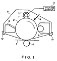
- Figure 1 schematically illustrates an embodiment of the image forming apparatus according to the present invention, which includes a process cartridge including a conductive roller according to the present invention.
- an electrophotographic photosensitive member in the form of a rotatable drum (hereinafter sometimes called a "photosensitive drum") 2 is rotated in a clockwise direction as indicated by an arrow at a peripheral speed (process speed).
- the photosensitive drum 2 may be formed of an electroconductive drum support of, e.g., aluminum or stainless steel, and a photosensitive layer coating an outer peripheral surface of the drum support.
- a conductive roller 1 according to the present invention as a contact charging member is disposed in parallel with the generatrix of the photosensitive rum 1 and pressed against the surface of the photosensitive drum 2 at a prescribed pressure and is rotated mating with the rotation of the photosensitive drum 2.
- the charging roller 1 may be driven in rotation by a separate drive mechanism.
- the charging roller 1 includes a core metal 1a, to which a prescribed voltage is applied from a voltage supply source. As a result, the outer peripheral surface of the rotating photosensitive drum 2 is charged to a prescribed potential of a prescribed polarity.
- the charging member 1 may preferably be supplied with a DC voltage corresponding to a desired surface potential Vd of the photosensitive drum 2 in superposition with an AC voltage having a peak-to-peak voltage which is at least 2 times a charge initiation voltage Vth.
- the conductive roller of the present invention has a very excellent uniform conductivity, it is particularly suitably used in the DC charging scheme wherein the charging performance is liable to be ununiform.
- the surface of the photosensitive drum 2 thus primarily charged to a prescribed surface potential is sequentially subjected to exposure to imagewise scanning laser beam 4 carrying objective image data supplied from a laser scanner (exposure means, not shown), toner development with developing means 5, and transfer of the resultant toner image by transfer means 6 onto a transfer(-receiving) material 7 (such as paper), and the transfer material 7 carrying the transferred toner image and separated from the photosensitive drum 2 surface is then supplied to fixing means (not shown) to output an image product (copy or print).
- the photosensitive drum 2 surface after the toner image transfer is cleaned by cleaning means 8 for removal of attached soiling materials such as transfer residual toner, and then subjected to a new image forming cycle.
- the present invention is also applicable to a so-called cleanerless system which is not provided with independent cleaning means, such as a cleaning blade, a cleaning roller and a waste toner vessel and in which transfer residual toner (developer) is recovered electrostatically by the developing means.
- a so-called cleanerless system which is not provided with independent cleaning means, such as a cleaning blade, a cleaning roller and a waste toner vessel and in which transfer residual toner (developer) is recovered electrostatically by the developing means.
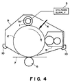
- An example of image forming apparatus according to such a cleanerless system is illustrated in Figure 4, wherein identical reference numerals are used for representing like members as in Figure 1.
- the photosensitive drum 2 and the charging member 1, and optionally further the developing means 5 (and cleaning means) can be integrally supported to form a process cartridge 9, which is detachably mountable to a main assembly of the image forming apparatus.
- a process cartridge 9 which is detachably mountable to a main assembly of the image forming apparatus.
- the inclusion of such a process cartridge is not essential in the image forming apparatus according to the present invention.
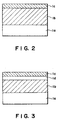
- Figures 2 and 3 respectively illustrate an example of layer structure for constituting a conductive roller according to the present invention.
- the conductive roller according to the present invention comprises an electroconductive support 1a, and at least an electroconductive elastic layer 1b and a resistance layer 1c disposed in this order on the electroconductive support 1a.
- an intermediate layer 1d can be inserted between the electroconductive elastic layer 1b and the resistance layer 1c for the purpose of resistivity adjustment or preventing bleeding-out of the plasticizer and the softening oil from the electroconductive elastic layer.
- the electroconductive support (core metal 1a, a cylindrical bar of a metal, such as iron, copper, nickel, stainless steel or brass, may be used as it is or after a surface-treatment, such as chemical nickel plating or chromium plating, for the purpose of rust prevention or wear resistance.
- a surface-treatment such as chemical nickel plating or chromium plating, for the purpose of rust prevention or wear resistance.
- the surface treatment should be performed with care for not imparsing the electroconductivity.
- the conductive elastic layer 1b of the conductive roller is formed of an elastomeric material for providing a uniform contact portion between the conductive roller and the electrophotographic photosensitive member.
- the elastomeric material first comprises a rubber.
- a rubber selected from the group consisting of acrylonitrile-butadiene rubber (NBR), epichlorohydrin homopolymer, ECO (epichlorohydrin-ethylene oxide copolymer), GECO (epichlorohydrin-ethylene oxide-ally glycidyl ether terpolymer), and GCO (epichlorohydrinalkyl glycidyl ether copolymer), and chloroprene rubber, all of which may be characterized as polar rubbers.
- NBR acrylonitrile-butadiene rubber
- ECO epichlorohydrin-ethylene oxide copolymer
- GECO epichlorohydrin-ethylene oxide-ally glycidyl ether terpolymer
- epichlorohydrin rubber is particularly prepared because it allows easy control of the resistivity of the resultant electroconductive elastic layer.
- NBR one having an acrylonitrile content of at least 25 wt. % (and preferably 45 wt. % or less) is preferred, since so-called low-nitrile NBR having an acrylonitrile content of 20 wt. % or below is liable to cause bleeding out of the above-mentioned additives because of relatively poor mutual solubility.
- non-polar rubber such as ethylene-propylene rubber or butadiene rubber is not preferred in the present invention because of bleeding-out to the surface of the additives.
- the above-mentioned polar rubber may be used in a blend with another type of rubber.
- the content of the polar rubber selected from acrylonitrile-butadiene rubber, epichlorohydrin rubber and chloroprene rubber, should preferably occupy at least 70 wt. %, particularly at least 90 wt. %.
- the ether oxygen-containing alkyl phthalate derivative used in the present invention may preferably be one represented by the following formula (1): Ph[COO-(R 1 O) n -R 2 ] m wherein Ph denotes a phenyl group; R 1 , an alkylene group having 2 - 4 carbon atoms; n, an integer of 1 - 3; R 2 , a linear or branched alkyl group or ether oxygen-containing alkyl group having 4 - 18 carbon atoms; and m, an integer of 2 - 4.
- the quaternary ammonium perchlorate compound used in the present invention may preferably be one represented by the following formula (2): wherein R 3 , R 4 and R 5 independently denote an alkyl group having 1 - 18 carbon atoms, B denotes an alkylene group having 2 - 4 carbon atoms, and p denotes an integer of 1 - 4.
- Specific examples thereof may include: dimethyloctylhydroxyethylammonium perchlorate, dimethyldecylhydroxyethylammonium perchlorate, dimethyldodecylhydroxyethylammonium perchlorate, dimethyltetradecylhydroxyethylammonium perchlorate, dimethylhexadecylhydroxyethylammonium perchlorate, dimethyloctadecylhydroxyethylammonium perchlorate, trimethylhydroxyethylammonium perchlorate, dimethyloctylhydroxyethyl(1-3)oxyethyleneammonium perchlorate, dimethyldecylhydroxyethyl(1-3)oxyethyleneammonium perchlorate, dimethyldodecylhydroxyethyl(1-3)oxyethyleneammonium perchlorate and trimethylhydroxyethyl(1-3)oxyethyleneammonium perchlorate.
- the quaternary ammonium perchlorate compound is added in order to impart electroconductivity to the electroconductive elastic layer, and the ether oxygen-containing alkyl phthalate derivative may function to improve the solubility or affinity and dispersibility of the quaternary ammonium perchlorate compound within the rubber.
- the quaternary ammonium perchlorate compound may preferably be added in an amount of 10 - 200 wt. parts, particularly 50 - 150 wt. parts, per 100 wt. parts of the ether oxygen-containing alkyl phthalate derivative. Below 10 wt. parts of the ammonium perchlorate compound, it is difficult to impart an appropriate level of electroconductivity. Above 200 wt. parts of the ammonium perchlorate compound is liable to bleed out to the surface of the elastic layer.
- the phthalate derivative, the ammonium perchlorate compound and the fatty oil can be separately added to the rubber, but in order to provide a better solubility and dispersibility within the rubber, it is preferred that these compounds are mixed in advance in a mixture liquid or paste state and the liquid mixture is added to the rubber in the present Invention.
- the fatty oil per se may be used, which is liquid at room temperature and generally comprises glycerides of fatty acids, preferably unsaturated fatty acids.
- Vegetable oils may be preferred and examples thereof may include: soybean oil, cotton seed oil, castor oil, peanut oil, linseed oil and rapeseed oil.
- fatty oils may preferably be in the form of epoxidized products wherein ethylenic unsaturations of starting fatty oils have been converted into epoxide group, e.g., by oxidation.
- epoxidized oils preferably epoxidized vegetable oils
- epoxidized soybean oil is particularly preferred in order to provide better dispersibility of the phthalate derivative and the ammonium perchlorate in the polar rubber matrix.
- the fatty oil may preferably be used in an amount of 1 - 100 wt. parts, more preferably 5 - 50 wt. parts, per 100 wt. parts in total of the phthalate derivative and the ammonium perchlorate compound. Below 1 wt. part, the effect is liable to be insufficient, and above 100 wt. parts, the resultant roller surface is liable to be tacky.
- the above-mentioned three types of additives may preferably be added in a total amount of 0.1 - 20 wt. parts, more preferably 0.5 - 15 wt. parts, per 100 wt. parts of the rubber. If the addition amount is less than 0.1 wt. part, a sufficient electroconductivity-imparting effect cannot be expected. An addition amount in excess of 20 wt. parts does not result in a further lowering in resistivity but rather results in a lower mechanical strength of the resultant electroconductive elastic layer.
- the electroconductive elastic layer 1b exhibits a volume resistivity of at most 1x10 10 ohm.cm, more preferably 1x10 7 - 1x10 9 ohm.cm. If the volume resistivity exceeds 1x10 10 ohm.cm, a substantial decrease in applied voltage is liable to occur in the electroconductive elastic layer, thus failing to supply a sufficient charge current and to satisfactorily charge the electrophotographic photosensitive member.
- the electroconductive elastic layer 1b may be formed in the following manner.
- the above-mentioned additives are blended with the rubber, and the blend is kneaded and dispersed by means of a kneading machine, such as a two-roll mill, a pressure kneader or a Banbury mixer, to form an electroconductive rubber compound.
- the electroconductive support is coated with a layer of the conductive rubber compound formed by a method, such as injection molding, extrusion, transfer molding and compression molding, followed by heating for vulcanization.
- the vulcanized layer may be subjected to polishing, cutting and/or sand blasting to adjust the size and surface state of the resultant electroconductive elastic layer.
- the electroconductive elastic layer may assume a form of a solid product (non-foam product) or a foam product.
- the electroconductive elastic layer may preferably show an elongation at breakage (JIS-K6251) of at most 700 %. If the elongation exceeds 700, the surface polishability becomes worse and it becomes difficult to provide a desirable surface roughness Rz (ten-point average roughness according to JIS-B0601) of at most 10 ⁇ m. Even if Rz exceeding 10 ⁇ m is accepted in expectation of a smoothening effect with the resistance layer 1c, such a roughness Rz exceeding 10 ⁇ m cannot be uniformly formed, if the elongation exceeds 700 %.
- JIS-K6251 elongation at breakage
- the electroconductive elastic layer 1b may preferably have an international rubber hardness (IRHD) of at most 60 deg., more preferably 35 to 60 deg., as measured according to a vulcanized rubber hardness testing method (JIS-K6253) so as to provide a uniform and stable contact portion (nip) with the photosensitive member. If the hardness exceeds 60 deg., the conductive roller is liable to cause a contact irregularity along a longitudinal direction thereof at a contact portion with the photosensitive member.
- IRHD international rubber hardness
- the electroconductive elastic layer 1b may preferably have a thickness of at least 1 mm, more preferably 2 - 7 mm, so as to always form a uniform and stable contact portion with the photosensitive member. Further, in order to form a more uniform contact portion, the roller can be provided with a so-called “crown", i.e., a central portion having a larger outer diameter than the end portions.
- the resistance layer 1c is formed for the purpose of resistivity adjustment and prevention of sticking onto the photosensitive member 2 surface of the conductive roller and prevention of soiling on the photosensitive member 2.
- the resistance layer 1c may be formed from a binder resin comprising a synthetic resin, such as urethane resin, fluorine-containing resin, polyvinyl butyral resin, polycarbonate resin, polyamide resin or silicone resin; or a thermoplastic elastomer, such as polyamide-based elastomer, polyurethane-based elastomer, polyester-based elastomer, polyolefin-based elastomer or polystyrene-based elastomer, by dispersing electroconductive inorganic particles therein for resistivity adjustment. It is particularly preferred that the resistance layer is formed principally from urethane resin.
- caprolactone-based polyesterurethane resin containing open caprolactone units in its main chain
- caprolactone-modified acrylurethane resin containing open caprolactone units in its side chains
- polycarbonate-based urethane resin it is further preferred to use caprolactone-based polyesterurethane resin (containing open caprolactone units in its main chain), caprolactone-modified acrylurethane resin (containing open caprolactone units in its side chains) or polycarbonate-based urethane resin.
- Examples of the electroconductive inorganic particles dispersed in the resistance layer 1c may include particles of carbon black, carbon graphite, and electroconductive oxides, such as titanium oxide, tin oxide, zinc oxide, barium sulfate, barium titanate and potassium titanate.
- the resistance layer 1c may preferably have a volume resistivity of 1x10 7 - 1x10 12 ohm.cm, more preferably 1x10 8 - 1x10 11 ohm.cm. If the volume resistivity is below 1x10 7 ohm.cm, in case where surface defects, such as pinholes and scars, are present on the photosensitive drum, a difficulty of "charge leakage" that charges cannot be retained over a substantial contact region is liable to occur. When such "charge leakage” occurs, the resultant image is accompanied with a white dropout region in the case of normal development scheme or a black dropout region in the case of reversal development scheme, which causes a substantial image quality lowering.
- volume resistivity exceeds 1x10 12 ohm.cm, a substantial lowering of applied voltage is liable to occur, thus failing to provide an appropriate level of charge current and to provide a sufficient charge to the photosensitive member. Moreover, minute lateral black streaks are liable to be caused.
- the resistance layer has a volume resistivity which is 1 to 1x10 4 times, more preferably 10 2 - 10 3 times, that of the electroconductive elastic layer. If the ratio is below 1, i.e., the resistance layer has a lower resistivity than the elastic layer, charge leakage to defects of the photosensitive member is liable to occur, and above 10 4 times, the charging performance is liable to be ununiform.
- the resistance layer 1c may for example be prepared in the following manner. First, an electroconductive agent is added to a solution of a polyol in an appropriate solvent, and the mixture is subjected to dispersion of the conductive agent by paint dispersion means, such as a ball mill, a sand mill, an attritor, a roll mill, a homogenizer, a paint shaker, a blade stirrer, or a high-pressure collision dispersing machine. Into the resultant conductive agent dispersion liquid, a prescribed amount of polyisocyanate compound is added and stirred. Then, the resultant mixture liquid is applied onto the electroconductive elastic layer by a coating method, such as dip coating, spray coating, roller coating, or curtain coating. The coating layer is then dried for removal of the solvent by a hot air circulating drier, an infrared drying furnace, etc., to form the resistance layer as a dry film on the electroconductive layer.
- paint dispersion means such as a ball mill, a sand mill,
- the resistance layer 1c may preferably have a thickness of 2 - 1000 ⁇ m, particularly 5 - 100 ⁇ m. If the thickness is below 1 ⁇ m, the withstand voltage is liable to be lowered. If the thickness exceeds 1000 ⁇ m, the vaporization of the solvent takes a substantial time, thus being liable to lower the productivity.
- an intermediate layer 1d can be inserted between the electroconductive elastic layer 1b and the resistance layer 1c for the purpose of resistivity adjustment and prevention of bleeding-out of the additives from the conductive elastic layer 1b.
- the intermediate layer 1d may comprise a rubber or a resin.
- the intermediate layer 1d can contain additives similar to those added in the electroconductive elastic layer 1b.
- Dibutoxyethyl phthalate 100 wt.parts Dimethyloctylhydroxyethylammonium perchlorate 100 wt.parts Epoxidized soybean oil 20 wt.parts
- a stainless steel bar of 6 mm in outer diameter and 258 mm in length was provided as a conductive support (core metal), and the outer surface thereof was coated with a layer of the above-prepared electroconductive compound formed by extrusion, followed by vulcanization under heating at 170 °C for 15 min.
- the coating layer was further dry-ground with a grindstone to prepare an elastic roller coated with a 3 mm-thick and 232 mm-long electroconductive elastic layer providing an outer diameter of 12 mm.
- Each electroconductive compound prepared in the above-described manner was formed into a 2 mm-thick vulcanized sheet (vulcanized under the above-mentioned conditions).
- Each electroconductive compound prepared in the above-described manner was formulated into a 2 mm-thick vulcanized sheet (vulcanized under the above-described conditions), from which a test piece was cut out and subjected to measurement of an elongation at breakage Eb (%) according to JIS-K6251 by using a Tensilon universal testing machine ("RTC-1250A", mfd. by K.K. A & D).
- the surface roughness Rz (ten-point average roughness according to JIS-B0601) of the electroconductive elastic layer after the grinding was measured by using a contact stylus-type surface roughness meter ("SURF CORDER SE-3300", mfd. by K.K. Kosaka Kenkyusho).
- Each electroconductive compound was formed into 2 mm-thick vulcanized sheets (vulcanized under the above-described conditions). Three sheets thereof in a stacked state were subjected to measurement of international rubber hardness (IRHD) according to JIS-K6253 (hardness testing method for vulcanized rubber) by using an IRHD pocket hardness meter (mfd. by K.K. Kobunshi Keiki).
- IRHD international rubber hardness
- MEK methyl ethyl ketone
- Csm solid matter contact
- the mixture liquid was subjected to 4 hours of dispersion in a vertical sand mill containing 1 mm-dia. glass beads as dispersion media.
- 10 wt. parts of tolylene diisocyanate (TDI) was added to prepare a paint for resistance layer.
- the electroconductive elastic layer of the above-prepared elastic roller was surface-coated by dipping with the thus-prepared paint for resistance layer, and the coating layer was dried at 120 °C for 2 hours in a hot air circulating drying machine to form a 20 ⁇ m-thick resistance layer.
- conductive rollers (Examples 1-1 to 1-6) each having an outer diameter of ca. 12 mm were prepared. Then, each of the above-prepared conductive rollers was subjected to measurement of resistivity in an environment of temperature of 23 °C and relative humidity of 55 % (NT/NH). More specifically for the measurement, a 10 mm-wide and 50 ⁇ m-thick aluminum foil was applied about an entire periphery of the conductive roller, and a DC 250 volts was started to be applied between the aluminum foil surface and the core metal to measure a current therebetween at 10 sec. after the start of the voltage application. Based on the measured current value, the volume resistivity of the conductive roller was determined. The measured values are inclusively shown in Table 2 below.
- Each conductive roller was incorporated as a primary charging roller in a process cartridge ("EP-52 Cartridge”, mfd. by Canon K.K.) for a laser beam printer ("LBP-1660", mfd. by Canon K.K.) and used for image formation by connecting the conductive roller with an external high-voltage supply as a primary charging DC voltage supply.
- the resultant images were evaluated by observation with eyes according to the following standard:
- the images were evaluated according to the following standard:
- Each charging member incorporated in the above-mentioned process cartridge was left standing for 30 days in an environment of 40 °C/95 %RH, and thereafter the degrees of sticking between the charging member and the photosensitive member and of the soiling on the photosensitive member, were observed. More specifically, the sticking was evaluated based on a state when the charging member was separated from the photosensitive member, and the soiling was evaluated by observation of the abutted surface portion of the photosensitive member through an optical microscope.
- Epichlorohydrin-ethylene oxide copolymer 100 wt.part(s) Magnesium oxide 5 wt.part(s) Calcium carbonate 25 wt.part(s) Ester-type plasticizer 20 wt.part(s) Stearic acid 1 wt.part(s) Anti-aging agent 1 wt.part(s) Additive 1 variable
- Each composition represented above (having a variable amount of Additive 1) was kneaded for 10 min. in a pressure kneader temperature-controlled at 20 °C.
- a pressure kneader temperature-controlled at 20 °C To the kneaded product, 1 wt. part of sulfur and 2 wt. parts of ethylenethiourea (vulcanization promoter) were added, and the resultant mixture was kneaded for 5 min. on a two-roll mill temperature-controlled at 50 °C, to prepare an electroconductive compound.
- Example 2 Examples 2-1 2-2 2-3 2-4 2-5 2-6 2-7 2-8 Additive 1 amount (wt.parts) 0.1 0.5 1 5 10 20 30 0 Rv LT/LH ( ⁇ .cm) 1.2x10 8 8.4x10 8 4.2x10 9 1.2x10 8 6.5x10 7 4.1x10 7 3.1x10 7 1.7x10 9 NT/NH ( ⁇ .cm) 6.0x10 8 4.2x10 8 2.1x10 8 5.5x10 7 3.2x10 7 2.0x10 7 1.5x10 7 8.7x10 8 HT/HH ( ⁇ .cm) 2.5x10 8 1.9x10 8 9.1x10 8 2.7x10 7 1.5x10 7 9.5x10 6 7.2x10 6 3.4x10 8 Environmental change (times) 4.8 4.4 4.6 4.4 4.3 4.3 5.0 Eb (%) 500 500 520 530 560 600 620 500 Rz( ⁇ m) 3 3 3 3 3 3 3 3 3 3 3 3 3 3 3 3 3 3 3 3 Hardness
- Six types of conductive rollers (Examples 2-1 to 2-6) were prepared by forming a 12 ⁇ m-thick resistance layer from the resistance layer paint on the above-prepared electroconductive elastic layers of the elastic rollers (Examples 2-1 to 2-6), otherwise in the same manner as in Example 1.
- Each composition represented above (having a variable amount of Additive 1) was kneaded for 10 min. in a pressure kneader temperature-controlled at 20 °C.
- a pressure kneader temperature-controlled at 20 °C To the kneaded product, 1 wt. part of sulfur and 2 wt. parts of ethylenethiourea (vulcanization promoter) were added, and the resultant mixture was kneaded for 5 min. on a two-roll mill temperature-controlled at 50 °C, to prepare an electroconductive compound.
- Example 3 Examples 3-1 3-2 3-3 3-4 3-5 3-6 3-7 3-8 Additive 1 amount (wt.parts) 0.1 0.5 1 5 10 20 30 0 Rv LT/LH ( ⁇ .cm) 2.0x10 9 1.0x10 9 5.1x10 9 1.4x10 8 1.1x10 8 7.0x10 7 5.8x10 7 8.8x10 9 NT/NH ( ⁇ .cm) 9.8x10 6 5.2x10 8 2.5x10 8 7.2x10 8 5.2x10 7 3.5x10 7 2.9x10 7 4.1x10 9 HT/HH ( ⁇ .cm) 5.0x10 6 2.4x10 8 1.3x10 8 3.7x10 7 2.8x10 7 1.8x10 7 1.5x10 7 2.2x10 9 Environmental change (times) 4.0 4.1 3.9 3.8 3.9 3.9 3.9 4.0 Eb(%) 580 580 600 610 640 660 680 580 Rz( ⁇ m) 3 3 3 3 3 5 3 Hardness (
- Six types of conductive rollers (Examples 3-1 to 3-6) were prepared by forming a 15 ⁇ m-thick resistance layer from the resistance layer paint on the above-prepared electroconductive elastic layers of the elastic rollers (Examples 3-1 to 3-6), otherwise in the same manner as in Example 1.
- composition represented above having a variable amount of Additive 2 was kneaded for 10 min. in a pressure kneader temperature-controlled at 20 °C.
- a pressure kneader temperature-controlled at 20 °C To the kneaded product, 1 wt. part of benzothiazyl disulfide (vulcanization promoter) and 0.5 wt. part of tetrathiuram monosulfide (vulcanization promoter) were added, and the resultant mixture was kneaded for 5 min. on a two-roll mill temperature-controlled at 50 °C, to prepare an electroconductive compound.
- Example 8 On each of six-types of elastic layers, a 10 ⁇ m-thick resistance layer was formed from the same resistance layer paint as in Example 2 to prepare 6 types of conductive rollers (Examples 4-1 to 4-4). The evaluation results are summarized in Table 8 below.
- Example 4 Examples 4-1 4-2 4-3 4-4 4-5 4-6 4-7 4-8 Additive 2 amount (wt.parts) 0.1 0.5 1 5 10 20 30 0 Rv LT/LH ( ⁇ .cm) 1.0x10 10 1.6x10 9 1.9x10 8 7.7x10 7 5.4x10 7 3.9x10 7 3.6x10 7 3.6x10 10 NT/NH ( ⁇ .cm) 6.4x10 9 8.6x10 8 1.0x10 8 4.5x10 7 3.0x10 7 2.0x10 7 1.8x10 7 1.2x10 10 T/HH ( ⁇ .cm) 2.5x10 9 .3x10 8 4.2x10 7 1.7x10 7 1.3x10 7 9.3x10 6 8.4x10 6 7.1x10 9 Environmental change (times) 4.8 4.9 4.5 4.5 4.2 4.2 4.3 5.1 Eb (%) 550 550 560 580 610 610 630 550 Rz( ⁇ m) 3 3 3 3 3 3 3 3 3 3 3 Hard
- composition represented above (having a variable amount of Additive 3) was kneaded for 10 min. in a pressure kneader temperature-controlled at 20 °C.
- a pressure kneader temperature-controlled at 20 °C To the kneaded product, 1 wt. part of ethylenethiourea (vulcanization promoter) was added, and the resultant mixture was kneaded for 5 min. on a two-roll mill temperature-controlled at 50 °C, to prepare an electroconductive compound.
- Five types of conductive rollers (Examples 5-2 to 5-6) were prepared by forming a 12 ⁇ m-thick resistance layer from the resistance layer paint on the above-prepared electroconductive elastic layers having resistivities in an appropriate range of the elastic rollers (Examples 5-2 to 5-6), otherwise in the same manner as in Example 1.
- the conductive roller of the present invention causes little bleeding-out of low-molecular weight additives from the electroconductive elastic layer and is also characterized by little fluctuation in resistivity due to environmental change. Further, the conductive roller of the present invention provides very excellent charging uniformity when used as a charging member.
- the reason of the little bleed-out of low-molecular weight additives and little fluctuation in resistivity due to environmental change has been considered attributable to excellent mutual solubility between the ammonium perchlorate compound as the conductive agent together with the other additives and the polar rubber, and also high moisture-capturing capacity of the conductive agent. Further, the excellent charging uniformity may be attributable to a better dispersibility of the conductive agent in the polar polymer than the other types of conductive agent.
- composition represented above having a variable amount of conductive agent was kneaded for 15 min. in a pressure kneader temperature-controlled at 20 °C.
- a pressure kneader temperature-controlled at 20 °C To the kneaded product, 2 wt. parts of benzothiazyl disulfide (vulcanization promoter) and 0.5 wt. part of tetrathiuram monosulfide (vulcanization promoter) were added, and the resultant mixture was kneaded for 5 min. on a two-roll mill temperature-controlled at 50 °C, to prepare an electroconductive compound.
- Ethyl acrylate-2-chloroethyl vinyl ether copolymer 100 wt.part(s) Calcium carbonate 30 wt.part(s) Ester-type plasticizer 10 wt.part(s) Stearic acid 1 wt.part(s) Sodium stearate 3 wt.part(s) Potassium stearate 0.5 wt.part(s) Dilauryl thiodipropionate 2 wt.part(s) Sulfur 1 wt.part(s) Additive 1 variable
- composition represented above (having a variable amount of Additive 1) was kneaded for 15 min. on a two-roll mill temperature-controlled at 40 °C. The thus-kneaded compound was thereafter formulated into an elastic layer in the same manner as in Example 1. In this way, 7 types of elastic rollers each having an electroconductive elastic layer as the surfacemost layer were prepared.
- the conductive roller capable of exhibiting stable conductivity regardless of environmental change and accompanied with little bleed-out of additives.
- the conductive roller includes an electroconductive support, an electroconductive elastic layer coating the support and a resistance layer coating the elastic layer; wherein the elastic layer comprises at least one species of rubber selected from the group consisting of acrylonitrile-butadiene rubber, epichlorohydrin rubber and chloroprene rubber, an ether oxygen-containing alkyl phthalate derivative, a quaternary ammonium perchlorate compound and a fatty oil, and the ether oxygen-containing alkyl phthalate derivative, quaternary ammonium perchlorate compound and fatty oil are contained in a total amount of 0.1 - 20 wt. parts per 100 wt. parts of the rubber.
- the conductive roller is suitably used as a contact charging member in an electrophotographic apparatus.
Landscapes
- Physics & Mathematics (AREA)
- General Physics & Mathematics (AREA)
- Engineering & Computer Science (AREA)
- Plasma & Fusion (AREA)
- Electrostatic Charge, Transfer And Separation In Electrography (AREA)
- Coating Of Shaped Articles Made Of Macromolecular Substances (AREA)
Applications Claiming Priority (2)
| Application Number | Priority Date | Filing Date | Title |
|---|---|---|---|
| JP19711299 | 1999-07-12 | ||
| JP19711299 | 1999-07-12 |
Publications (3)
| Publication Number | Publication Date |
|---|---|
| EP1069482A2 true EP1069482A2 (fr) | 2001-01-17 |
| EP1069482A3 EP1069482A3 (fr) | 2002-01-23 |
| EP1069482B1 EP1069482B1 (fr) | 2004-05-26 |
Family
ID=16368939
Family Applications (1)
| Application Number | Title | Priority Date | Filing Date |
|---|---|---|---|
| EP00114847A Expired - Lifetime EP1069482B1 (fr) | 1999-07-12 | 2000-07-11 | Rouleau conducteur, unité de traitement et appareil de formation d'images |
Country Status (5)
| Country | Link |
|---|---|
| US (1) | US6558781B1 (fr) |
| EP (1) | EP1069482B1 (fr) |
| KR (1) | KR100374270B1 (fr) |
| DE (1) | DE60010982T2 (fr) |
| TW (1) | TW513623B (fr) |
Cited By (5)
| Publication number | Priority date | Publication date | Assignee | Title |
|---|---|---|---|---|
| EP1408376A1 (fr) * | 2002-10-11 | 2004-04-14 | Canon Kabushiki Kaisha | Elément de chargement,appareil de formation d'image et unité de traitement l'utilisant |
| EP2110715A1 (fr) | 2008-04-15 | 2009-10-21 | Ten Cate Enbi International B.V. | Rouleau de développement, appareil de développement comportant un tel rouleau de développement ainsi qu'un procédé pour fournir un tel rouleau de développement |
| EP2693274B1 (fr) | 2011-03-29 | 2015-03-04 | Canon Kabushiki Kaisha | Élément conducteur |
| CN105652618A (zh) * | 2014-11-28 | 2016-06-08 | 佳能株式会社 | 电子照相用构件、其生产方法和图像形成设备 |
| EP2629151A4 (fr) * | 2010-10-15 | 2016-06-29 | Canon Kk | Organe d'électrisation |
Families Citing this family (16)
| Publication number | Priority date | Publication date | Assignee | Title |
|---|---|---|---|---|
| US20030096917A1 (en) * | 2001-08-23 | 2003-05-22 | Sumitomo Rubber Industries, Ltd. | Polymer composition for conductive roller, polymer composition, conductive roller, and conductive belt |
| US6962746B2 (en) | 2002-04-19 | 2005-11-08 | Canon Kasei Kabushiki Kaisha | Conductive member, and process cartridge and electrophotographic apparatus which make use of the same |
| US7054579B2 (en) * | 2003-06-30 | 2006-05-30 | Canon Kabushiki Kaisha | Charging member, process cartridge, and electrophotographic apparatus |
| KR100532114B1 (ko) * | 2004-01-19 | 2005-11-29 | 삼성전자주식회사 | 현상장치 및 이를 이용한 전자사진방식 화상형성장치 |
| KR100636138B1 (ko) * | 2004-04-02 | 2006-10-19 | 삼성전자주식회사 | 전자기록 화상형성 장치용 현상 롤러 및 이를 구비한전자기록 화상형성 장치 |
| US7534535B2 (en) * | 2004-11-23 | 2009-05-19 | Xerox Corporation | Photoreceptor member |
| US20070013107A1 (en) * | 2005-07-15 | 2007-01-18 | Lexmark International, Inc. | Epichlorohydrin rollers improved for grinding |
| JP5146982B2 (ja) * | 2005-11-01 | 2013-02-20 | シンジーテック株式会社 | 導電性ゴム部材 |
| JP5146983B2 (ja) * | 2005-11-16 | 2013-02-20 | シンジーテック株式会社 | 導電性ゴム部材 |
| US7609999B2 (en) * | 2005-12-01 | 2009-10-27 | Hewlett-Packard Development Company, L.P. | Apparatus for charging an image transfer surface |
| JP5046273B2 (ja) * | 2005-12-28 | 2012-10-10 | シンジーテック株式会社 | 導電性ロール |
| US8398532B2 (en) | 2007-03-07 | 2013-03-19 | Lexmark International, Inc. | Developer rolls having a tuned resistivity |
| US8090295B2 (en) * | 2007-04-04 | 2012-01-03 | Synztec Co., Ltd. | Conductive rubber member |
| CN103998993A (zh) * | 2011-12-19 | 2014-08-20 | 佳能株式会社 | 充电构件、处理盒和电子照相设备 |
| JP6555526B2 (ja) * | 2015-10-13 | 2019-08-07 | 住友ゴム工業株式会社 | 半導電性ローラ |
| JP6872365B2 (ja) * | 2016-12-26 | 2021-05-19 | シンジーテック株式会社 | 帯電ロール |
Family Cites Families (15)
| Publication number | Priority date | Publication date | Assignee | Title |
|---|---|---|---|---|
| US4157320A (en) * | 1978-03-20 | 1979-06-05 | Technical Processing, Inc. | Rubber processing aid |
| JPH0830915B2 (ja) | 1988-02-19 | 1996-03-27 | キヤノン株式会社 | 帯電部材、それを用いた帯電装置および電子写真装置 |
| JPH06266206A (ja) | 1993-01-13 | 1994-09-22 | Ricoh Co Ltd | 帯電ローラ |
| JP3240759B2 (ja) | 1993-06-24 | 2001-12-25 | 東海ゴム工業株式会社 | 導電性ロール |
| JPH0863014A (ja) | 1994-06-13 | 1996-03-08 | Sumitomo Rubber Ind Ltd | 導電性ローラ |
| RU2154578C2 (ru) * | 1995-02-16 | 2000-08-20 | Миннесота Майнинг Энд Мэнюфекчуринг Компани | Изделие, содержащее эффективный при кратковременном прижатии клей, имеющее улучшенную адгезию к пластифицированному поливинилхлориду, и способ соединения пластифицированного пвх с основой с помощью эффективного при кратковременном прижатии клея (его варианты) |
| DE69610002T2 (de) * | 1995-03-06 | 2001-01-11 | Fuji Photo Film Co., Ltd. | Träger für lithographische Druckplatten, Herstellungsverfahren desselben und Vorrichtung zur elektrochemischen Aufrauhung |
| DE69721607T2 (de) * | 1996-02-20 | 2004-03-18 | Canon K.K. | Bildherstellungsverfahren |
| JPH1044260A (ja) * | 1996-08-02 | 1998-02-17 | Bridgestone Corp | ロ−ラ及びその製造方法 |
| US5878313A (en) * | 1996-09-02 | 1999-03-02 | Bridgestone Corporation | Developing roller and apparatus |
| CN1105335C (zh) * | 1997-02-27 | 2003-04-09 | 东海橡胶工业株式会社 | 电照相成像设备中显影辊所用的低硬度导电辊 |
| US5978639A (en) * | 1997-05-02 | 1999-11-02 | Bridgestone Corporation | Intermediate transfer member and intermediate transfer device |
| US6312792B1 (en) * | 1998-06-10 | 2001-11-06 | Bridgestone Corporation | Electrically conductive member and image-forming apparatus |
| JP2000010398A (ja) * | 1998-06-17 | 2000-01-14 | Bridgestone Corp | トナー担持体及び画像形成装置 |
| US6296931B1 (en) * | 1999-09-28 | 2001-10-02 | 3M Innovatice Properties Company | High clarity image bearing sheet |
-
2000
- 2000-07-07 US US09/612,291 patent/US6558781B1/en not_active Expired - Lifetime
- 2000-07-11 DE DE60010982T patent/DE60010982T2/de not_active Expired - Lifetime
- 2000-07-11 TW TW089113790A patent/TW513623B/zh not_active IP Right Cessation
- 2000-07-11 EP EP00114847A patent/EP1069482B1/fr not_active Expired - Lifetime
- 2000-07-12 KR KR10-2000-0039801A patent/KR100374270B1/ko not_active Expired - Fee Related
Cited By (11)
| Publication number | Priority date | Publication date | Assignee | Title |
|---|---|---|---|---|
| EP1408376A1 (fr) * | 2002-10-11 | 2004-04-14 | Canon Kabushiki Kaisha | Elément de chargement,appareil de formation d'image et unité de traitement l'utilisant |
| US6951688B2 (en) | 2002-10-11 | 2005-10-04 | Canon Kabushiki Kaisha | Charging member, and image-forming apparatus and process cartridge which make use of the same |
| EP2110715A1 (fr) | 2008-04-15 | 2009-10-21 | Ten Cate Enbi International B.V. | Rouleau de développement, appareil de développement comportant un tel rouleau de développement ainsi qu'un procédé pour fournir un tel rouleau de développement |
| US7962077B2 (en) | 2008-04-15 | 2011-06-14 | Ten Cate Enbi International B.V. | Developing roller, developing apparatus comprising the developing roller, and method for providing the developing roller |
| US8419977B2 (en) | 2008-04-15 | 2013-04-16 | Ten Cate Enbi International B.V | Conductive coating, method for preparing a coating, roller, and method for manufacturing a roller and using a coating |
| EP2629151A4 (fr) * | 2010-10-15 | 2016-06-29 | Canon Kk | Organe d'électrisation |
| EP2693274B1 (fr) | 2011-03-29 | 2015-03-04 | Canon Kabushiki Kaisha | Élément conducteur |
| US9811021B2 (en) | 2011-03-29 | 2017-11-07 | Canon Kabushiki Kaisha | Conductive member |
| US10996581B2 (en) | 2011-03-29 | 2021-05-04 | Canon Kabushiki Kaisha | Conductive member |
| CN105652618A (zh) * | 2014-11-28 | 2016-06-08 | 佳能株式会社 | 电子照相用构件、其生产方法和图像形成设备 |
| CN105652618B (zh) * | 2014-11-28 | 2018-04-20 | 佳能株式会社 | 电子照相用构件、其生产方法和图像形成设备 |
Also Published As
| Publication number | Publication date |
|---|---|
| EP1069482A3 (fr) | 2002-01-23 |
| DE60010982D1 (de) | 2004-07-01 |
| US6558781B1 (en) | 2003-05-06 |
| KR100374270B1 (ko) | 2003-03-03 |
| KR20010021068A (ko) | 2001-03-15 |
| TW513623B (en) | 2002-12-11 |
| DE60010982T2 (de) | 2005-06-02 |
| EP1069482B1 (fr) | 2004-05-26 |
Similar Documents
| Publication | Publication Date | Title |
|---|---|---|
| EP1069482B1 (fr) | Rouleau conducteur, unité de traitement et appareil de formation d'images | |
| US6810225B2 (en) | Conductive member and electrophotographic apparatus incorporating the conductive member | |
| EP1089132B1 (fr) | Méthode de production d'un elément conducteur pour un appareil de formation d'images | |
| KR100572285B1 (ko) | 전도성 부재, 이것을 이용한 전자 사진 장치 및 프로세스카트리지 | |
| EP1624347A2 (fr) | Elément de chargement, cartouche de traitement et appareil électrophotographique | |
| KR20210091622A (ko) | 대전 부재 및 이를 채용한 전자사진 화상 형성 장치 | |
| JP4365996B2 (ja) | 導電性ローラ、プロセスカートリッジおよび画像形成装置 | |
| JP4969730B2 (ja) | 帯電部材及び帯電装置 | |
| JP3536669B2 (ja) | トナー担持体及び画像形成装置 | |
| JP3862569B2 (ja) | 帯電部材、画像形成装置及びプロセスカートリッジ | |
| JP2007121545A (ja) | 画像形成装置およびプロセスカートリッジ | |
| JP2002214880A (ja) | 帯電部材及び帯電装置 | |
| JP2006113377A (ja) | 帯電部材、これを用いたプロセスカートリッジ及び電子写真装置 | |
| JP3075242B2 (ja) | トナー担持体及び画像形成装置 | |
| JP4233691B2 (ja) | 現像剤担持体及び画像形成装置 | |
| JP2003207992A (ja) | 帯電部材、それを用いた画像形成装置及びプロセスカートリッジ | |
| JP3137597B2 (ja) | トナー担持体及びそれを用いた画像形成装置 | |
| JP2001027843A (ja) | トナー担持体及びそれを用いた画像形成装置 | |
| JP4424839B2 (ja) | 帯電ローラ | |
| JP4204709B2 (ja) | 現像剤担持体及び画像形成装置 | |
| JP3899960B2 (ja) | 現像ロール | |
| JP2001242696A (ja) | 現像剤担持体及びそれを用いた画像形成装置 | |
| JPH11327283A (ja) | トナー担持体及び画像形成装置 | |
| JP2000147895A (ja) | トナー担持ローラ及びそれを用いた画像形成装置 | |
| JP2001242698A (ja) | 現像剤担持体及びそれを用いた画像形成装置 |
Legal Events
| Date | Code | Title | Description |
|---|---|---|---|
| PUAI | Public reference made under article 153(3) epc to a published international application that has entered the european phase |
Free format text: ORIGINAL CODE: 0009012 |
|
| 17P | Request for examination filed |
Effective date: 20000711 |
|
| AK | Designated contracting states |
Kind code of ref document: A2 Designated state(s): AT BE CH CY DE DK ES FI FR GB GR IE IT LI LU MC NL PT SE Kind code of ref document: A2 Designated state(s): DE FR GB IT |
|
| AX | Request for extension of the european patent |
Free format text: AL;LT;LV;MK;RO;SI |
|
| PUAL | Search report despatched |
Free format text: ORIGINAL CODE: 0009013 |
|
| AK | Designated contracting states |
Kind code of ref document: A3 Designated state(s): AT BE CH CY DE DK ES FI FR GB GR IE IT LI LU MC NL PT SE |
|
| AX | Request for extension of the european patent |
Free format text: AL;LT;LV;MK;RO;SI |
|
| AKX | Designation fees paid |
Free format text: DE FR GB IT |
|
| GRAP | Despatch of communication of intention to grant a patent |
Free format text: ORIGINAL CODE: EPIDOSNIGR1 |
|
| GRAS | Grant fee paid |
Free format text: ORIGINAL CODE: EPIDOSNIGR3 |
|
| GRAA | (expected) grant |
Free format text: ORIGINAL CODE: 0009210 |
|
| AK | Designated contracting states |
Kind code of ref document: B1 Designated state(s): DE FR GB IT |
|
| REG | Reference to a national code |
Ref country code: GB Ref legal event code: FG4D |
|
| REG | Reference to a national code |
Ref country code: IE Ref legal event code: FG4D |
|
| REF | Corresponds to: |
Ref document number: 60010982 Country of ref document: DE Date of ref document: 20040701 Kind code of ref document: P |
|
| ET | Fr: translation filed | ||
| PLBE | No opposition filed within time limit |
Free format text: ORIGINAL CODE: 0009261 |
|
| STAA | Information on the status of an ep patent application or granted ep patent |
Free format text: STATUS: NO OPPOSITION FILED WITHIN TIME LIMIT |
|
| REG | Reference to a national code |
Ref country code: IE Ref legal event code: MM4A |
|
| 26N | No opposition filed |
Effective date: 20050301 |
|
| PGFP | Annual fee paid to national office [announced via postgrant information from national office to epo] |
Ref country code: IT Payment date: 20100719 Year of fee payment: 11 Ref country code: FR Payment date: 20100806 Year of fee payment: 11 |
|
| REG | Reference to a national code |
Ref country code: FR Ref legal event code: ST Effective date: 20120330 |
|
| PG25 | Lapsed in a contracting state [announced via postgrant information from national office to epo] |
Ref country code: FR Free format text: LAPSE BECAUSE OF NON-PAYMENT OF DUE FEES Effective date: 20110801 |
|
| PG25 | Lapsed in a contracting state [announced via postgrant information from national office to epo] |
Ref country code: IT Free format text: LAPSE BECAUSE OF NON-PAYMENT OF DUE FEES Effective date: 20110711 |
|
| PGFP | Annual fee paid to national office [announced via postgrant information from national office to epo] |
Ref country code: GB Payment date: 20160727 Year of fee payment: 17 |
|
| GBPC | Gb: european patent ceased through non-payment of renewal fee |
Effective date: 20170711 |
|
| PG25 | Lapsed in a contracting state [announced via postgrant information from national office to epo] |
Ref country code: GB Free format text: LAPSE BECAUSE OF NON-PAYMENT OF DUE FEES Effective date: 20170711 |
|
| PGFP | Annual fee paid to national office [announced via postgrant information from national office to epo] |
Ref country code: DE Payment date: 20180928 Year of fee payment: 19 |
|
| REG | Reference to a national code |
Ref country code: DE Ref legal event code: R119 Ref document number: 60010982 Country of ref document: DE |
|
| PG25 | Lapsed in a contracting state [announced via postgrant information from national office to epo] |
Ref country code: DE Free format text: LAPSE BECAUSE OF NON-PAYMENT OF DUE FEES Effective date: 20200201 |