EP1061566A2 - Verfahren zur Herstellung von Halbleiter-Dünnschichten mittels eines Trennschrittes und Solarzellen-Herstellungsverfahren - Google Patents
Verfahren zur Herstellung von Halbleiter-Dünnschichten mittels eines Trennschrittes und Solarzellen-Herstellungsverfahren Download PDFInfo
- Publication number
- EP1061566A2 EP1061566A2 EP00112604A EP00112604A EP1061566A2 EP 1061566 A2 EP1061566 A2 EP 1061566A2 EP 00112604 A EP00112604 A EP 00112604A EP 00112604 A EP00112604 A EP 00112604A EP 1061566 A2 EP1061566 A2 EP 1061566A2
- Authority
- EP
- European Patent Office
- Prior art keywords
- substrate
- thin
- layer
- separation
- holding
- Prior art date
- Legal status (The legal status is an assumption and is not a legal conclusion. Google has not performed a legal analysis and makes no representation as to the accuracy of the status listed.)
- Withdrawn
Links
- 239000004065 semiconductor Substances 0.000 title claims abstract description 70
- 238000000926 separation method Methods 0.000 title claims abstract description 63
- 239000010409 thin film Substances 0.000 title claims abstract description 59
- 238000004519 manufacturing process Methods 0.000 title description 7
- 239000000758 substrate Substances 0.000 claims abstract description 94
- 238000000034 method Methods 0.000 claims abstract description 60
- 239000000463 material Substances 0.000 claims abstract description 10
- 230000003252 repetitive effect Effects 0.000 claims abstract description 10
- 238000002048 anodisation reaction Methods 0.000 claims description 18
- 230000001939 inductive effect Effects 0.000 abstract description 2
- XUIMIQQOPSSXEZ-UHFFFAOYSA-N Silicon Chemical compound [Si] XUIMIQQOPSSXEZ-UHFFFAOYSA-N 0.000 description 48
- 229910052710 silicon Inorganic materials 0.000 description 48
- 239000010703 silicon Substances 0.000 description 48
- KRHYYFGTRYWZRS-UHFFFAOYSA-N hydrofluoric acid Substances F KRHYYFGTRYWZRS-UHFFFAOYSA-N 0.000 description 14
- 229910021421 monocrystalline silicon Inorganic materials 0.000 description 14
- QPJSUIGXIBEQAC-UHFFFAOYSA-N n-(2,4-dichloro-5-propan-2-yloxyphenyl)acetamide Chemical compound CC(C)OC1=CC(NC(C)=O)=C(Cl)C=C1Cl QPJSUIGXIBEQAC-UHFFFAOYSA-N 0.000 description 10
- 239000000853 adhesive Substances 0.000 description 7
- 230000001070 adhesive effect Effects 0.000 description 7
- 239000013078 crystal Substances 0.000 description 7
- LFQSCWFLJHTTHZ-UHFFFAOYSA-N Ethanol Chemical compound CCO LFQSCWFLJHTTHZ-UHFFFAOYSA-N 0.000 description 5
- 238000005530 etching Methods 0.000 description 5
- 230000015572 biosynthetic process Effects 0.000 description 4
- 235000019441 ethanol Nutrition 0.000 description 4
- 239000010408 film Substances 0.000 description 4
- 230000000977 initiatory effect Effects 0.000 description 4
- 230000000694 effects Effects 0.000 description 3
- 230000001965 increasing effect Effects 0.000 description 3
- 239000007791 liquid phase Substances 0.000 description 3
- 229910052751 metal Inorganic materials 0.000 description 3
- 239000002184 metal Substances 0.000 description 3
- VEXZGXHMUGYJMC-UHFFFAOYSA-N Hydrochloric acid Chemical compound Cl VEXZGXHMUGYJMC-UHFFFAOYSA-N 0.000 description 2
- OAICVXFJPJFONN-UHFFFAOYSA-N Phosphorus Chemical compound [P] OAICVXFJPJFONN-UHFFFAOYSA-N 0.000 description 2
- QAOWNCQODCNURD-UHFFFAOYSA-N Sulfuric acid Chemical compound OS(O)(=O)=O QAOWNCQODCNURD-UHFFFAOYSA-N 0.000 description 2
- GWEVSGVZZGPLCZ-UHFFFAOYSA-N Titan oxide Chemical compound O=[Ti]=O GWEVSGVZZGPLCZ-UHFFFAOYSA-N 0.000 description 2
- 238000006243 chemical reaction Methods 0.000 description 2
- 238000011109 contamination Methods 0.000 description 2
- 238000009792 diffusion process Methods 0.000 description 2
- 238000001312 dry etching Methods 0.000 description 2
- 238000005516 engineering process Methods 0.000 description 2
- 229910017604 nitric acid Inorganic materials 0.000 description 2
- 229910052698 phosphorus Inorganic materials 0.000 description 2
- 239000011574 phosphorus Substances 0.000 description 2
- 238000010008 shearing Methods 0.000 description 2
- 238000002230 thermal chemical vapour deposition Methods 0.000 description 2
- ZOXJGFHDIHLPTG-UHFFFAOYSA-N Boron Chemical compound [B] ZOXJGFHDIHLPTG-UHFFFAOYSA-N 0.000 description 1
- UFHFLCQGNIYNRP-UHFFFAOYSA-N Hydrogen Chemical compound [H][H] UFHFLCQGNIYNRP-UHFFFAOYSA-N 0.000 description 1
- GRYLNZFGIOXLOG-UHFFFAOYSA-N Nitric acid Chemical compound O[N+]([O-])=O GRYLNZFGIOXLOG-UHFFFAOYSA-N 0.000 description 1
- 238000013019 agitation Methods 0.000 description 1
- 239000012298 atmosphere Substances 0.000 description 1
- 230000005540 biological transmission Effects 0.000 description 1
- 229910052796 boron Inorganic materials 0.000 description 1
- 238000003486 chemical etching Methods 0.000 description 1
- 239000007795 chemical reaction product Substances 0.000 description 1
- 239000003795 chemical substances by application Substances 0.000 description 1
- 238000000151 deposition Methods 0.000 description 1
- 238000010586 diagram Methods 0.000 description 1
- 238000009826 distribution Methods 0.000 description 1
- 238000000407 epitaxy Methods 0.000 description 1
- 239000011888 foil Substances 0.000 description 1
- 239000007789 gas Substances 0.000 description 1
- 229910052739 hydrogen Inorganic materials 0.000 description 1
- 239000001257 hydrogen Substances 0.000 description 1
- 239000012535 impurity Substances 0.000 description 1
- 229910052738 indium Inorganic materials 0.000 description 1
- APFVFJFRJDLVQX-UHFFFAOYSA-N indium atom Chemical compound [In] APFVFJFRJDLVQX-UHFFFAOYSA-N 0.000 description 1
- 238000005468 ion implantation Methods 0.000 description 1
- 238000002955 isolation Methods 0.000 description 1
- 238000004943 liquid phase epitaxy Methods 0.000 description 1
- 238000002161 passivation Methods 0.000 description 1
- 238000000053 physical method Methods 0.000 description 1
- 239000011148 porous material Substances 0.000 description 1
- 229910021426 porous silicon Inorganic materials 0.000 description 1
- 238000002360 preparation method Methods 0.000 description 1
- 238000005096 rolling process Methods 0.000 description 1
- 239000000126 substance Substances 0.000 description 1
- 238000003466 welding Methods 0.000 description 1
Images


Classifications
-
- H—ELECTRICITY
- H01—ELECTRIC ELEMENTS
- H01L—SEMICONDUCTOR DEVICES NOT COVERED BY CLASS H10
- H01L21/00—Processes or apparatus adapted for the manufacture or treatment of semiconductor or solid state devices or of parts thereof
- H01L21/67—Apparatus specially adapted for handling semiconductor or electric solid state devices during manufacture or treatment thereof; Apparatus specially adapted for handling wafers during manufacture or treatment of semiconductor or electric solid state devices or components ; Apparatus not specifically provided for elsewhere
- H01L21/683—Apparatus specially adapted for handling semiconductor or electric solid state devices during manufacture or treatment thereof; Apparatus specially adapted for handling wafers during manufacture or treatment of semiconductor or electric solid state devices or components ; Apparatus not specifically provided for elsewhere for supporting or gripping
- H01L21/6835—Apparatus specially adapted for handling semiconductor or electric solid state devices during manufacture or treatment thereof; Apparatus specially adapted for handling wafers during manufacture or treatment of semiconductor or electric solid state devices or components ; Apparatus not specifically provided for elsewhere for supporting or gripping using temporarily an auxiliary support
-
- H—ELECTRICITY
- H01—ELECTRIC ELEMENTS
- H01L—SEMICONDUCTOR DEVICES NOT COVERED BY CLASS H10
- H01L21/00—Processes or apparatus adapted for the manufacture or treatment of semiconductor or solid state devices or of parts thereof
- H01L21/02—Manufacture or treatment of semiconductor devices or of parts thereof
- H01L21/04—Manufacture or treatment of semiconductor devices or of parts thereof the devices having potential barriers, e.g. a PN junction, depletion layer or carrier concentration layer
- H01L21/18—Manufacture or treatment of semiconductor devices or of parts thereof the devices having potential barriers, e.g. a PN junction, depletion layer or carrier concentration layer the devices having semiconductor bodies comprising elements of Group IV of the Periodic Table or AIIIBV compounds with or without impurities, e.g. doping materials
- H01L21/30—Treatment of semiconductor bodies using processes or apparatus not provided for in groups H01L21/20 - H01L21/26
- H01L21/302—Treatment of semiconductor bodies using processes or apparatus not provided for in groups H01L21/20 - H01L21/26 to change their surface-physical characteristics or shape, e.g. etching, polishing, cutting
- H01L21/304—Mechanical treatment, e.g. grinding, polishing, cutting
-
- H—ELECTRICITY
- H01—ELECTRIC ELEMENTS
- H01L—SEMICONDUCTOR DEVICES NOT COVERED BY CLASS H10
- H01L21/00—Processes or apparatus adapted for the manufacture or treatment of semiconductor or solid state devices or of parts thereof
- H01L21/67—Apparatus specially adapted for handling semiconductor or electric solid state devices during manufacture or treatment thereof; Apparatus specially adapted for handling wafers during manufacture or treatment of semiconductor or electric solid state devices or components ; Apparatus not specifically provided for elsewhere
- H01L21/683—Apparatus specially adapted for handling semiconductor or electric solid state devices during manufacture or treatment thereof; Apparatus specially adapted for handling wafers during manufacture or treatment of semiconductor or electric solid state devices or components ; Apparatus not specifically provided for elsewhere for supporting or gripping
- H01L21/6835—Apparatus specially adapted for handling semiconductor or electric solid state devices during manufacture or treatment thereof; Apparatus specially adapted for handling wafers during manufacture or treatment of semiconductor or electric solid state devices or components ; Apparatus not specifically provided for elsewhere for supporting or gripping using temporarily an auxiliary support
- H01L21/6836—Wafer tapes, e.g. grinding or dicing support tapes
-
- H—ELECTRICITY
- H01—ELECTRIC ELEMENTS
- H01L—SEMICONDUCTOR DEVICES NOT COVERED BY CLASS H10
- H01L21/00—Processes or apparatus adapted for the manufacture or treatment of semiconductor or solid state devices or of parts thereof
- H01L21/70—Manufacture or treatment of devices consisting of a plurality of solid state components formed in or on a common substrate or of parts thereof; Manufacture of integrated circuit devices or of parts thereof
- H01L21/71—Manufacture of specific parts of devices defined in group H01L21/70
- H01L21/76—Making of isolation regions between components
- H01L21/762—Dielectric regions, e.g. EPIC dielectric isolation, LOCOS; Trench refilling techniques, SOI technology, use of channel stoppers
- H01L21/7624—Dielectric regions, e.g. EPIC dielectric isolation, LOCOS; Trench refilling techniques, SOI technology, use of channel stoppers using semiconductor on insulator [SOI] technology
- H01L21/76251—Dielectric regions, e.g. EPIC dielectric isolation, LOCOS; Trench refilling techniques, SOI technology, use of channel stoppers using semiconductor on insulator [SOI] technology using bonding techniques
- H01L21/76259—Dielectric regions, e.g. EPIC dielectric isolation, LOCOS; Trench refilling techniques, SOI technology, use of channel stoppers using semiconductor on insulator [SOI] technology using bonding techniques with separation/delamination along a porous layer
-
- H—ELECTRICITY
- H01—ELECTRIC ELEMENTS
- H01L—SEMICONDUCTOR DEVICES NOT COVERED BY CLASS H10
- H01L2221/00—Processes or apparatus adapted for the manufacture or treatment of semiconductor or solid state devices or of parts thereof covered by H01L21/00
- H01L2221/67—Apparatus for handling semiconductor or electric solid state devices during manufacture or treatment thereof; Apparatus for handling wafers during manufacture or treatment of semiconductor or electric solid state devices or components; Apparatus not specifically provided for elsewhere
- H01L2221/683—Apparatus for handling semiconductor or electric solid state devices during manufacture or treatment thereof; Apparatus for handling wafers during manufacture or treatment of semiconductor or electric solid state devices or components; Apparatus not specifically provided for elsewhere for supporting or gripping
- H01L2221/68304—Apparatus for handling semiconductor or electric solid state devices during manufacture or treatment thereof; Apparatus for handling wafers during manufacture or treatment of semiconductor or electric solid state devices or components; Apparatus not specifically provided for elsewhere for supporting or gripping using temporarily an auxiliary support
- H01L2221/68327—Apparatus for handling semiconductor or electric solid state devices during manufacture or treatment thereof; Apparatus for handling wafers during manufacture or treatment of semiconductor or electric solid state devices or components; Apparatus not specifically provided for elsewhere for supporting or gripping using temporarily an auxiliary support used during dicing or grinding
-
- H—ELECTRICITY
- H01—ELECTRIC ELEMENTS
- H01L—SEMICONDUCTOR DEVICES NOT COVERED BY CLASS H10
- H01L2221/00—Processes or apparatus adapted for the manufacture or treatment of semiconductor or solid state devices or of parts thereof covered by H01L21/00
- H01L2221/67—Apparatus for handling semiconductor or electric solid state devices during manufacture or treatment thereof; Apparatus for handling wafers during manufacture or treatment of semiconductor or electric solid state devices or components; Apparatus not specifically provided for elsewhere
- H01L2221/683—Apparatus for handling semiconductor or electric solid state devices during manufacture or treatment thereof; Apparatus for handling wafers during manufacture or treatment of semiconductor or electric solid state devices or components; Apparatus not specifically provided for elsewhere for supporting or gripping
- H01L2221/68304—Apparatus for handling semiconductor or electric solid state devices during manufacture or treatment thereof; Apparatus for handling wafers during manufacture or treatment of semiconductor or electric solid state devices or components; Apparatus not specifically provided for elsewhere for supporting or gripping using temporarily an auxiliary support
- H01L2221/68359—Apparatus for handling semiconductor or electric solid state devices during manufacture or treatment thereof; Apparatus for handling wafers during manufacture or treatment of semiconductor or electric solid state devices or components; Apparatus not specifically provided for elsewhere for supporting or gripping using temporarily an auxiliary support used as a support during manufacture of interconnect decals or build up layers
-
- H—ELECTRICITY
- H01—ELECTRIC ELEMENTS
- H01L—SEMICONDUCTOR DEVICES NOT COVERED BY CLASS H10
- H01L2221/00—Processes or apparatus adapted for the manufacture or treatment of semiconductor or solid state devices or of parts thereof covered by H01L21/00
- H01L2221/67—Apparatus for handling semiconductor or electric solid state devices during manufacture or treatment thereof; Apparatus for handling wafers during manufacture or treatment of semiconductor or electric solid state devices or components; Apparatus not specifically provided for elsewhere
- H01L2221/683—Apparatus for handling semiconductor or electric solid state devices during manufacture or treatment thereof; Apparatus for handling wafers during manufacture or treatment of semiconductor or electric solid state devices or components; Apparatus not specifically provided for elsewhere for supporting or gripping
- H01L2221/68304—Apparatus for handling semiconductor or electric solid state devices during manufacture or treatment thereof; Apparatus for handling wafers during manufacture or treatment of semiconductor or electric solid state devices or components; Apparatus not specifically provided for elsewhere for supporting or gripping using temporarily an auxiliary support
- H01L2221/68368—Apparatus for handling semiconductor or electric solid state devices during manufacture or treatment thereof; Apparatus for handling wafers during manufacture or treatment of semiconductor or electric solid state devices or components; Apparatus not specifically provided for elsewhere for supporting or gripping using temporarily an auxiliary support used in a transfer process involving at least two transfer steps, i.e. including an intermediate handle substrate
Definitions
- the present invention relates to a method of producing a semiconductor base material and, more particularly, to a method of producing a solar cell by depositing a thin-film crystal layer on a low-cost substrate.
- Japanese Patent Application Laid-Open No. 7-302889 describes a physical separation method in which an epitaxial layer is grown on a porous layer formed in a surface of a silicon wafer, another wafer is bonded to the epitaxial layer (silicon layer), and a pressure, shearing stress, ultrasonic wave, or the like is applied to the porous layer to effect separation.
- Japanese Patent Application Laid-Open No. 7-302889 describes a physical separation method in which an epitaxial layer is grown on a porous layer formed in a surface of a silicon wafer, another wafer is bonded to the epitaxial layer (silicon layer), and a pressure, shearing stress, ultrasonic wave, or the like is applied to the porous layer to effect separation.
- 8-213645 describes another method in which a silicon layer is epitaxially grown on a porous layer formed in the surface of a single-crystal silicon substrate, the back surface of the single-crystal silicon substrate is bonded to a jig with an adhesive, thereafter the epitaxial layer is bonded to another jig with an adhesive, and then a pulling force is applied between these two jigs to obtain a thin-film semiconductor.
- the vacuum attachment and/or electrostatic attachment is considered to be a suitable method for holding the semiconductor substrate without damage or contamination thereto, as described in Japanese Patent Applications Laid-Open No. 10-189924 and No. 10-190029.
- An object of the present invention is to solve the above-stated problems, thereby providing a method capable of obtaining a thin-film epitaxial layer with excellent characteristics in a good yield without lifting of the substrate and permitting repeated uses of the substrate.
- the substrate is held by vacuum attachment and/or electrostatic attachment and the separation of a thin-film epitaxial layer is initiated from an area except for the periphery of the substrate.
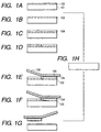
- a production method of semiconductor base material will be described with reference to Figs. 1A to 1H, as an embodiment of the present invention.
- an impurity is introduced into a surface of a single-crystal silicon wafer 101 by a method of thermal diffusion, ion implantation, contamination upon preparation of the wafer, or the like, to form a p + (or n + ) layer 102, at least, in the wafer surface (Fig. 1A).
- the impurity-introduced wafer surface is subjected to anodization, for example, in an HF solution.
- anodization for example, in an HF solution.
- This makes the surface area porous, thereby forming a porous layer 103 (Fig. 1B).
- an epitaxial layer comprised of single-crystal silicon (hereinafter will be referred to as a single-crystal silicon layer) 104 is grown by liquid phase epitaxy on the surface of the porous layer 103 (Fig. 1C).
- the anodization current can be changed, for example, midway from a low level to a high level, to preliminarily provide the structure of the porous layer with difference in density, thereby facilitating the separation of the single-crystal silicon layer 104 from the silicon wafer 101 through the porous layer 103 after the epitaxial growth.
- the single-crystal silicon layer 104 grown on the porous layer 103 is supported through an adhesive 105 by a support member 106 (Fig. 1E). Then the porous layer 103 is broken to separate the single-crystal silicon layer 104 (Figs. 1F and 1G).
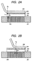
- the silicon wafer is held by vacuum attachment of the surface on the side opposite to the side of the single-crystal silicon layer and the separation is initiated from an area except for the periphery of the substrate, for example, from the center of the substrate (Fig. 1D).
- the separation force Fp and holding force Fv are considered to act, each as illustrated, in the vertical direction in the area around the initial point S.
- reference numeral 207 denotes a substrate holding base and 208 denotes vacuum attaching holes.
- the holding force Fv acts only on the central side of the wafer in the area around the initial point S.
- the even holding force Fv acts in the area around the initial point S, so as to yield a strong holding force. Therefore, even under the holding condition that the lifting of the wafer occurs by the separation from the edge of the wafer, the wafer can be held firmly without lifting by initiating the separation from the area other than the edge.
- the separation can be initiated smoothly from a desired position if a portion of the silicon layer is preliminarily removed, at least, in the separation initiating part.
- the separated region is divided into two areas (Fig. 1D).
- an adhesive is applied onto one area and the support member is bonded thereto (Fig. 1E).
- the separation of the area is effected from the region along the diameter line from which the silicon layer was removed, toward the wafer edge (to the right in the figure) (Fig. 1F).
- the other remaining area is also separated from the wafer in similar fashion, obtaining a thin-film silicon layer (Fig. 1G).
- the silicon layers 104 thus separated are used for the semiconductor base materials or solar cells after the residue of the porous layer 103 is removed as the occasion demands.
- the vacuum attachment and/or electrostatic attachment without damage to the wafer is preferable as a method of supporting the wafer.
- porous layer will be described with an example of silicon.
- a hydrofluoric acid (HF) solution is preferably used in the anodization method for formation of the porous layer 103, a solution of hydrochloric acid, sulfuric acid, or the like can also be used.
- the p + (or n + ) layer 102 can be made porous in the HF concentration of not less than 10%.
- the current flow during the anodization can be properly determined, depending upon the HF concentration, the desired film thickness of the porous layer, the surface condition of the porous layer, or the like, and an appropriate range thereof is approximately 1 mA/cm 2 to 100 mA/cm 2 .
- an alcohol such as ethyl alcohol or the like
- bubbles of reaction product gases evolving during the anodization can be eliminated instantly from the reacting surface without agitation, whereby the porous layer can be formed uniformly and efficiently.
- the amount of the alcohol added is properly determined depending upon the HF concentration, the desired film thickness of the porous layer, or the surface condition of the porous layer, and, particularly, it is necessary to determine the amount of alcohol with such attention as to prevent the HF concentration from becoming too low.
- the density of single-crystal silicon is 2.33 g/cm 3 , but the density of the porous layer can be varied, for example, in the range of 1.1 to 0.6 g/cm 3 , for example, by changing the concentration of the HF solution in the range of 50 to 20%.
- the porosity can also be varied by changing the anodization current, and increasing the current will also increase the porosity.
- the mechanical strength of the porous layer differs depending upon the porosity and is considered to be sufficiently lower than that of the bulk silicon. For example, supposing the porosity is 50%, the mechanical strength can be considered to be half of that of the bulk. If a substrate were bonded to the surface of the porous layer and if sufficient adhesion were present between the porous layer and the substrate, the porous layer would be broken by a compressive, pulling, or shearing force placed between the silicon wafer with the porous layer formed therein, and the substrate. If the porosity is increased further the porous layer will be able to be broken by a weaker force.
- the porous layer is made mainly by the anodization of p-type silicon in which holes are present (T. Unagami, J. Electrochem. Soc., vol. 127, 476 (1980)). There is, however, also a report that the porous layer can be made of low-resistance n-type silicon, on the other hand (R. P. Holmstrom and J. Y. Chi, Appl. Phys. Lett., vol. 42, 386 (1983)). Therefore, the porous layer is considered to be able to be formed of any low-resistance silicon, independent of the conductivity type, i.e., independent of either the p-type or the n-type.
- porous layer it is also possible to effect selective formation of the porous layer depending upon the conductivity type; for example, only the p-type layer can be made porous by anodization in a dark place as in the FIPOS (Full Isolation by Porous Oxidized Silicon) process.
- FIPOS Frull Isolation by Porous Oxidized Silicon
- the porous layer (silicon layer) resulting from anodization of single-crystal silicon has pores of a diameter of about several nm and the density of the porous silicon is not more than half the density of the single-crystal silicon. In spite of this fact, the single-crystallinity is maintained, so that an epitaxial layer can be grown on the porous layer (silicon layer) by thermal CVD, liquid phase growth, or the like.
- the porous layer includes a large amount of voids inside thereof, the surface area thereof is dramatically increased in comparison with the volume. As a result, the chemical etching rate thereof is extremely larger than the etching rates of ordinary single-crystal layers.
- the porous layer can also be obtained similarly by anodization using polycrystal silicon in place of single-crystal silicon.
- a crystal silicon layer can be grown thereon by thermal CVD, liquid phase growth, or the like. (In this case, partial epitaxial growth can be implemented corresponding to the sizes of crystal grains of polycrystal silicon.)
- Boron (B) was introduced by thermal diffusion into one surface of a p-type silicon single-crystal substrate (silicon wafer) 301 having the thickness of 800 ⁇ m and the diameter of 4 inches to form the p + layer.
- This substrate was anodized at two levels of current in a hydrofluoric acid solution to obtain the porous layer 302 in the thickness of about 10 ⁇ m.
- the current was supplied in the density of 8 mA/cm 2 for ten minutes and thereafter in the density of 30 mA/cm 2 for one minute.
- the change of current on the way of the current supply resulted in forming a double-layer structure consisting of a porous layer of dense structure and a porous layer of coarse structure.
- the p-type silicon single-crystal substrate (silicon wafer) 301 with the porous layer 302 formed therein was annealed at the surface temperature of 1050°C in a hydrogen atmosphere for one minute.
- the substrate was immersed in a metal indium solution at 900°C in which silicon was dissolved to a concentration in a supersaturation state.
- the solution was gradually cooled to form the epitaxial layer (hereinafter referred to as a silicon layer) 303 in the thickness of 30 ⁇ m.
- the surface of the substrate 301 on the side opposite to the side of the porous layer 302 was covered by an oxide film so as to repel the solution, whereby the silicon layer 303 was formed only on the surface in which the porous layer was formed.
- solar cells were formed therein.
- the two areas 303-1, 303-2 of 70 ⁇ 34 mm 2 were masked and dry etching by RIE was carried out to remove an appropriate depth of the porous layer from the surface (Fig. 3A).
- the mask was removed and phosphorus (P) was made to diffuse into the surface of each 70 ⁇ 34 mm 2 silicon layer 303 to form the n + layer.
- electrodes 304 and antireflection layers 305 were formed thereon.
- the surface of the substrate 301 on the other side than the solar cell side was held by vacuum attachment and a transparent adhesive 306 was applied onto the surface of the antireflection layer 304 of one silicon layer 303-1 so as not to overflow into the removed portions and removed side surfaces. Then a transparent support member 307 was fixed to the surface and thereafter a force was applied to the porous layer 302 from a part close to the center to separate the silicon layer 303-1 from the silicon substrate 301 (Fig. 3B). A back electrode was formed on the silicon layer, thereby obtaining a thin-film solar cell. Likewise, the remaining silicon layer 303-2 was also treated so as to form the thin-form solar cell. During the separation the thin-film semiconductor layer was able to be separated completely throughout the entire surface without lifting of the wafer.
- the residue of the porous layer was removed by etching from the silicon wafer 301 and the silicon wafer 301 was used repeatedly in totally five processes of the above-stated steps.
- the characteristics of the thin-film solar cells thus obtained were evaluated and it was verified thereby that they demonstrated high efficiency on a stable basis, regardless of the number of uses of the wafer.
- the p + type silicon wafer 401 of the diameter of 5 inches was subjected to the current supply in the density of 8 mA/cm 2 for ten minutes and thereafter in the density of 20 mA/cm 2 for two minutes in a manner similar to that in Example 1, to form the porous layer 402 in the double-layer structure, and thereafter the wafer was subjected to epitaxy on the both surfaces thereof by CVD to form epitaxial layers (silicon semiconductor layers) 403a, 403b each in the thickness of 15 ⁇ m.
- a diffusing agent was applied onto the surface of the epitaxial layer 403a deposited on the porous layer to form the p + layer and thereafter the silicon layer was etched away in the width of 3 mm along the diameter of the wafer in the surface of 403a, thereby dividing the region into two areas 403a-1, 403a-2 (Fig. 4A).
- a solar cell of 4 cm 2 was produced in similar fashion to that in Example 1, on each of the two split areas 403a-1, 403a-2 of the epitaxial layer and thereafter a transparent adhesive 404 was applied onto the surface of one layer 403a-1 so as not to overflow.
- the support member 405 was adhered to the surface. While holding the surface of the layer 403b by electrostatic attachment, a pulling force was applied to the support member to initiate the separation from the etching line (Fig. 4B), thereby obtaining the solar cell.
- the other layer 403a-2 was also separated in similar fashion. At this time, the layer was separated almost throughout the entire surface, without lifting of the wafer. After the residue of the porous layer was removed, the thin-film solar cells thus obtained were stuck to a metal member with an electroconductive adhesive and the characteristics thereof were evaluated.
- the residue of the porous layer was removed from the silicon wafer 401 and the silicon wafer 401 was subjected to totally ten repetitions of the above-stated steps. Since the silicon layers were deposited on the both surfaces in every process, the wafer decrease equivalent to the thickness of the porous layer was compensated for thereby and there occurred no difficulties in handling even after many repetitions of the above steps. The characteristics of the solar cells thus obtained were compared and evaluated and it was verified thereby that they demonstrated stable conversion efficiency, independent of the number of uses of the wafer.
- the p + layer was formed on the 5-inch silicon wafer 501 and thereafter the anodization was carried out by the current supply in the density of 8 mA/cm 2 for ten minutes and thereafter in the density of 25 mA/cm 2 for one minute to form the porous layer 502 of the double-layer structure in the thickness of about 12 ⁇ m. Then the semiconductor layer was epitaxially grown in the thickness of 0.5 ⁇ m on the porous layer and thereafter P (phosphorus) was made to diffuse thereinto to form the n + layer 503. Further, an epitaxial layer (single-crystal semiconductor layer) 504 was deposited in the thickness of 30 ⁇ m by liquid phase growth.
- a resist mask was formed in the square shape of 80 mm x 80 mm in the central part of the wafer and dry etching by RIE was effected to remove the epitaxial layers (hereinafter referred to as silicon layers) (Fig. 5A). Then, the resist was removed, and at the same time as thermal welding of a metal member 505 to the remaining silicon layer 504 with an Al foil, Al atoms were made to diffuse into the bonding surface of the silicon layer 504 to form the p + layer. After that, the back surface was held by a combination of vacuum attachment and electrostatic attachment, and a force was applied to the porous layer 502 to obtain a thin film.
- the separation was initiated from a position about 2 cm closer to the center from the edge of the wafer, so that the separation was implemented without lifting of the wafer.
- the residue of the porous layer remaining on the surface of the thin-film semiconductor layer was removed and a grid electrode was formed thereon.
- an antireflection film of TiO 2 also having the passivation effect was deposited thereon to form a solar cell of 4 cm 2 and the solar cell was evaluated.
- the residue of the porous layer was etched away from the wafer after the separation of the thin film, and the wafer was subjected to totally five repetitions of the above-stated steps.
- the solar cells thus obtained were compared and evaluated, and it was verified thereby that they demonstrated stable efficiency, regardless of the number of uses of the wafer.
Landscapes
- Engineering & Computer Science (AREA)
- Physics & Mathematics (AREA)
- Condensed Matter Physics & Semiconductors (AREA)
- General Physics & Mathematics (AREA)
- Manufacturing & Machinery (AREA)
- Computer Hardware Design (AREA)
- Microelectronics & Electronic Packaging (AREA)
- Power Engineering (AREA)
- Photovoltaic Devices (AREA)
- Recrystallisation Techniques (AREA)
- Crystals, And After-Treatments Of Crystals (AREA)
Applications Claiming Priority (2)
| Application Number | Priority Date | Filing Date | Title |
|---|---|---|---|
| JP11171135A JP2001007362A (ja) | 1999-06-17 | 1999-06-17 | 半導体基材および太陽電池の製造方法 |
| JP17113599 | 1999-06-17 |
Publications (2)
| Publication Number | Publication Date |
|---|---|
| EP1061566A2 true EP1061566A2 (de) | 2000-12-20 |
| EP1061566A3 EP1061566A3 (de) | 2007-01-31 |
Family
ID=15917644
Family Applications (1)
| Application Number | Title | Priority Date | Filing Date |
|---|---|---|---|
| EP00112604A Withdrawn EP1061566A3 (de) | 1999-06-17 | 2000-06-14 | Verfahren zur Herstellung von Halbleiter-Dünnschichten mittels eines Trennschrittes und Solarzellen-Herstellungsverfahren |
Country Status (4)
| Country | Link |
|---|---|
| US (1) | US6448155B1 (de) |
| EP (1) | EP1061566A3 (de) |
| JP (1) | JP2001007362A (de) |
| CN (1) | CN1146957C (de) |
Cited By (5)
| Publication number | Priority date | Publication date | Assignee | Title |
|---|---|---|---|---|
| WO2004008526A1 (en) * | 2002-07-17 | 2004-01-22 | S.O.I.Tec Silicon On Insulator Technologies | A layer transfer method |
| EP1463094A2 (de) * | 2003-03-26 | 2004-09-29 | Lintec Corporation | Vorrichtung zur Herstellung von Halbleitern und Verfahren zur Herstellung von Halbleitereinrichtungen |
| US6972215B2 (en) * | 2001-01-31 | 2005-12-06 | Canon Kabushiki Kaisha | Thin-film semiconductor device and method of manufacturing the same |
| US7029950B2 (en) | 2001-01-31 | 2006-04-18 | Canon Kabushiki Kaisha | Thin-film semiconductor device and method of manufacturing the same |
| EP2269230A4 (de) * | 2008-03-08 | 2016-03-30 | Crystal Solar Inc | Integriertes verfahren und system zur herstellung von monolithischen panels aus kristallinen solarzellen |
Families Citing this family (71)
| Publication number | Priority date | Publication date | Assignee | Title |
|---|---|---|---|---|
| JP2002075917A (ja) * | 2000-08-25 | 2002-03-15 | Canon Inc | 試料の分離装置及び分離方法 |
| JP3697214B2 (ja) * | 2001-03-16 | 2005-09-21 | キヤノン株式会社 | 半導体膜の製造方法 |
| JP2002289536A (ja) * | 2001-03-27 | 2002-10-04 | Sony Corp | 熱cvd装置および薄膜半導体素子の製造方法 |
| JP4266106B2 (ja) * | 2001-09-27 | 2009-05-20 | 株式会社東芝 | 粘着性テープの剥離装置、粘着性テープの剥離方法、半導体チップのピックアップ装置、半導体チップのピックアップ方法及び半導体装置の製造方法 |
| US6616854B2 (en) * | 2001-12-17 | 2003-09-09 | Motorola, Inc. | Method of bonding and transferring a material to form a semiconductor device |
| FR2850390B1 (fr) * | 2003-01-24 | 2006-07-14 | Soitec Silicon On Insulator | Procede d'elimination d'une zone peripherique de colle lors de la fabrication d'un substrat composite |
| US7122095B2 (en) * | 2003-03-14 | 2006-10-17 | S.O.I.Tec Silicon On Insulator Technologies S.A. | Methods for forming an assembly for transfer of a useful layer |
| AU2003902270A0 (en) * | 2003-05-09 | 2003-05-29 | Origin Energy Solar Pty Ltd | Separating and assembling semiconductor strips |
| JP4438049B2 (ja) * | 2003-08-11 | 2010-03-24 | キヤノン株式会社 | 電界効果トランジスタ及びそれを用いたセンサ並びにその製造方法 |
| CN100359393C (zh) * | 2003-12-17 | 2008-01-02 | Lg.菲利浦Lcd株式会社 | 液晶分配装置 |
| JP2005210062A (ja) * | 2003-12-26 | 2005-08-04 | Canon Inc | 半導体部材とその製造方法、及び半導体装置 |
| CN100347837C (zh) * | 2004-07-21 | 2007-11-07 | 宏齐科技股份有限公司 | 半导体基材构造及其加工方法 |
| US9508886B2 (en) | 2007-10-06 | 2016-11-29 | Solexel, Inc. | Method for making a crystalline silicon solar cell substrate utilizing flat top laser beam |
| US8399331B2 (en) | 2007-10-06 | 2013-03-19 | Solexel | Laser processing for high-efficiency thin crystalline silicon solar cell fabrication |
| US8420435B2 (en) * | 2009-05-05 | 2013-04-16 | Solexel, Inc. | Ion implantation fabrication process for thin-film crystalline silicon solar cells |
| US8129822B2 (en) * | 2006-10-09 | 2012-03-06 | Solexel, Inc. | Template for three-dimensional thin-film solar cell manufacturing and methods of use |
| US20090107545A1 (en) * | 2006-10-09 | 2009-04-30 | Soltaix, Inc. | Template for pyramidal three-dimensional thin-film solar cell manufacturing and methods of use |
| US9362439B2 (en) * | 2008-05-07 | 2016-06-07 | Silicon Genesis Corporation | Layer transfer of films utilizing controlled shear region |
| US20100304521A1 (en) * | 2006-10-09 | 2010-12-02 | Solexel, Inc. | Shadow Mask Methods For Manufacturing Three-Dimensional Thin-Film Solar Cells |
| US8035028B2 (en) * | 2006-10-09 | 2011-10-11 | Solexel, Inc. | Pyramidal three-dimensional thin-film solar cells |
| US20080264477A1 (en) * | 2006-10-09 | 2008-10-30 | Soltaix, Inc. | Methods for manufacturing three-dimensional thin-film solar cells |
| US8512581B2 (en) * | 2006-10-09 | 2013-08-20 | Solexel, Inc. | Methods for liquid transfer coating of three-dimensional substrates |
| US7999174B2 (en) * | 2006-10-09 | 2011-08-16 | Solexel, Inc. | Solar module structures and assembly methods for three-dimensional thin-film solar cells |
| US8193076B2 (en) | 2006-10-09 | 2012-06-05 | Solexel, Inc. | Method for releasing a thin semiconductor substrate from a reusable template |
| US8293558B2 (en) * | 2006-10-09 | 2012-10-23 | Solexel, Inc. | Method for releasing a thin-film substrate |
| US8322300B2 (en) * | 2008-02-07 | 2012-12-04 | Sunpower Corporation | Edge coating apparatus with movable roller applicator for solar cell substrates |
| US8662008B2 (en) * | 2008-02-07 | 2014-03-04 | Sunpower Corporation | Edge coating apparatus for solar cell substrates |
| US20100144080A1 (en) * | 2008-06-02 | 2010-06-10 | Solexel, Inc. | Method and apparatus to transfer coat uneven surface |
| US8288195B2 (en) * | 2008-11-13 | 2012-10-16 | Solexel, Inc. | Method for fabricating a three-dimensional thin-film semiconductor substrate from a template |
| US8294026B2 (en) | 2008-11-13 | 2012-10-23 | Solexel, Inc. | High-efficiency thin-film solar cells |
| MY160251A (en) * | 2008-11-26 | 2017-02-28 | Solexel Inc | Truncated pyramid -structures for see-through solar cells |
| US8906218B2 (en) | 2010-05-05 | 2014-12-09 | Solexel, Inc. | Apparatus and methods for uniformly forming porous semiconductor on a substrate |
| US9076642B2 (en) | 2009-01-15 | 2015-07-07 | Solexel, Inc. | High-Throughput batch porous silicon manufacturing equipment design and processing methods |
| MY170119A (en) * | 2009-01-15 | 2019-07-05 | Trutag Tech Inc | Porous silicon electro-etching system and method |
| US9343299B2 (en) * | 2009-02-06 | 2016-05-17 | Solexel, Inc. | Trench formation method for releasing a substrate from a semiconductor template |
| MY162405A (en) * | 2009-02-06 | 2017-06-15 | Solexel Inc | Trench Formation Method For Releasing A Thin-Film Substrate From A Reusable Semiconductor Template |
| US8828517B2 (en) | 2009-03-23 | 2014-09-09 | Solexel, Inc. | Structure and method for improving solar cell efficiency and mechanical strength |
| WO2010120850A1 (en) * | 2009-04-14 | 2010-10-21 | Solexel, Inc. | High efficiency epitaxial chemical vapor deposition (cvd) reactor |
| US9099584B2 (en) * | 2009-04-24 | 2015-08-04 | Solexel, Inc. | Integrated three-dimensional and planar metallization structure for thin film solar cells |
| US9318644B2 (en) | 2009-05-05 | 2016-04-19 | Solexel, Inc. | Ion implantation and annealing for thin film crystalline solar cells |
| EP2427914A4 (de) | 2009-05-05 | 2013-06-05 | Solexel Inc | Hochproduktionsanlage zur herstellung poröser halbleiter |
| US8445314B2 (en) * | 2009-05-22 | 2013-05-21 | Solexel, Inc. | Method of creating reusable template for detachable thin film substrate |
| EP2436028B1 (de) * | 2009-05-29 | 2016-08-10 | Solexel, Inc. | Durchsichtiges dreidimensionales dünnfilmsolarzelle-halbleitersubstrat und herstellungsverfahren dafür |
| EP2510551B1 (de) | 2009-12-09 | 2017-08-02 | Solexel, Inc. | Herstellungsverfahren von Solarzellen mit Rückseitenkontakten und Rückseitenübergang |
| WO2011100647A2 (en) | 2010-02-12 | 2011-08-18 | Solexel, Inc. | Double-sided reusable template for fabrication of semiconductor substrates for photovoltaic cell and microelectronics device manufacturing |
| WO2011156657A2 (en) | 2010-06-09 | 2011-12-15 | Solexel, Inc. | High productivity thin film deposition method and system |
| JP5902406B2 (ja) * | 2010-06-25 | 2016-04-13 | 株式会社半導体エネルギー研究所 | 分離方法および半導体装置の作製方法 |
| MY158500A (en) | 2010-08-05 | 2016-10-14 | Solexel Inc | Backplane reinforcement and interconnects for solar cells |
| CN102560636B (zh) * | 2010-12-14 | 2016-03-30 | 北京北方微电子基地设备工艺研究中心有限责任公司 | 一种基片承载装置及应用该装置的基片处理设备 |
| US9748414B2 (en) | 2011-05-20 | 2017-08-29 | Arthur R. Zingher | Self-activated front surface bias for a solar cell |
| CN103258716B (zh) | 2012-02-16 | 2016-03-09 | 财团法人工业技术研究院 | 制作具有织化表面的半导体层的方法、制作太阳能电池的方法 |
| US8895347B2 (en) | 2012-02-16 | 2014-11-25 | Industrial Technology Research Institute | Method for fabricating semiconductor layer having textured surface and method for fabricating solar cell |
| US9437756B2 (en) | 2013-09-27 | 2016-09-06 | Sunpower Corporation | Metallization of solar cells using metal foils |
| US9653638B2 (en) | 2013-12-20 | 2017-05-16 | Sunpower Corporation | Contacts for solar cells formed by directing a laser beam with a particular shape on a metal foil over a dielectric region |
| US9178104B2 (en) | 2013-12-20 | 2015-11-03 | Sunpower Corporation | Single-step metal bond and contact formation for solar cells |
| US9947812B2 (en) | 2014-03-28 | 2018-04-17 | Sunpower Corporation | Metallization of solar cells |
| US9231129B2 (en) | 2014-03-28 | 2016-01-05 | Sunpower Corporation | Foil-based metallization of solar cells |
| US9620661B2 (en) | 2014-12-19 | 2017-04-11 | Sunpower Corporation | Laser beam shaping for foil-based metallization of solar cells |
| US20160380127A1 (en) | 2015-06-26 | 2016-12-29 | Richard Hamilton SEWELL | Leave-In Etch Mask for Foil-Based Metallization of Solar Cells |
| US9620655B1 (en) | 2015-10-29 | 2017-04-11 | Sunpower Corporation | Laser foil trim approaches for foil-based metallization for solar cells |
| US11424373B2 (en) | 2016-04-01 | 2022-08-23 | Sunpower Corporation | Thermocompression bonding approaches for foil-based metallization of non-metal surfaces of solar cells |
| US10290763B2 (en) | 2016-05-13 | 2019-05-14 | Sunpower Corporation | Roll-to-roll metallization of solar cells |
| US9882071B2 (en) | 2016-07-01 | 2018-01-30 | Sunpower Corporation | Laser techniques for foil-based metallization of solar cells |
| US10115855B2 (en) | 2016-09-30 | 2018-10-30 | Sunpower Corporation | Conductive foil based metallization of solar cells |
| US11908958B2 (en) | 2016-12-30 | 2024-02-20 | Maxeon Solar Pte. Ltd. | Metallization structures for solar cells |
| WO2019195804A1 (en) | 2018-04-06 | 2019-10-10 | Sunpower Corporation | Laser assisted metallization process for solar cell circuit formation |
| US11276785B2 (en) | 2018-04-06 | 2022-03-15 | Sunpower Corporation | Laser assisted metallization process for solar cell fabrication |
| WO2019195806A2 (en) | 2018-04-06 | 2019-10-10 | Sunpower Corporation | Local patterning and metallization of semiconductor structures using a laser beam |
| US11664472B2 (en) | 2018-04-06 | 2023-05-30 | Maxeon Solar Pte. Ltd. | Laser assisted metallization process for solar cell stringing |
| CN112119508A (zh) | 2018-04-06 | 2020-12-22 | 太阳能公司 | 用于太阳能电池串接的激光辅助金属化工艺 |
| CN113299576B (zh) * | 2020-02-21 | 2022-11-22 | 济南晶正电子科技有限公司 | 一种薄膜机械分离装置 |
Citations (3)
| Publication number | Priority date | Publication date | Assignee | Title |
|---|---|---|---|---|
| EP0851513A2 (de) * | 1996-12-27 | 1998-07-01 | Canon Kabushiki Kaisha | Herstellungsverfahren eines Halbleiter-Bauelements und Herstellungsverfahren einer Solarzelle |
| US5811348A (en) * | 1995-02-02 | 1998-09-22 | Sony Corporation | Method for separating a device-forming layer from a base body |
| JPH10270728A (ja) * | 1997-03-25 | 1998-10-09 | Sony Corp | 薄膜半導体および半導体装置の製造方法 |
Family Cites Families (6)
| Publication number | Priority date | Publication date | Assignee | Title |
|---|---|---|---|---|
| JP3257580B2 (ja) | 1994-03-10 | 2002-02-18 | キヤノン株式会社 | 半導体基板の作製方法 |
| JPH09331049A (ja) * | 1996-04-08 | 1997-12-22 | Canon Inc | 貼り合わせsoi基板の作製方法及びsoi基板 |
| SG55413A1 (en) * | 1996-11-15 | 1998-12-21 | Method Of Manufacturing Semico | Method of manufacturing semiconductor article |
| JP3647176B2 (ja) | 1996-12-27 | 2005-05-11 | キヤノン株式会社 | 半導体基材及び太陽電池の製造方法及びその製造装置 |
| JP3501606B2 (ja) | 1996-12-27 | 2004-03-02 | キヤノン株式会社 | 半導体基材の製造方法、および太陽電池の製造方法 |
| US6143628A (en) * | 1997-03-27 | 2000-11-07 | Canon Kabushiki Kaisha | Semiconductor substrate and method of manufacturing the same |
-
1999
- 1999-06-17 JP JP11171135A patent/JP2001007362A/ja active Pending
-
2000
- 2000-06-12 US US09/592,559 patent/US6448155B1/en not_active Expired - Fee Related
- 2000-06-14 EP EP00112604A patent/EP1061566A3/de not_active Withdrawn
- 2000-06-16 CN CNB001225898A patent/CN1146957C/zh not_active Expired - Fee Related
Patent Citations (3)
| Publication number | Priority date | Publication date | Assignee | Title |
|---|---|---|---|---|
| US5811348A (en) * | 1995-02-02 | 1998-09-22 | Sony Corporation | Method for separating a device-forming layer from a base body |
| EP0851513A2 (de) * | 1996-12-27 | 1998-07-01 | Canon Kabushiki Kaisha | Herstellungsverfahren eines Halbleiter-Bauelements und Herstellungsverfahren einer Solarzelle |
| JPH10270728A (ja) * | 1997-03-25 | 1998-10-09 | Sony Corp | 薄膜半導体および半導体装置の製造方法 |
Cited By (9)
| Publication number | Priority date | Publication date | Assignee | Title |
|---|---|---|---|---|
| US6972215B2 (en) * | 2001-01-31 | 2005-12-06 | Canon Kabushiki Kaisha | Thin-film semiconductor device and method of manufacturing the same |
| US7029950B2 (en) | 2001-01-31 | 2006-04-18 | Canon Kabushiki Kaisha | Thin-film semiconductor device and method of manufacturing the same |
| WO2004008526A1 (en) * | 2002-07-17 | 2004-01-22 | S.O.I.Tec Silicon On Insulator Technologies | A layer transfer method |
| FR2842647A1 (fr) * | 2002-07-17 | 2004-01-23 | Soitec Silicon On Insulator | Procede de transfert de couche |
| US6913971B2 (en) | 2002-07-17 | 2005-07-05 | S.O.I. Tec Silicon On Insulator Technologies S.A. | Layer transfer methods |
| EP1463094A2 (de) * | 2003-03-26 | 2004-09-29 | Lintec Corporation | Vorrichtung zur Herstellung von Halbleitern und Verfahren zur Herstellung von Halbleitereinrichtungen |
| EP1463094A3 (de) * | 2003-03-26 | 2006-11-02 | Lintec Corporation | Vorrichtung zur Herstellung von Halbleitern und Verfahren zur Herstellung von Halbleitereinrichtungen |
| US7223319B2 (en) | 2003-03-26 | 2007-05-29 | Kabushiki Kaisha Toshiba | Semiconductor manufacturing apparatus and method of manufacturing semiconductor device |
| EP2269230A4 (de) * | 2008-03-08 | 2016-03-30 | Crystal Solar Inc | Integriertes verfahren und system zur herstellung von monolithischen panels aus kristallinen solarzellen |
Also Published As
| Publication number | Publication date |
|---|---|
| CN1146957C (zh) | 2004-04-21 |
| JP2001007362A (ja) | 2001-01-12 |
| EP1061566A3 (de) | 2007-01-31 |
| US6448155B1 (en) | 2002-09-10 |
| CN1278656A (zh) | 2001-01-03 |
Similar Documents
| Publication | Publication Date | Title |
|---|---|---|
| US6448155B1 (en) | Production method of semiconductor base material and production method of solar cell | |
| KR100300279B1 (ko) | 반도체기판의제조방법 | |
| US6664169B1 (en) | Process for producing semiconductor member, process for producing solar cell, and anodizing apparatus | |
| US7022585B2 (en) | Method for making thin film devices intended for solar cells or silicon-on-insulator (SOI) applications | |
| CA2225131C (en) | Process for producing semiconductor article | |
| KR100395077B1 (ko) | 복합부재의 분리방법 및 박막제작방법 | |
| US7148119B1 (en) | Process for production of semiconductor substrate | |
| US6569748B1 (en) | Substrate and production method thereof | |
| CA2198552C (en) | Fabrication process of semiconductor substrate | |
| EP0867923B1 (de) | Verfahren zur Trennung einer Schicht | |
| KR19980042474A (ko) | 반도체물품의 제조방법 | |
| JP2001094136A (ja) | 半導体素子モジュールの製造方法および太陽電池モジュールの製造方法 | |
| US6417069B1 (en) | Substrate processing method and manufacturing method, and anodizing apparatus | |
| JP3472197B2 (ja) | 半導体基材及び太陽電池の製造方法 | |
| JP4035862B2 (ja) | 半導体基板の製造方法 | |
| JPH10326883A (ja) | 基板及びその作製方法 | |
| JP3297600B2 (ja) | 半導体基板の作製方法 | |
| EP1385200B1 (de) | Verfahren zur Herstellung von Dünnschichtbauelementen für Solarzellen oder SOI-Anwendungen | |
| JPH10270670A (ja) | 薄膜半導体の製造方法 | |
| JP3293766B2 (ja) | 半導体部材の製造方法 | |
| JP2000277403A (ja) | 半導体基体の作製方法 | |
| JP2000223725A (ja) | 光電変換装置および半導体層の分離方法 |
Legal Events
| Date | Code | Title | Description |
|---|---|---|---|
| PUAI | Public reference made under article 153(3) epc to a published international application that has entered the european phase |
Free format text: ORIGINAL CODE: 0009012 |
|
| AK | Designated contracting states |
Kind code of ref document: A2 Designated state(s): AT BE CH CY DE DK ES FI FR GB GR IE IT LI LU MC NL PT SE |
|
| AX | Request for extension of the european patent |
Free format text: AL;LT;LV;MK;RO;SI |
|
| PUAL | Search report despatched |
Free format text: ORIGINAL CODE: 0009013 |
|
| AK | Designated contracting states |
Kind code of ref document: A3 Designated state(s): AT BE CH CY DE DK ES FI FR GB GR IE IT LI LU MC NL PT SE |
|
| AX | Request for extension of the european patent |
Extension state: AL LT LV MK RO SI |
|
| 17P | Request for examination filed |
Effective date: 20070731 |
|
| AKX | Designation fees paid |
Designated state(s): AT BE CH CY DE DK ES FI FR GB GR IE IT LI LU MC NL PT SE |
|
| 17Q | First examination report despatched |
Effective date: 20071011 |
|
| STAA | Information on the status of an ep patent application or granted ep patent |
Free format text: STATUS: THE APPLICATION HAS BEEN WITHDRAWN |
|
| 18W | Application withdrawn |
Effective date: 20071212 |