EP1051657B1 - Color filter layer of cholesterically ordered material, and reflective lcd provided with such a color filter layer - Google Patents
Color filter layer of cholesterically ordered material, and reflective lcd provided with such a color filter layer Download PDFInfo
- Publication number
- EP1051657B1 EP1051657B1 EP99960991A EP99960991A EP1051657B1 EP 1051657 B1 EP1051657 B1 EP 1051657B1 EP 99960991 A EP99960991 A EP 99960991A EP 99960991 A EP99960991 A EP 99960991A EP 1051657 B1 EP1051657 B1 EP 1051657B1
- Authority
- EP
- European Patent Office
- Prior art keywords
- color filter
- filter layer
- layer
- color
- dyes
- Prior art date
- Legal status (The legal status is an assumption and is not a legal conclusion. Google has not performed a legal analysis and makes no representation as to the accuracy of the status listed.)
- Expired - Lifetime
Links
- 239000000463 material Substances 0.000 title claims abstract description 40
- 239000000975 dye Substances 0.000 claims abstract description 50
- 239000004973 liquid crystal related substance Substances 0.000 claims abstract description 14
- 239000003086 colorant Substances 0.000 claims abstract description 10
- 239000000758 substrate Substances 0.000 claims description 22
- 230000003098 cholesteric effect Effects 0.000 claims description 14
- 238000010521 absorption reaction Methods 0.000 claims description 13
- 239000007788 liquid Substances 0.000 claims description 11
- 239000002178 crystalline material Substances 0.000 claims description 9
- 239000000126 substance Substances 0.000 claims description 7
- 229920000642 polymer Polymers 0.000 claims description 5
- 239000010410 layer Substances 0.000 description 113
- 238000001228 spectrum Methods 0.000 description 8
- 239000000203 mixture Substances 0.000 description 7
- 150000001875 compounds Chemical class 0.000 description 6
- 230000010287 polarization Effects 0.000 description 6
- 230000001419 dependent effect Effects 0.000 description 4
- 239000011521 glass Substances 0.000 description 4
- KFZMGEQAYNKOFK-UHFFFAOYSA-N Isopropanol Chemical compound CC(C)O KFZMGEQAYNKOFK-UHFFFAOYSA-N 0.000 description 3
- 239000004642 Polyimide Substances 0.000 description 3
- 238000000862 absorption spectrum Methods 0.000 description 3
- 229920001721 polyimide Polymers 0.000 description 3
- 150000001252 acrylic acid derivatives Chemical class 0.000 description 2
- 230000002349 favourable effect Effects 0.000 description 2
- 238000004519 manufacturing process Methods 0.000 description 2
- 239000011159 matrix material Substances 0.000 description 2
- 238000000034 method Methods 0.000 description 2
- KWVGIHKZDCUPEU-UHFFFAOYSA-N 2,2-dimethoxy-2-phenylacetophenone Chemical compound C=1C=CC=CC=1C(OC)(OC)C(=O)C1=CC=CC=C1 KWVGIHKZDCUPEU-UHFFFAOYSA-N 0.000 description 1
- OWYWGLHRNBIFJP-UHFFFAOYSA-N Ipazine Chemical compound CCN(CC)C1=NC(Cl)=NC(NC(C)C)=N1 OWYWGLHRNBIFJP-UHFFFAOYSA-N 0.000 description 1
- 230000005540 biological transmission Effects 0.000 description 1
- 239000011247 coating layer Substances 0.000 description 1
- 125000004386 diacrylate group Chemical group 0.000 description 1
- 239000002019 doping agent Substances 0.000 description 1
- 230000005684 electric field Effects 0.000 description 1
- 238000005265 energy consumption Methods 0.000 description 1
- 238000007496 glass forming Methods 0.000 description 1
- 239000004922 lacquer Substances 0.000 description 1
- 239000002184 metal Substances 0.000 description 1
- 239000000178 monomer Substances 0.000 description 1
- NWVVVBRKAWDGAB-UHFFFAOYSA-N p-methoxyphenol Chemical compound COC1=CC=C(O)C=C1 NWVVVBRKAWDGAB-UHFFFAOYSA-N 0.000 description 1
- 238000005191 phase separation Methods 0.000 description 1
- 239000000049 pigment Substances 0.000 description 1
- 239000002861 polymer material Substances 0.000 description 1
- 238000006116 polymerization reaction Methods 0.000 description 1
- 238000000926 separation method Methods 0.000 description 1
- 238000004528 spin coating Methods 0.000 description 1
- 238000004544 sputter deposition Methods 0.000 description 1
- 230000006641 stabilisation Effects 0.000 description 1
- 238000011105 stabilization Methods 0.000 description 1
- 239000003381 stabilizer Substances 0.000 description 1
- 229920002994 synthetic fiber Polymers 0.000 description 1
- 239000012780 transparent material Substances 0.000 description 1
Images

Classifications
-
- G—PHYSICS
- G02—OPTICS
- G02F—OPTICAL DEVICES OR ARRANGEMENTS FOR THE CONTROL OF LIGHT BY MODIFICATION OF THE OPTICAL PROPERTIES OF THE MEDIA OF THE ELEMENTS INVOLVED THEREIN; NON-LINEAR OPTICS; FREQUENCY-CHANGING OF LIGHT; OPTICAL LOGIC ELEMENTS; OPTICAL ANALOGUE/DIGITAL CONVERTERS
- G02F1/00—Devices or arrangements for the control of the intensity, colour, phase, polarisation or direction of light arriving from an independent light source, e.g. switching, gating or modulating; Non-linear optics
- G02F1/01—Devices or arrangements for the control of the intensity, colour, phase, polarisation or direction of light arriving from an independent light source, e.g. switching, gating or modulating; Non-linear optics for the control of the intensity, phase, polarisation or colour
- G02F1/13—Devices or arrangements for the control of the intensity, colour, phase, polarisation or direction of light arriving from an independent light source, e.g. switching, gating or modulating; Non-linear optics for the control of the intensity, phase, polarisation or colour based on liquid crystals, e.g. single liquid crystal display cells
- G02F1/133—Constructional arrangements; Operation of liquid crystal cells; Circuit arrangements
- G02F1/1333—Constructional arrangements; Manufacturing methods
- G02F1/1335—Structural association of cells with optical devices, e.g. polarisers or reflectors
- G02F1/133509—Filters, e.g. light shielding masks
- G02F1/133514—Colour filters
- G02F1/133516—Methods for their manufacture, e.g. printing, electro-deposition or photolithography
-
- G—PHYSICS
- G02—OPTICS
- G02B—OPTICAL ELEMENTS, SYSTEMS OR APPARATUS
- G02B5/00—Optical elements other than lenses
- G02B5/30—Polarising elements
- G02B5/3016—Polarising elements involving passive liquid crystal elements
-
- G—PHYSICS
- G02—OPTICS
- G02F—OPTICAL DEVICES OR ARRANGEMENTS FOR THE CONTROL OF LIGHT BY MODIFICATION OF THE OPTICAL PROPERTIES OF THE MEDIA OF THE ELEMENTS INVOLVED THEREIN; NON-LINEAR OPTICS; FREQUENCY-CHANGING OF LIGHT; OPTICAL LOGIC ELEMENTS; OPTICAL ANALOGUE/DIGITAL CONVERTERS
- G02F1/00—Devices or arrangements for the control of the intensity, colour, phase, polarisation or direction of light arriving from an independent light source, e.g. switching, gating or modulating; Non-linear optics
- G02F1/01—Devices or arrangements for the control of the intensity, colour, phase, polarisation or direction of light arriving from an independent light source, e.g. switching, gating or modulating; Non-linear optics for the control of the intensity, phase, polarisation or colour
- G02F1/13—Devices or arrangements for the control of the intensity, colour, phase, polarisation or direction of light arriving from an independent light source, e.g. switching, gating or modulating; Non-linear optics for the control of the intensity, phase, polarisation or colour based on liquid crystals, e.g. single liquid crystal display cells
- G02F1/133—Constructional arrangements; Operation of liquid crystal cells; Circuit arrangements
- G02F1/1333—Constructional arrangements; Manufacturing methods
- G02F1/1335—Structural association of cells with optical devices, e.g. polarisers or reflectors
- G02F1/133553—Reflecting elements
Definitions
- the invention relates to a color filter layer of a cholesterically ordered material, in which the axis of the molecular helix of the cholesterically ordered material extends transversely to the layer.
- the invention also relates to a liquid crystal color display device of the reflective type, provided with such a color filter layer.
- Color filter layers also referred to as cholesteric mirrors, are known per se. They comprise a relatively thin layer of a liquid crystalline material having a cholesteric (or chirally nematic) order.
- the liquid crystalline molecules of this material have such a structure that they order to a spiral or helix-like structure in a solution -spontaneously or under the influence of given doping agents. After such a solution has been provided between two parallel substrates, this helix-like structure is aligned in such a way that the axis of the molecular helix extends transversely to the layer thus obtained. A better alignment of the helix is obtained if an orientation layer is provided on the facing surfaces of the substrates.
- Such a color filter layer When unpolarized light is incident on such a color filter layer, that part of the light which "fits" the (dextrorotatory or levorotatory) direction and pitch of the helix is reflected, whereas the rest of the incident light is transmitted. If desired, this transmitted light is absorbed on an absorption layer which is present behind the color filter layer.
- the (reflected) color of the layer is mainly determined by the pitch of the cholesterically ordered material.
- Such filter layers may be used as coating layers or as mirror layers, for example for decorative purposes.
- color filter layer of the type described in the opening paragraph which, according to the invention, is characterized in that the color filter layer comprises at least one or more dyes which absorb unwanted colors caused by color shifts.
- the dye(s) should therefore preferably be chosen to be such that its (their) absorption wavelength(s) correspond(s) to the wavelength(s) of the unwanted color(s).
- the absorption band of both dyes should have at least some overlap with both edges of the reflection band of the cholesterically ordered material.
- a filter of this type has the important advantage that also the intensity of the color does not have any angle dependence. It will be evident that in this case a single dye having two or more absorption bands may also be used.
- a favorable embodiment of the color filter layer according to the invention is characterized in that the cholesterically ordered material comprises a polymer network.
- a network consists of a polymer material having a three-dimensional structure. At least a part of the liquid crystalline molecules present in the layer is preferably incorporated in the network. The presence of such a network causes the reflection characteristic of the color filter to be relatively insensitive to mechanical tensions and temperature changes.
- a further preferred embodiment of the color filter layer according to the invention is characterized in that the pitch of the molecular helix is varied in such a way that the difference between the maximum pitch and the minimum pitch is at least 20 nm.
- Cholesteric color filter layers ordered in such a way have a relatively broad reflection band which, dependent on the refractive indices of the layer, may have a width of 80 nm or more. The possibility of adjusting the width of the reflection band provides great advantages in the eventual color setting of the color filter.
- the pitch difference is preferably 50 nm or more.
- a further preferred embodiment of the color filter layer according to the invention is characterized in that the dye(s) is (are) incorporated in the network via chemical bonds. This measure promotes the stability and durability of the color filter layer according to the invention. Separating one or more of the dyes from the cholesterically ordered layer (for example, by phase separation) is thereby inhibited.
- the invention also relates to a liquid crystal color display device of the reflective type, provided with such a color filter layer. More particularly, the invention relates to a liquid crystal color display device of the reflective type, comprising two substantially parallel substrates provided with an electrode layer and an orientation layer between which a layer of liquid crystalline material is present, one substrate being provided with a broadband absorption layer, a patterned color filter layer of cholesterically ordered material, and a 1/4 ⁇ layer, and the other substrate being provided with a polarizer.
- FIG. 3 and 4 of European patent application EP-A 600 349 show two such display devices.
- display devices of the reflective type do not require any backlight. Consequently, the reflective display devices have a relatively low energy consumption.
- a liquid crystal color display device of the reflective type with a cholesteric color filter is based on the following principle.
- An incident ray of light of unpolarized white light is polarized by the polarizer to linearly polarized light and is subsequently incident on a pixel of the LC material. If this pixel is not driven by means of an electric voltage, the light ray passes through the LC material and its direction of polarization is rotated, for example 90°. Subsequently, upon passing through the 1/4 ⁇ layer behind this material, it is converted into levo-circularly polarized light.
- this polarized light having a wavelength outside the reflection band of the color filter layer of the ordered cholesteric material completely passes through the color filter layer and is absorbed in the broadband absorption layer.
- the part of the light having a wavelength within the reflection band of the color filter layer is, however, completely reflected on the color filter layer.
- the direction of polarization is converted again into levo linearly polarized light.
- the direction of polarization of the light ray is again rotated in the layer of LC material, for example 90° again, but now in the opposite direction so that the total rotation is 0°.
- this light ray has the correct direction of polarization for passing through the polarizer.
- the color filter layer consists of a pattern of three types of pixels associated with cholesteric materials having different reflection bands. It is possible to manufacture liquid crystal color display devices of the reflective type with such filters.
- the direction of polarization of the linearly polarized light is not rotated in the LC material.
- the direction of polarization is now converted into dextro-circularly polarized light.
- the color filter reflects exclusively levo-circularly polanzed light of a given wavelength.
- the presented dextro-circularly polarized light is fully passed and absorbed in the absorption layer so that nothing of this light reaches the viewer. The viewer thus "sees" a black pixel.
- Liquid crystal color display devices of the reflective type have a major drawback. When watching such display devices, color shifts soon take place if a viewer does not watch the device from a substantially perpendicular direction.
- liquid crystal color display device of the reflective type as mentioned in the opening paragraph, and is characterized in that the color filter layer also comprises one or more dyes which absorb unwanted colors caused by color shifts.
- the invention is based on the recognition that the presence of dyes in or near the color filter layer can absorb the unwanted colors leaving the device at an oblique angle. It has been found that, if the device is viewed at an oblique angle, the wavelength of the relevant pixel shifts to a smaller wavelength. By suitable choice of the bandwidth of the primary colors from the color filter layer and the dyes, the problem of unwanted color shift is alleviated considerably.
- the dye(s) is (are) preferably chosen to be such that an edge of the absorption band of one or more of the dyes coincides exactly or substantially exactly with an edge of the reflection band of the relevant pixel.
- a cholesteric material with a reflection band between 610 and 670 nm is used for the red color
- a cholesteric material with a reflection band between 490 and 540 nm is used for the green color
- a cholesteric material with a reflection band between 435 and 475 nm is used for the blue color.
- the dye(s) should in this case be chosen to be such that the absorption band edge with the greatest wavelength substantially coincides with 610 nm (red), 490 nm (green) and 435 nm (blue).
- the filter preferably comprises two dyes per desired reflection band.
- the absorption band of both dyes should have at least some overlap with both edges of each reflection band of the cholesterically ordered material.
- a filter of this type has the major drawback that also the intensity of the color does not have any angle dependence. It will be evident that fewer than six dyes may be used in this case if one or more of these dyes has two or more absorption bands.
- the dyes are provided as a separate, patterned layer directly on the color filter layer.
- a preferred embodiment of the display device according to the invention is, however, characterized in that the dyes are mixed with the cholesterically ordered material of the patterned color filter layer. From a production-technical point of view, the provision of such a mixed layer of cholesteric material with a dye has obvious advantages.
- a further preferred embodiment of the display device according to the invention is characterized in that the cholesterically ordered material of the color filter layer is polymerized to a polymeric network, in which the difference of pitch length of the cholesteric helix is at least 20 nm. In this case, it is possible to choose the bandwidth of the reflection band to be broader than the "window" provided by the dyes used.
- a favorable embodiment of the display device according to the invention is characterized in that the cholesterically ordered material has a focal-conic texture.
- the average direction of the cholesteric helix is transverse to the color filter layer, but there is a certain spread of the angle at which the individual helices extend to the angle with said layer. Consequently, instead of a specular reflection of the incident light, a diffuse reflection is obtained. This contributes to the image quality and the viewing angle dependence of the display device.
- Said focal-conic texture may be obtained by giving the surface of the color filter layer a special treatment. However, this stabilization is preferably achieved by incorporating the dyes in the form of dispersed pigments in the color filter layer.
- a further advantageous embodiment of the display device according to the invention is characterized in that the dyes are incorporated in the network via chemical bonds. This has the advantage that the durability and stability of the color filter layer are improved. Separation of one or more dyes from the cholesterically ordered layer is thereby prevented.
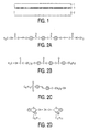
- Fig. 1 is a diagrammatic cross-section of a color filter layer according to the invention. It comprises a layer 1 of a cholesterically ordered material in which the axis of the molecular helix of the cholesteric material extends transversely to the layer.
- the cholesterically ordered material comprises a polymer network and two dyes.
- the cholesterically ordered layer is provided on a substrate 2 of, for example, glass or metal, which is provided with an orientation layer 3 of rubbed polyimide. If desired, the substrate may alternatively consist of a flexible material, for example a synthetic material.
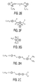
- the color filter layer shown in Fig. 1 was manufactured as follows. The method started from a mixture of two reactive monomers consisting of 50% by weight of the chiral monoacrylate A and 50% by weight of the achiral diacrylate B. Added to this mixture were: 0.7% by weight of an UV-absorbing dye C (Abs max at 334 nm), 0.25% by weight of dye D (Abs max at 485 nm) and 0.25% by weight of of dye E (Abs max at 682 nm). Furthermore, 0.6% by weight of the photoinitiator Irgacure 651 (Ciba Geigy) and 40 ppm of the stabilizer p-methoxyphenol were added to the mixture. The chemical structure formulas of said compounds are shown in Fig. 2.
- a quantity of the mixture thus manufactured was introduced between two substantially parallel glass substrates spaced apart by approximately 15 ⁇ m.
- the facing surfaces of the substrates were provided with an orientation layer of rubbed polyimide.
- a relatively broadband color filter layer having a three-dimensional polymer network was obtained.
- one of the two substrates was removed.
- Fig. 3 shows diagrammatically a combination of the absorption spectrum and the reflection spectrum of the color filter layer described hereinbefore.
- the reference numerals 1 and 2 denote the absorption spectra of the dyes D and E. They leave open a relatively narrow transmission range between approximately 545 nm and 588 nm.
- the reference numeral 3 denotes the reflection spectrum of the cholesterically ordered material of the color filter layer for unpolarized light. This was measured perpendicularly to the layer in the absence of the dyes D and E.
- the reflection spectrum has a bandwidth of approximately 80 nm and ranges from 543 nm to 625 nm. Due to the presence of said dyes, the color filter layer actually reflects only light in the range between 545 nm and 588 nm. The visible light outside this range is absorbed by the dyes D and E.
- the reference numeral 4 denotes the reflection spectrum of the cholesterically ordered material of the color filter layer for unpolarized light. This was measured at an angle of 45° under the normal of the layer and in the absence of the dyes D and E. Under these circumstances, the entire reflection spectrum has moved to a lower wavelength and now ranges between approximately 525 nm and 608 nm. The bandwidth remains approximately equal (80 nm). Due to the presence of said dyes, the color filter layer now actually also reflects only light in the range between 545 nm and 588 nm. The visible light outside this range is absorbed by the dyes D and E.
- Fig. 4 is a diagrammatic cross-section of a liquid crystal color display device of the reflective type according to the invention. It comprises a transparent substrate 11 of, for example glass, a surface of which is provided with a black absorbing layer 12, for example of a black lacquer. The other surface is provided with a thin orientation layer (not shown) on which a pattern of red (R), green (G) and blue (B) color filters is provided.
- each filter consists of a layer polymerized to a three-dimensional network having a thickness of approximately 5 ⁇ m of cholesterically ordered liquid crystalline material having the wavelength associated with the desired color, and at least one dye.
- a 1/4 ⁇ retardation layer (not shown) of approximately 1 ⁇ m thickness is provided on the color filter layer thus formed, dependent on the birefringence of the liquid crystalline material.
- This retardation layer may be made of a uniaxially nematic liquid crystalline material or of a glass-forming liquid crystalline material.
- An orientation layer of rubbed polyimide is used for aligning this layer which can be provided by means of spin-coating.
- An electrode layer 13 of transparent material is provided on the retardation layer. Good results are achieved with ITO-like materials which can be provided in patterns by means of sputtering.
- An orientation layer 14 for orienting the layer 15 of liquid crystalline material to be switched is present on this electrode layer. This orientation layer is present between the above-mentioned substrate 11 and a second transparent substrate 17 which may also be made of glass. This substrate is also provided with an electrode layer 18 and an orientation layer 19.
- the rows of electrodes of the electrode layers 13 and 18 jointly constitute an electrode array with which small areas (pixels) of a layer 15 can be driven via an electric field.
- the size of these areas approximately corresponds to the size of the smallest dimensions of the patterned color filter layer.
- the liquid crystal color display device shown in Fig. 4 also comprises a polarizer layer 20. This layer is provided on the surface of the substrate 17 remote from the substrate 11.
- the color filter of the reflective display device according to the invention was manufactured as follows. A thin layer comprising the above-mentioned mixture of reactive acrylates with dyes was provided on the orientation layer on the substrate 11. The ratio between the two acrylates was chosen to be such that the desired reflection wavelength range was obtained. This is the range between approximately 610 nm and 670 nm for the red pixels, the range between approximately 490 and 540 nm for the green pixels and the range between approximately 435 and 475 nm for the blue pixels.
- a first layer was provided for, for example the red pixels
- the layer was oriented by means of a matrix which was also provided with an orientation layer.
- pattern exposure took place.
- a second layer for, for example the green pixels was provided. It was provided with a matrix in the same manner and subjected to a pattern exposure. This method was finally repeated for providing the blue pixels.
- a thin planarization layer may be provided, if desired, before providing the retardation layer. Subsequently, an electrode layer and an orientation layer were consecutively provided on the retardation layer.
- a display device was manufactured by means of the substrate thus obtained.
- a second substrate was provided with a polarizer, an electrode layer and an orientation layer as described with reference to Fig. 4 and a cell was formed which was filled with a liquid crystalline material.
- the extent of color shift was examined by viewing the different pixel colors of the cell, both perpendicularly to the cell and at an angle of 45°.
Landscapes
- Physics & Mathematics (AREA)
- Nonlinear Science (AREA)
- Chemical & Material Sciences (AREA)
- Crystallography & Structural Chemistry (AREA)
- General Physics & Mathematics (AREA)
- Optics & Photonics (AREA)
- Mathematical Physics (AREA)
- Engineering & Computer Science (AREA)
- Manufacturing & Machinery (AREA)
- Liquid Crystal (AREA)
- Optical Filters (AREA)
Priority Applications (1)
| Application Number | Priority Date | Filing Date | Title |
|---|---|---|---|
| EP99960991A EP1051657B1 (en) | 1998-12-01 | 1999-11-18 | Color filter layer of cholesterically ordered material, and reflective lcd provided with such a color filter layer |
Applications Claiming Priority (4)
| Application Number | Priority Date | Filing Date | Title |
|---|---|---|---|
| EP98204054 | 1998-12-01 | ||
| EP98204054 | 1998-12-01 | ||
| PCT/EP1999/008944 WO2000033129A1 (en) | 1998-12-01 | 1999-11-18 | Color filter layer of cholesterically ordered material, and reflective lcd provided with such a color filter layer |
| EP99960991A EP1051657B1 (en) | 1998-12-01 | 1999-11-18 | Color filter layer of cholesterically ordered material, and reflective lcd provided with such a color filter layer |
Publications (2)
| Publication Number | Publication Date |
|---|---|
| EP1051657A1 EP1051657A1 (en) | 2000-11-15 |
| EP1051657B1 true EP1051657B1 (en) | 2006-09-27 |
Family
ID=8234416
Family Applications (1)
| Application Number | Title | Priority Date | Filing Date |
|---|---|---|---|
| EP99960991A Expired - Lifetime EP1051657B1 (en) | 1998-12-01 | 1999-11-18 | Color filter layer of cholesterically ordered material, and reflective lcd provided with such a color filter layer |
Country Status (6)
| Country | Link |
|---|---|
| US (1) | US6177216B1 (enExample) |
| EP (1) | EP1051657B1 (enExample) |
| JP (1) | JP2002531874A (enExample) |
| KR (1) | KR100624045B1 (enExample) |
| DE (1) | DE69933364T2 (enExample) |
| WO (1) | WO2000033129A1 (enExample) |
Cited By (1)
| Publication number | Priority date | Publication date | Assignee | Title |
|---|---|---|---|---|
| CN104910701A (zh) * | 2015-06-29 | 2015-09-16 | 京东方科技集团股份有限公司 | 一种组合物、紫外吸收带、液晶显示面板及其制造方法 |
Families Citing this family (32)
| Publication number | Priority date | Publication date | Assignee | Title |
|---|---|---|---|---|
| US6693689B1 (en) * | 1999-03-31 | 2004-02-17 | Lg Philips Lcd Co., Ltd. | Reflective liquid crystal display device |
| KR100301854B1 (ko) * | 1999-06-02 | 2001-09-29 | 구본준, 론 위라하디락사 | 투과 및 반사형 겸용 액정표시장치 |
| JP3296333B2 (ja) * | 1999-06-15 | 2002-06-24 | 日本電気株式会社 | 液晶表示方法、液晶パネルおよび液晶表示装置 |
| CN1166979C (zh) * | 1999-06-22 | 2004-09-15 | 日石三菱株式会社 | 反射型液晶显示器件 |
| KR100308855B1 (ko) * | 1999-07-21 | 2001-11-01 | 구본준, 론 위라하디락사 | 콜레스테릭 액정 칼라필터 기판 |
| KR100691320B1 (ko) * | 2000-02-10 | 2007-03-12 | 엘지.필립스 엘시디 주식회사 | 콜레스테릭 액정 컬러필터를 갖는 반사형 액정표시장치 |
| US7408696B2 (en) | 2000-03-03 | 2008-08-05 | Sipix Imaging, Inc. | Three-dimensional electrophoretic displays |
| JP4651791B2 (ja) * | 2000-08-29 | 2011-03-16 | Nec液晶テクノロジー株式会社 | 反射型液晶表示装置、その製造方法、及びその駆動方法 |
| CN1459035A (zh) | 2001-03-16 | 2003-11-26 | 皇家菲利浦电子有限公司 | 胆甾醇型彩色滤光片 |
| US7015993B2 (en) | 2001-03-16 | 2006-03-21 | Koninklijke Philips Electronics N.V. | Reflective color filter and display device including the same |
| KR100790353B1 (ko) * | 2001-05-11 | 2008-01-02 | 엘지.필립스 엘시디 주식회사 | 반사형 액정 표시 장치 및 그의 제조 방법 |
| JP2002357717A (ja) * | 2001-06-01 | 2002-12-13 | Dainippon Printing Co Ltd | 波長選択素子およびそれを備えた光表示装置 |
| EP1425627A2 (en) * | 2001-09-13 | 2004-06-09 | Sipix Imaging, Inc. | Three-dimensional electrophoretic displays |
| JP2003082352A (ja) | 2001-09-17 | 2003-03-19 | Fuji Photo Film Co Ltd | 液晶組成物、選択反射膜、及びその製造方法 |
| JP3849923B2 (ja) * | 2001-11-06 | 2006-11-22 | 大日本印刷株式会社 | 液晶表示装置 |
| KR100485530B1 (ko) * | 2001-12-19 | 2005-04-27 | 엘지.필립스 엘시디 주식회사 | 액정 표시 장치 및 그 제조 방법 |
| US20040090577A1 (en) * | 2002-03-20 | 2004-05-13 | Kazutaka Hara | Bandpass filter for a liquid crystal display, liquid crystal display using the bandpass filter and method of manufacturing the bandpass filter |
| WO2003103068A2 (en) | 2002-05-31 | 2003-12-11 | Koninklijke Philips Electronics N.V. | Electroluminescent device |
| DE10325610A1 (de) * | 2003-06-05 | 2004-12-30 | Consortium für elektrochemische Industrie GmbH | Polymerfilm mit helikaler Molekularstruktur |
| JP4660721B2 (ja) * | 2004-11-12 | 2011-03-30 | 独立行政法人理化学研究所 | アゾベンゼン誘導体化合物、粒子およびその製造方法 |
| KR100729855B1 (ko) * | 2005-08-19 | 2007-06-18 | 엘지전자 주식회사 | 유기 전계 발광 소자 |
| JP2007074635A (ja) * | 2005-09-09 | 2007-03-22 | Matsushita Electric Ind Co Ltd | 画像入力装置および固体撮像素子 |
| JP2007326846A (ja) * | 2006-05-11 | 2007-12-20 | Institute Of Physical & Chemical Research | アゾベンゼン誘導体、蛍光性粒子およびその製造方法 |
| US20090316060A1 (en) | 2008-06-18 | 2009-12-24 | 3M Innovative Properties Company | Conducting film or electrode with improved optical and electrical performance |
| US9581870B2 (en) * | 2009-08-13 | 2017-02-28 | 3M Innovative Properties Company | Conducting film or electrode with improved optical and electrical performance for display and lighting devices and solar cells |
| KR101636052B1 (ko) * | 2010-04-23 | 2016-07-04 | 삼성전자주식회사 | 컬러 필터 및 이를 채용한 디스플레이 장치 |
| KR101720724B1 (ko) * | 2010-12-09 | 2017-04-03 | 삼성디스플레이 주식회사 | 액정 표시 장치 및 그 제조 방법 |
| JP6075604B2 (ja) * | 2012-09-04 | 2017-02-08 | Dic株式会社 | 光学部材及びこれを用いた有機エレクトロルミネッセンス素子 |
| DE112014002328T5 (de) * | 2013-05-08 | 2016-01-21 | Fujifilm Corporation | Zirkulär polarisierter Licht-Separationsfilm, Verfahren zur Erzeugung eines zirkulär polarisierten Licht-Separationsfilmes, Infrarot-Sensor und Abtastsystem und Abtastverfahren unter Verwendung von Licht |
| KR102147672B1 (ko) * | 2014-05-26 | 2020-08-26 | 스미또모 가가꾸 가부시키가이샤 | 조성물 |
| CN104808397B (zh) * | 2015-05-22 | 2018-04-03 | 京东方科技集团股份有限公司 | 一种液晶显示面板及其制作方法、显示装置 |
| CN107561613A (zh) * | 2016-06-30 | 2018-01-09 | 旭硝子株式会社 | 紫外线透射滤波器 |
Family Cites Families (5)
| Publication number | Priority date | Publication date | Assignee | Title |
|---|---|---|---|---|
| JP3268858B2 (ja) * | 1992-11-30 | 2002-03-25 | 三洋電機株式会社 | 液晶表示装置 |
| TW289095B (enExample) * | 1993-01-11 | 1996-10-21 | ||
| DE4328785A1 (de) * | 1993-08-26 | 1995-03-02 | Consortium Elektrochem Ind | Optische Elemente mit abbildender farb- und polarisationsselektiver Reflexion enthaltend cholesterische Flüssigkristalle sowie Herstellung und Verwendung dieser Elemente |
| JPH07239471A (ja) * | 1994-02-28 | 1995-09-12 | Hitachi Ltd | 反射型液晶表示装置 |
| DE4419239A1 (de) * | 1994-06-01 | 1995-12-07 | Consortium Elektrochem Ind | Optische Elemente mit farb- und polarisationsselektiver Reflexion enthaltend LC-Pigmente sowie Herstellung dieser Elemente |
-
1999
- 1999-11-18 WO PCT/EP1999/008944 patent/WO2000033129A1/en not_active Ceased
- 1999-11-18 JP JP2000585709A patent/JP2002531874A/ja not_active Withdrawn
- 1999-11-18 DE DE69933364T patent/DE69933364T2/de not_active Expired - Fee Related
- 1999-11-18 EP EP99960991A patent/EP1051657B1/en not_active Expired - Lifetime
- 1999-11-18 KR KR1020007008314A patent/KR100624045B1/ko not_active Expired - Fee Related
- 1999-11-29 US US09/450,233 patent/US6177216B1/en not_active Expired - Fee Related
Cited By (1)
| Publication number | Priority date | Publication date | Assignee | Title |
|---|---|---|---|---|
| CN104910701A (zh) * | 2015-06-29 | 2015-09-16 | 京东方科技集团股份有限公司 | 一种组合物、紫外吸收带、液晶显示面板及其制造方法 |
Also Published As
| Publication number | Publication date |
|---|---|
| DE69933364D1 (de) | 2006-11-09 |
| KR20010034485A (ko) | 2001-04-25 |
| EP1051657A1 (en) | 2000-11-15 |
| JP2002531874A (ja) | 2002-09-24 |
| KR100624045B1 (ko) | 2006-09-18 |
| US6177216B1 (en) | 2001-01-23 |
| DE69933364T2 (de) | 2007-08-23 |
| WO2000033129A1 (en) | 2000-06-08 |
Similar Documents
| Publication | Publication Date | Title |
|---|---|---|
| EP1051657B1 (en) | Color filter layer of cholesterically ordered material, and reflective lcd provided with such a color filter layer | |
| EP0952478B1 (en) | Liquid crystal display with internal polarizer and method of making same | |
| US7812919B2 (en) | Cholesteric liquid crystal light modulators | |
| US5305126A (en) | Polymer-dispersed liquid crystal material with in-situ polymerized liquid crystal polymer grains dispersed in a layer of liquid crystal material sealed between substrates and field electrodes | |
| US6717644B2 (en) | Optical component and method of manufacture | |
| KR100376193B1 (ko) | 광학 소자 및 이의 제조방법 | |
| US7232594B2 (en) | Polarizer and liquid crystal display element | |
| US6141071A (en) | Switchable achromatic polarization rotator | |
| JP3304054B2 (ja) | スイッチング可能な液晶装置およびその製造方法 | |
| US6078370A (en) | Method of constructing an array of pixels for use in a multi-pixel liquid crystal display | |
| EP1295167B1 (en) | Liquid crystal display including o-type & e-type polarisers | |
| US20060046163A1 (en) | Color filter and liquid crystal display device comprising such filter | |
| GB2324881A (en) | Patterned optical elements | |
| JP2000137226A (ja) | 液晶表示装置 | |
| US20050105026A1 (en) | Combination of cholesteric layer and alignment layer | |
| JPH08313899A (ja) | 反射型液晶表示装置 | |
| JP3524245B2 (ja) | 液晶表示素子 | |
| WO2025093336A1 (en) | Optical structure, anti-reflective device and method for manufacturing such optical structure | |
| Cho et al. | Bistable reflective cholesteric liquid crystal display with pixelated colors |
Legal Events
| Date | Code | Title | Description |
|---|---|---|---|
| PUAI | Public reference made under article 153(3) epc to a published international application that has entered the european phase |
Free format text: ORIGINAL CODE: 0009012 |
|
| AK | Designated contracting states |
Kind code of ref document: A1 Designated state(s): AT BE CH CY DE DK ES FI FR GB GR IE IT LI LU MC NL PT SE |
|
| AX | Request for extension of the european patent |
Free format text: AL;LT;LV;MK;RO;SI |
|
| 17P | Request for examination filed |
Effective date: 20001208 |
|
| RBV | Designated contracting states (corrected) |
Designated state(s): DE FR GB |
|
| GRAP | Despatch of communication of intention to grant a patent |
Free format text: ORIGINAL CODE: EPIDOSNIGR1 |
|
| GRAS | Grant fee paid |
Free format text: ORIGINAL CODE: EPIDOSNIGR3 |
|
| GRAA | (expected) grant |
Free format text: ORIGINAL CODE: 0009210 |
|
| AK | Designated contracting states |
Kind code of ref document: B1 Designated state(s): DE FR GB |
|
| REG | Reference to a national code |
Ref country code: GB Ref legal event code: FG4D |
|
| REF | Corresponds to: |
Ref document number: 69933364 Country of ref document: DE Date of ref document: 20061109 Kind code of ref document: P |
|
| PGFP | Annual fee paid to national office [announced via postgrant information from national office to epo] |
Ref country code: GB Payment date: 20061127 Year of fee payment: 8 |
|
| PGFP | Annual fee paid to national office [announced via postgrant information from national office to epo] |
Ref country code: FR Payment date: 20061129 Year of fee payment: 8 |
|
| PGFP | Annual fee paid to national office [announced via postgrant information from national office to epo] |
Ref country code: DE Payment date: 20070110 Year of fee payment: 8 |
|
| ET | Fr: translation filed | ||
| PLBE | No opposition filed within time limit |
Free format text: ORIGINAL CODE: 0009261 |
|
| STAA | Information on the status of an ep patent application or granted ep patent |
Free format text: STATUS: NO OPPOSITION FILED WITHIN TIME LIMIT |
|
| 26N | No opposition filed |
Effective date: 20070628 |
|
| GBPC | Gb: european patent ceased through non-payment of renewal fee |
Effective date: 20071118 |
|
| PG25 | Lapsed in a contracting state [announced via postgrant information from national office to epo] |
Ref country code: DE Free format text: LAPSE BECAUSE OF NON-PAYMENT OF DUE FEES Effective date: 20080603 |
|
| REG | Reference to a national code |
Ref country code: FR Ref legal event code: ST Effective date: 20080930 |
|
| PG25 | Lapsed in a contracting state [announced via postgrant information from national office to epo] |
Ref country code: GB Free format text: LAPSE BECAUSE OF NON-PAYMENT OF DUE FEES Effective date: 20071118 |
|
| PG25 | Lapsed in a contracting state [announced via postgrant information from national office to epo] |
Ref country code: FR Free format text: LAPSE BECAUSE OF NON-PAYMENT OF DUE FEES Effective date: 20071130 |