EP1046726B1 - Sputtering method for the formation of carbon films - Google Patents
Sputtering method for the formation of carbon films Download PDFInfo
- Publication number
- EP1046726B1 EP1046726B1 EP00303307A EP00303307A EP1046726B1 EP 1046726 B1 EP1046726 B1 EP 1046726B1 EP 00303307 A EP00303307 A EP 00303307A EP 00303307 A EP00303307 A EP 00303307A EP 1046726 B1 EP1046726 B1 EP 1046726B1
- Authority
- EP
- European Patent Office
- Prior art keywords
- carbon
- film
- sputtering
- voltage
- target
- Prior art date
- Legal status (The legal status is an assumption and is not a legal conclusion. Google has not performed a legal analysis and makes no representation as to the accuracy of the status listed.)
- Expired - Lifetime
Links
- 229910052799 carbon Inorganic materials 0.000 title claims description 157
- OKTJSMMVPCPJKN-UHFFFAOYSA-N Carbon Chemical compound [C] OKTJSMMVPCPJKN-UHFFFAOYSA-N 0.000 title claims description 148
- 238000004544 sputter deposition Methods 0.000 title claims description 73
- 230000015572 biosynthetic process Effects 0.000 title description 9
- 238000000034 method Methods 0.000 claims description 85
- 239000000758 substrate Substances 0.000 claims description 38
- 238000000151 deposition Methods 0.000 claims description 36
- 230000008569 process Effects 0.000 claims description 30
- 230000005291 magnetic effect Effects 0.000 claims description 24
- UFHFLCQGNIYNRP-UHFFFAOYSA-N Hydrogen Chemical compound [H][H] UFHFLCQGNIYNRP-UHFFFAOYSA-N 0.000 claims description 15
- 239000007789 gas Substances 0.000 claims description 15
- 239000001257 hydrogen Substances 0.000 claims description 15
- 229910052739 hydrogen Inorganic materials 0.000 claims description 15
- UFWIBTONFRDIAS-UHFFFAOYSA-N Naphthalene Chemical compound C1=CC=CC2=CC=CC=C21 UFWIBTONFRDIAS-UHFFFAOYSA-N 0.000 claims description 6
- HSFWRNGVRCDJHI-UHFFFAOYSA-N alpha-acetylene Natural products C#C HSFWRNGVRCDJHI-UHFFFAOYSA-N 0.000 claims description 4
- 125000002534 ethynyl group Chemical group [H]C#C* 0.000 claims description 4
- VGGSQFUCUMXWEO-UHFFFAOYSA-N Ethene Chemical compound C=C VGGSQFUCUMXWEO-UHFFFAOYSA-N 0.000 claims description 3
- 239000005977 Ethylene Substances 0.000 claims description 3
- 239000001273 butane Substances 0.000 claims description 3
- IJDNQMDRQITEOD-UHFFFAOYSA-N n-butane Chemical compound CCCC IJDNQMDRQITEOD-UHFFFAOYSA-N 0.000 claims description 3
- OFBQJSOFQDEBGM-UHFFFAOYSA-N n-pentane Natural products CCCCC OFBQJSOFQDEBGM-UHFFFAOYSA-N 0.000 claims description 3
- 239000011241 protective layer Substances 0.000 claims description 2
- 238000005471 reflection electron energy loss spectroscopy Methods 0.000 claims description 2
- 150000002431 hydrogen Chemical class 0.000 claims 1
- 239000010408 film Substances 0.000 description 200
- 230000008021 deposition Effects 0.000 description 31
- 238000000623 plasma-assisted chemical vapour deposition Methods 0.000 description 26
- 238000007737 ion beam deposition Methods 0.000 description 23
- 239000010410 layer Substances 0.000 description 21
- 238000010884 ion-beam technique Methods 0.000 description 18
- 230000007797 corrosion Effects 0.000 description 17
- 238000005260 corrosion Methods 0.000 description 17
- 229910003481 amorphous carbon Inorganic materials 0.000 description 15
- -1 carbon ions Chemical class 0.000 description 11
- 238000004519 manufacturing process Methods 0.000 description 11
- 229910017052 cobalt Inorganic materials 0.000 description 9
- 239000010941 cobalt Substances 0.000 description 9
- 230000000694 effects Effects 0.000 description 9
- 230000006870 function Effects 0.000 description 9
- 239000000463 material Substances 0.000 description 9
- GUTLYIVDDKVIGB-UHFFFAOYSA-N cobalt atom Chemical compound [Co] GUTLYIVDDKVIGB-UHFFFAOYSA-N 0.000 description 8
- 238000012360 testing method Methods 0.000 description 8
- 230000008901 benefit Effects 0.000 description 7
- 230000007547 defect Effects 0.000 description 7
- 239000004215 Carbon black (E152) Substances 0.000 description 6
- 239000011651 chromium Substances 0.000 description 6
- 229930195733 hydrocarbon Natural products 0.000 description 6
- 150000002430 hydrocarbons Chemical class 0.000 description 6
- 238000005259 measurement Methods 0.000 description 6
- 239000002245 particle Substances 0.000 description 6
- 238000001069 Raman spectroscopy Methods 0.000 description 5
- 229910052804 chromium Inorganic materials 0.000 description 5
- 238000013461 design Methods 0.000 description 5
- 229910002804 graphite Inorganic materials 0.000 description 5
- 239000010439 graphite Substances 0.000 description 5
- 239000010409 thin film Substances 0.000 description 5
- IJGRMHOSHXDMSA-UHFFFAOYSA-N Atomic nitrogen Chemical compound N#N IJGRMHOSHXDMSA-UHFFFAOYSA-N 0.000 description 4
- VYZAMTAEIAYCRO-UHFFFAOYSA-N Chromium Chemical compound [Cr] VYZAMTAEIAYCRO-UHFFFAOYSA-N 0.000 description 4
- 229910000599 Cr alloy Inorganic materials 0.000 description 4
- 238000004458 analytical method Methods 0.000 description 4
- XKRFYHLGVUSROY-UHFFFAOYSA-N argon Substances [Ar] XKRFYHLGVUSROY-UHFFFAOYSA-N 0.000 description 4
- 150000002500 ions Chemical class 0.000 description 4
- 230000004044 response Effects 0.000 description 4
- 238000001228 spectrum Methods 0.000 description 4
- 239000000654 additive Substances 0.000 description 3
- XAGFODPZIPBFFR-UHFFFAOYSA-N aluminium Chemical compound [Al] XAGFODPZIPBFFR-UHFFFAOYSA-N 0.000 description 3
- 229910052782 aluminium Inorganic materials 0.000 description 3
- 229910052786 argon Inorganic materials 0.000 description 3
- 230000009286 beneficial effect Effects 0.000 description 3
- 238000010586 diagram Methods 0.000 description 3
- 229910003460 diamond Inorganic materials 0.000 description 3
- 239000010432 diamond Substances 0.000 description 3
- 238000000605 extraction Methods 0.000 description 3
- 239000011521 glass Substances 0.000 description 3
- 230000001681 protective effect Effects 0.000 description 3
- 229910000943 NiAl Inorganic materials 0.000 description 2
- 238000001237 Raman spectrum Methods 0.000 description 2
- NPXOKRUENSOPAO-UHFFFAOYSA-N Raney nickel Chemical compound [Al].[Ni] NPXOKRUENSOPAO-UHFFFAOYSA-N 0.000 description 2
- 125000004429 atom Chemical group 0.000 description 2
- 230000008859 change Effects 0.000 description 2
- 239000000788 chromium alloy Substances 0.000 description 2
- 230000003749 cleanliness Effects 0.000 description 2
- 239000002241 glass-ceramic Substances 0.000 description 2
- 230000006872 improvement Effects 0.000 description 2
- 238000010348 incorporation Methods 0.000 description 2
- 239000010687 lubricating oil Substances 0.000 description 2
- 230000007246 mechanism Effects 0.000 description 2
- 239000000203 mixture Substances 0.000 description 2
- 238000012986 modification Methods 0.000 description 2
- 230000004048 modification Effects 0.000 description 2
- 229910052757 nitrogen Inorganic materials 0.000 description 2
- 230000024121 nodulation Effects 0.000 description 2
- 230000003287 optical effect Effects 0.000 description 2
- BASFCYQUMIYNBI-UHFFFAOYSA-N platinum Chemical compound [Pt] BASFCYQUMIYNBI-UHFFFAOYSA-N 0.000 description 2
- 239000000523 sample Substances 0.000 description 2
- 239000000126 substance Substances 0.000 description 2
- XLYOFNOQVPJJNP-UHFFFAOYSA-N water Substances O XLYOFNOQVPJJNP-UHFFFAOYSA-N 0.000 description 2
- 235000001674 Agaricus brunnescens Nutrition 0.000 description 1
- ZOXJGFHDIHLPTG-UHFFFAOYSA-N Boron Chemical compound [B] ZOXJGFHDIHLPTG-UHFFFAOYSA-N 0.000 description 1
- 229910000531 Co alloy Inorganic materials 0.000 description 1
- 238000010521 absorption reaction Methods 0.000 description 1
- 230000000996 additive effect Effects 0.000 description 1
- 229910045601 alloy Inorganic materials 0.000 description 1
- 239000000956 alloy Substances 0.000 description 1
- 238000013459 approach Methods 0.000 description 1
- 230000006399 behavior Effects 0.000 description 1
- 238000005513 bias potential Methods 0.000 description 1
- 230000005540 biological transmission Effects 0.000 description 1
- 229910052796 boron Inorganic materials 0.000 description 1
- 239000006227 byproduct Substances 0.000 description 1
- 125000004432 carbon atom Chemical group C* 0.000 description 1
- 238000012512 characterization method Methods 0.000 description 1
- 238000005229 chemical vapour deposition Methods 0.000 description 1
- 150000001868 cobalt Chemical class 0.000 description 1
- 229910001429 cobalt ion Inorganic materials 0.000 description 1
- 229910000428 cobalt oxide Inorganic materials 0.000 description 1
- GUBSQCSIIDQXLB-UHFFFAOYSA-N cobalt platinum Chemical compound [Co].[Pt].[Pt].[Pt] GUBSQCSIIDQXLB-UHFFFAOYSA-N 0.000 description 1
- XLJKHNWPARRRJB-UHFFFAOYSA-N cobalt(2+) Chemical compound [Co+2] XLJKHNWPARRRJB-UHFFFAOYSA-N 0.000 description 1
- IVMYJDGYRUAWML-UHFFFAOYSA-N cobalt(ii) oxide Chemical compound [Co]=O IVMYJDGYRUAWML-UHFFFAOYSA-N 0.000 description 1
- 238000010276 construction Methods 0.000 description 1
- 238000000354 decomposition reaction Methods 0.000 description 1
- 230000032798 delamination Effects 0.000 description 1
- 230000001419 dependent effect Effects 0.000 description 1
- 238000001514 detection method Methods 0.000 description 1
- 230000006866 deterioration Effects 0.000 description 1
- 230000001627 detrimental effect Effects 0.000 description 1
- 238000005516 engineering process Methods 0.000 description 1
- 230000007613 environmental effect Effects 0.000 description 1
- 239000006112 glass ceramic composition Substances 0.000 description 1
- 231100001261 hazardous Toxicity 0.000 description 1
- 238000010438 heat treatment Methods 0.000 description 1
- 239000012212 insulator Substances 0.000 description 1
- 238000004255 ion exchange chromatography Methods 0.000 description 1
- 239000000314 lubricant Substances 0.000 description 1
- 229910001004 magnetic alloy Inorganic materials 0.000 description 1
- 238000001755 magnetron sputter deposition Methods 0.000 description 1
- 238000012423 maintenance Methods 0.000 description 1
- 229910052758 niobium Inorganic materials 0.000 description 1
- 239000010955 niobium Substances 0.000 description 1
- GUCVJGMIXFAOAE-UHFFFAOYSA-N niobium atom Chemical compound [Nb] GUCVJGMIXFAOAE-UHFFFAOYSA-N 0.000 description 1
- 229910052697 platinum Inorganic materials 0.000 description 1
- 230000002028 premature Effects 0.000 description 1
- 238000002360 preparation method Methods 0.000 description 1
- 230000009467 reduction Effects 0.000 description 1
- 230000001105 regulatory effect Effects 0.000 description 1
- 238000011160 research Methods 0.000 description 1
- 238000012552 review Methods 0.000 description 1
- 239000004065 semiconductor Substances 0.000 description 1
- 238000004611 spectroscopical analysis Methods 0.000 description 1
- 238000005478 sputtering type Methods 0.000 description 1
- 230000003068 static effect Effects 0.000 description 1
- 238000003860 storage Methods 0.000 description 1
- 229910052715 tantalum Inorganic materials 0.000 description 1
- GUVRBAGPIYLISA-UHFFFAOYSA-N tantalum atom Chemical compound [Ta] GUVRBAGPIYLISA-UHFFFAOYSA-N 0.000 description 1
- 239000013077 target material Substances 0.000 description 1
Images


Classifications
-
- G—PHYSICS
- G11—INFORMATION STORAGE
- G11B—INFORMATION STORAGE BASED ON RELATIVE MOVEMENT BETWEEN RECORD CARRIER AND TRANSDUCER
- G11B5/00—Recording by magnetisation or demagnetisation of a record carrier; Reproducing by magnetic means; Record carriers therefor
- G11B5/84—Processes or apparatus specially adapted for manufacturing record carriers
- G11B5/8408—Processes or apparatus specially adapted for manufacturing record carriers protecting the magnetic layer
-
- C—CHEMISTRY; METALLURGY
- C23—COATING METALLIC MATERIAL; COATING MATERIAL WITH METALLIC MATERIAL; CHEMICAL SURFACE TREATMENT; DIFFUSION TREATMENT OF METALLIC MATERIAL; COATING BY VACUUM EVAPORATION, BY SPUTTERING, BY ION IMPLANTATION OR BY CHEMICAL VAPOUR DEPOSITION, IN GENERAL; INHIBITING CORROSION OF METALLIC MATERIAL OR INCRUSTATION IN GENERAL
- C23C—COATING METALLIC MATERIAL; COATING MATERIAL WITH METALLIC MATERIAL; SURFACE TREATMENT OF METALLIC MATERIAL BY DIFFUSION INTO THE SURFACE, BY CHEMICAL CONVERSION OR SUBSTITUTION; COATING BY VACUUM EVAPORATION, BY SPUTTERING, BY ION IMPLANTATION OR BY CHEMICAL VAPOUR DEPOSITION, IN GENERAL
- C23C14/00—Coating by vacuum evaporation, by sputtering or by ion implantation of the coating forming material
- C23C14/06—Coating by vacuum evaporation, by sputtering or by ion implantation of the coating forming material characterised by the coating material
- C23C14/0605—Carbon
-
- C—CHEMISTRY; METALLURGY
- C23—COATING METALLIC MATERIAL; COATING MATERIAL WITH METALLIC MATERIAL; CHEMICAL SURFACE TREATMENT; DIFFUSION TREATMENT OF METALLIC MATERIAL; COATING BY VACUUM EVAPORATION, BY SPUTTERING, BY ION IMPLANTATION OR BY CHEMICAL VAPOUR DEPOSITION, IN GENERAL; INHIBITING CORROSION OF METALLIC MATERIAL OR INCRUSTATION IN GENERAL
- C23C—COATING METALLIC MATERIAL; COATING MATERIAL WITH METALLIC MATERIAL; SURFACE TREATMENT OF METALLIC MATERIAL BY DIFFUSION INTO THE SURFACE, BY CHEMICAL CONVERSION OR SUBSTITUTION; COATING BY VACUUM EVAPORATION, BY SPUTTERING, BY ION IMPLANTATION OR BY CHEMICAL VAPOUR DEPOSITION, IN GENERAL
- C23C14/00—Coating by vacuum evaporation, by sputtering or by ion implantation of the coating forming material
- C23C14/22—Coating by vacuum evaporation, by sputtering or by ion implantation of the coating forming material characterised by the process of coating
- C23C14/34—Sputtering
-
- G—PHYSICS
- G11—INFORMATION STORAGE
- G11B—INFORMATION STORAGE BASED ON RELATIVE MOVEMENT BETWEEN RECORD CARRIER AND TRANSDUCER
- G11B5/00—Recording by magnetisation or demagnetisation of a record carrier; Reproducing by magnetic means; Record carriers therefor
- G11B5/84—Processes or apparatus specially adapted for manufacturing record carriers
- G11B5/851—Coating a support with a magnetic layer by sputtering
Definitions
- This invention relates to a method of and apparatus for depositing amorphous carbon thin films that protect the magnetic media used in hard disk drives, to the media so formed, and to disk drives incorporating the media.
- Metallic magnetic thin film disks used in memory applications typically comprise a substrate material that is coated with a magnetic alloy film that serves as the recording medium.
- the recording medium used in such disks is a cobalt platinum-based alloy such as CoPtCr, CoPtCrTa, CoPtCrB, CoPtCrTaB or other various combinations of elements which is usually deposited by sputtering.
- the magnetic layer typically has an underlayer beneath it, consisting of Cr or Cr alloys, and also may have additional layers or seedlayers such as NiAl below the Cr layer.
- the substrates used for the deposited film are typically aluminum coated with plated NiP, or amorphous glass or glass ceramic materials.
- Magnetic media is typically protected by a thin carbon overcoat film.
- An example of such a sputtered carbon overcoat is described by F.K King in "Datapoint Thin Film Media", published in IEEE Transaction in Magnetics in July 1981 . It is also known to provide a carbon film containing hydrogen by using hydrogen gas during sputtering as described in U.S. Patent No. 5,045,165 by Yamashita .
- the protective overcoat is an extremely important component of thin film magnetic recording disks. When a disk drive is turned on or off, the recording head that normally flies over the recording surface comes into sliding contact with the media. Over the life of the disk drive, the head comes into many such "contact start-stop" with the media surface and the overcoat must protect the media from becoming destroyed in the process.
- the recording head can be pulled away from the disk surface when the drive is not in use or when it is turned off.
- the contact start stop does not take place between the head and the disk surface.
- the designs that allow the head to be pulled to the side of the disk away from the disk surface are generally called ramp-loading mechanisms.
- the recording heads still fly very close to the media surface during operation of the drive, such that occasional contact occurs between the disk surface and the head. Therefore even in the drives using ramp-load mechanisms, the media must still have a protective overcoat.
- the thickness of carbon overcoat film has been steadily reduced over the years so that recording head can be made to fly closer to the magnetic media. As the active element in the head is placed closer to the magnetic layer, higher recording density can be achieved.
- Today, high performance hard disk drives have recording density in the range of 6 - 8 Gbits per square inch (about 1 Gbits per square centimeter).
- a media for such application has an overcoat thickness that is less than 10 nm thick and the recording heads fly at around 30 nm from the top of the carbon film. In order to increase the recording density even higher, there is a strong desire to reduce the carbon overcoat thickness further to 5 nm or even thinner, and also to reduce the flying height of the recording head below 25 nm.
- the media is expected to meet or exceed the reliability of current media having thicker carbon overcoat and higher flying heights.
- Typical measures of reliability are contact start stop capability and corrosion resistance. It has been very difficult to meet such expectations from a conventionally sputtered carbon overcoat as overcoat thickness is reduced below 10 nm.
- a carbon film deposited by sputtering is amorphous. It has no evidence of crystallinity down to the resolution of the most powerful transmission electron microscopes.
- additives such as hydrogen have been added to the film as described in U.S. Patent No. 5,045,165 .
- nitrogen or a combination of nitrogen and hydrogen is also sometimes used to enhance contact start stop performance.
- the sputtering process typically involves applying DC power onto a graphite target.
- a type of sputtering cathode called DC magnetron cathodes are typically used. Depending upon the size and configuration of the cathode, typical voltages that develop on the target are between 300 to 800 volts negative DC with various current level to achieve the necessary deposition rate.
- the DC power can be applied as a pulse, using power supplies described in US 5,810,982 or available from companies such as Advanced Energy Industries, Inc. based in Fort Collins, Colorado for example.
- the pulse rate can be fixed or adjustable to typically 20 kHz to 50 kHz range.
- an AC power supply can be used, or a combination of AC and DC power supply as described by Yamashita et al. in U.S. Patent No. 5,507,930 .
- the carbon films sputtered by these methods have similar atomic structures. The carbon in these films have between 30 to 50% of their bonds in sp 3 bonding configuration depending upon the method of measurement that is used.
- the typical film stress for these films are around 1 to 2 giga-pascal (GPa) compressive for a film of around 10 nm thickness.
- the amorphous carbon film should be distinguished from actual diamond film which is composed of crystalline diamond and has a high sp 3 bonding fraction. Both sputtering and chemical vapor deposition methods such as plasma-enhanced chemical vapor deposition (PE-CVD) and ion-beam deposition produce largely amorphous carbon films. Hydrogen is almost always present to varying degree from the hydrocarbon gas used in the CVD type process, and in the case of sputtering, from deliberate introduction of hydrogen in the plasma. Amorphous carbon films containing a significant amount of hydrogen are categorized as "hydrogenated amorphous carbon films" and designated as a-C:H films.
- the vast majority of sputtered carbon overcoat typically used in the magnetic media can be categorized as a-C:H type carbon film, due to incorporation of 20 to 40% atomic fraction of hydrogen in the film.
- a designation as an a-C or a-C:H carbon film also implies that the fraction of its bond in the sp 3 or tetrahedral bonding configuration is relatively low, typically from around 10 to 50%. It is known that hydrogen incorporation increases sp 3 content of sputtered carbon films to a maximum of around 50% by current knowledge.
- ta-C or ta-C:H carbon film which stands for tetrahedral amorphous carbon film, indicating a high fraction of bonding in the sp3 state.
- the sp 3 bonding fraction in the film should be at least 70% and preferably in the range of 80% or higher.
- Another term often used for the ta-C carbon is "DLC” or diamond-like carbon.
- DLC-carbon has been widely misused so that it may be best not to use this terminology for the amorphous carbon film.
- ta-C or ta-C:H carbon films have superior mechanical and corrosion properties compared to the a-C:H carbon by virtue of the high sp 3 content. It is known to have higher compressive stress, which leads also to a higher hardness in the film. The density is also known to be higher than a-C or a-C:H film, although the density can vary as function of hydrogen content as well. For magnetic hard disk application, it is thought that ta-C:H carbon offers much better properties in terms of contact start-stop and corrosion resistance especially for films less than 10 nm in thickness. There is considerable desire to reduce the film thickness to around 5 nm currently, and even down to 2 nm in the near future. However, these thinner films must not lose any performance compared to current films. Since it is also believed that conventional sputtering method cannot create ta-C:H type carbon film, recent efforts to produce such carbon have focused on the use of PE-CVD or ion-beam deposition method.
- PE-CVD and ion-beam depositions are fundamentally different methods of deposition compared to sputtering.
- the source of carbon in sputtering is typically a graphite target, while in PE-CVD and in ion-beam deposition, the source is hydrocarbon gasses.
- Both PE-CVD and ion-beam deposition can be categorized as forms of CVD, since both use hydrocarbon gas to create the carbon ions that are used to form the film.
- a more detailed description of the ion-beam method of forming the carbon film is described by Weiler et al. in "Preparation and Properties of Highly Tetrahedral Hydrogenated Amorphous Carbon" published in Physical Review B, January 1996 . In a narrow range of deposition condition and energies of carbon ions, Weiler et al. report on fabricating ta-C:H film by their form of ion-beam deposition.
- ta-C:H carbon The benefits of ta-C:H carbon is described by Weiler et al. in the above mentioned article.
- the sp 3 bonding fraction in ta-C:H carbon is as high as 80%, and the film stress is much higher for a given thickness of the film compared to films with lower sp 3 content. Consequently the density and hardness of the film is highest at the highest sp 3 content.
- the process must be tuned fairly precisely, to maintain the energy per carbon atom ion near 100 ev/atom for their method. Otherwise the sp 3 fraction drops precipitously on either side of the energy value.
- the films produced according to Weiler's prescription for ta-C:H carbon film may have several advantageous properties for hard disk application.
- the film known to contain high sp 3 fraction made by ion-beam and PE-CVD method continues to exhibit good contact start-stop performance and corrosion resistance, while conventionally sputtered a-C:H films starts to show a deterioration in performance.
- PE-CVD and ion-beam deposition methods have one common drawback, which is that they create a tremendous amount of flaking and particles during deposition compared to sputtering.
- the hard disk media must be maintained extremely clean. Even a presence of small amount of particles that can be trapped between the disk and the head can cause catastrophic head crashes since the head flies very close to the surface.
- This difficulty has prevented more widespread use of PE-CVD and ion-beam deposition in hard disk manufacturing.
- deposition applications that require only intermittent use of the tool such as in semiconductor and recording head manufacturing
- both PE-CVD and ion-beam methods have found more widespread use.
- the manufacturing tool must run continuously for at least 5 days or more in order for it to be economical.
- the in-line sputtering systems as described in U.S. Patent No. 5,045,165 by Yamashita can run continuously for 4 weeks without opening the system for servicing. It has been difficult to obtain even a few days of continuous deposition out of the CVD or ion-beam deposition tools due to particle generation during deposition. Such short utilization severely impacts the productivity of the expensive deposition tools, and increases the cost of manufacturing.
- the cathodes used for PE-CVD and ion-beam deposition are also expensive compared to comparable sputtering cathodes.
- substrate bias is required in order to obtain the ta-C:H type carbon films. It is more advantageous to have a process which does not require substrate bias since some substrates that are used for hard disk application are insulators, such as glass and glass ceramics. It is necessary to have conductive substrates in order to apply substrate bias to the disk.
- substrates that are used for hard disk application are insulators, such as glass and glass ceramics.
- conductive substrates in order to apply substrate bias to the disk.
- cathode designs have problems that impact their usefulness in continuous deposition tools. In some designs, a hot filament is needed in front of the cathode as source of electrons to energize the plasma.
- the filament can burn out and can be coated with the film of the material to be coated and cause significant reduction in the amount of time that the cathode can be operated.
- the potential that is needed to extract the beam of carbon ions is applied through a thin grid placed in front of the gun. These grids wear out due to bombardment by the ions, or else are coated by the film to be deposited, and therefore must be periodically replaced. The grid also contributes significantly to particle generation as it is rapidly coated during the deposition and begins to flake.
- Manufacturing of hard disk media is typically done in two different type of machines.
- the first is called “in-line” deposition tool, and it is described in U.S. Patent No. 5,045,165 by Yamashita.
- the disks are loaded on large pallets which pass by series of cathodes which deposit the films successively on a disk.
- the disk can be deposited one disk at a time using circular targets or cathodes using a machine tool generally called a "static" deposition tool.
- Such machines are manufactured by Intevac Inc. of Santa Clara, California, Balzers Process Systems, Inc. of Alzenau, Germany and Anelva Corporation of Fuchu-shi, Japan.
- the target can be used up, and the system must be opened to replace it.
- the protective shields that direct the sputtered species to the substrate become coated, and they will eventually start to flake.
- the shields must be periodically replaced and cleaned. Excessive flaking from the shields contributes to increased defects on the disk surface.
- a third factor that is specific to carbon sputtering is that the carbon target has finite run times due to formation of defects on the target surface, which are generally called “nodules,” “warts” or “mushrooms” which degrade the performance of the cathode. Formation of these defects on the target surface contributes to an increased rate of arcing on the target. Arcs cause defects and particles to be deposited on to the disk surface. An increasing rate of these defects can cause premature shut-down of the system. During a shut down, the sputtering system is vented to air and the targets are cleaned or replaced. The time needed to do the maintenance and target changes contributes to a loss of utilization and adds cost to manufacturing. Typically the sputter line is the most expensive capital equipment needed in making the disks, therefore a loss in utilization impacts seriously the overall cost of manufacturing.
- a method described by Yamashita et al. in U.S. Patent No. 5,507,930 teaches one method of reducing nodules on the carbon target surface by use of AC power superimposed on DC which also reduces arcing. Even with such methods however, the carbon target is still susceptible to nodule formation and excessive arcing. Therefore conventional sputtering is still far from being ideal, but it is still more suitable for manufacturing than PE-CVD and ion-beam deposition methods.
- An additional method to reduce nodule formation has been to use a pulsed DC power supply which provides a square wave type positive voltage pulse at a frequency of 20 kHz for a duration (pulse width) of several micro-seconds ( ⁇ -seconds).
- US 5,858,477 discloses forming a film of diamond-like carbon as a protective layer for magnetic recording media.
- the new method can be actually cleaner in terms of particle generation and the target surface can remain very clean during deposition, leading to improved process yields and increased cleanliness of the disk after sputter, compared to conventional sputtering process.
- This can eliminate the necessity of using more complex and expensive PE-CVD or ion-beam disposition method to create the same ta-C or ta-C:H carbon film.
- the first sub-portion value may be 25% or more greater in magnitude than the second value and may be greater in magnitude than the second value and may be greater than approximately 900 volts in magnitude.
- a special type of pulsed DC power supply may be used.
- the special pulsed power supply is capable of providing high voltage spikes or deviations, and hence provide a very high energy pulse to the plasma. Power supplies with such characteristics are manufactured by ENI Inc. of Rochester New York and by Advanced Energy, Inc. of Fort Collins, Colorado. When these special types of power supplies are used in conjunction with sputtering of carbon target under operating conditions and process conditions such as those described herein, the properties of the sputtered carbon films change from conventional a-C:H type with low sp 3 bond fraction to ta-C:H type carbon with high sp 3 bond fraction.
- the pulsed DC power supply can provide adjustable pulse frequency typically 50 kHz to around 200 kHz.
- the range of available frequencies can be used to produce the ta-C:H type carbon film as long as certain pulse characteristics described herein are met.
- the pulse rate and duty cycle of the pulse can be adjusted to obtain a unique voltage and current profile that has not previously been possible with conventional power supplies.
- a particular set of pulse characteristics that creates a ta-C:H type carbon film is described as follows: First the power supply delivers a positive potential to the target, by as much as, e.g. 300 volts positive. In this condition, the argon ions used for deposition are actually repelled away from the target so that no sputtering takes place. Little current flows to the target in the positive swing in voltage and the power supply act as voltage source. Then, the power supply switches and applies a negative potential to the target. The power supply under this condition acts essentially as a current supply which applies whatever voltage necessary to obtain a preset current level. The net effect for the carbon target is that large voltage is imparted to the target momentarily to overcome the positive voltage that had just been applied.
- the negative voltage can be two or three times higher than the steady state negative voltage.
- the large negative swing in the applied potential to the target momentarily causes a high deposition rate and carbon atoms can have much higher energy than in normal sputtering.
- the high rate is not maintained continuously since the voltage spike is only momentary.
- the pulse duty cycle is adjusted so that average deposition rate differs little from continuous DC sputtering mode.
- the substrate can also be biased in order to enhance the ta-C:H characteristics of the carbon film. Although this can only be done with conductive substrates, the effect is pronounced and useful. Nominally che substrate is biased negative to the ground, so that there is potential of additional bombardment of the substrate by the argon ion used to sputter the target or to accelerate the carbon ions that may have formed during sputtering at high target bias potential. When substrate bias is applied, the positive ions will be accelerated toward the substrate during deposition. With nominal substrate bias of only, for example, approximately 50 volts negative, the film property can be adjusted to a higher fraction of sp 3 bonding.
- the substrate temperature is also an additional variable that affects the sp 3 content of the film under this new sputtering method.
- the sp 3 content can be adjusted up or down. Temperatures in the range of around 80 to 150°C are within the preferred operating region of this process. For example, adjustment of substrate temperature during the carbon deposition by only 10 to 20°C can be used to adjust the sp 3 content and the stress of the film by a significant amount. Again, this adjustability of sp 3 content and stress by temperature is not available or seen in conventional sputtering methods. Only in this new pulse sputtering method, is a pronounced effect observed.
- sp 3 content and film stress is an important parameter since there are some adjustments that may be of advantage in tuning the properties of the overcoat around specific drive environment and the type of heads used. Although it may appear to be advantageous to keep increasing sp 3 content, there comes with it a higher film stress. Too high a film stress can cause delamination and other mechanical problems, therefore there is a trade-off between having the good properties of the high sp 3 content and the detrimental effect of too high a stress.
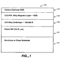
- FIG. 1 is a schematic diagram of a typical hard disk media 100 made according to the current invention.
- the substrate 101 is typically a 95mm, 84mm or 65mm diameter disk made of NiP plated aluminum or amorphous glass or glass ceramic.
- the substrate is polished to a mirror like smoothness upon which various layers are sputtered successively above it.
- the first layer is typically chromium or a chromium alloy layer 102, followed by a magnetic layer 103 consisting of cobalt, platinum and a combination of various additives such as chromium, tantalum, niobium, boron and other additive elements.
- the carbon layer 104 is the final vacuum deposited layer and it is typically sputtered.
- the typical thickness of the chromium or chromium alloy layer 102 is between 5 to 30 nm, the magnetic layer 103 thickness is between 20 to 40 nm, and the carbon layer 104 thickness is typically 10 nm or less. It is usual to also apply a thin 1 to 2 nm thick liquid lubricant on top of the carbon film (not shown). The lubricant is applied after the film deposition. Other variants of the above structure include additional seed layer(s) beneath the chromium, such as NiAl.
- the magnetic layer 103 can be two or more different layers and the carbon film 104 can be composed of two different carbon films for example. The present invention is focused on formation of carbon films for use in media such as that illustrated in Figure 1 .
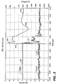
- Figure 2 shows voltage and current waveforms of the output of the RPG model pulse power supply made by ENI Inc. of Rochester New York at a frequency of 50 kHz supplied to a graphite carbon target.
- the system used for the data was obtained from a large in-line sputtering system manufactured by Ulvac Inc. of Japan.
- the carbon target size was 23 cm x 62 cm.
- the sputter pressure was approximately 2.5 m Torr, with Ar gas flow of approximately 45 sccm and H 2 gas flow of approximately 20 sccm.
- the Ar and H 2 are combined and then introduced via tubes containing nozzles disposed proximate the target.
- the DC power is pulsed.
- each pulse comprises an "on” time during which sputtering is occurring and an “off” time, during which little or no sputtering is occurring.
- the frequency refers to the number of on/off cycles per second.
- Pulse length refers to the duration of each pulse (i.e., the inverse of frequency), and “pulse width” in the present description refers to the duration of the off cycle.
- zero voltage, or more commonly some positive voltage is applied to the target and little or no current flows through the system.
- the "duty cycle” generally refers to the percentage of time of the "on” portion of the cycle - i.e. in the present case the time during which the voltage is negative and sputtering occurs.
- the present invention comprises use of a pulsed DC power supply that provides a spike or peak negative voltage for a short period of time during each cycle that is greater in magnitude relative to a relatively constant or steady state voltage during the remainder of the on portion of the cycle.
- the voltage as shown by trace 200 initially has a positive peak 201 of around 450 volts, which then settles to around 150 volts positive for a period of about 2 ⁇ -seconds. Then a large negative potential is applied as the power supply attempts to power up the target.
- the large, initial negative potential (negative peak 202) is around 1000 volts in this embodiment.
- the voltage settles down to around 600 volts negative and maintains a level or steady state voltage 203 until the power is cut off and the positive swing starts all over again.
- each cycle is 20 ⁇ -seconds in duration.
- the amplitude of the large negative voltage swing is roughly proportional to the pulse width. Therefore the amount of negative potential spike that the target receives can be adjusted to obtain the desired properties in the film.
- the corresponding current waveform 210 is superimposed in Figure 2 below the voltage curve. It shows that there are large current fluctuations 211 as power is cut-off when the power supply delivers 450 volts positive to the target. During the large negative 1000 volts swing however, the current to the target is maintained steadily at roughly around 4 amps. It will be appreciated that these characteristic behaviors of the waveform are not only a function of the power supply itself, but also depend on the material being sputtered, the cathode design and also to the process conditions inside the vacuum chamber. One of skill in the art will understand that adjustments are necessary to the power supply settings (e.g. frequency, pulse width and power) as well as to the process (e.g. gas composition and pressure) in order to obtain the waveforms that are shown in Figure 2 and other embodiments of the present invention.
- the power supply settings e.g. frequency, pulse width and power
- the process e.g. gas composition and pressure
- the above waveform delivered by the ENI's RPG model DC power supply is in stark contrast to the standard DC power supply which provides only a steady negative potential.
- a typical value for the target of above example is around 550 volts negative potential to obtain the same sputter rate as in the above example.
- Figure 3 shows a waveform of pulsed power supply made by Advanced Energy Inc, using their Spark-le V model. The pulse rate is 50 kHz and the pulse width is 2 ⁇ -seconds which are the same as in Figure 2 . For the voltage trace 300 on top, the voltage swings to around 300 volts positive (positive peak 301) when the power supply is turned off.
- the magnitude of the large negative voltage spike 202 is a function of the pulse width (or viewed alternatively, a function of the duty cycle) of the power supply.
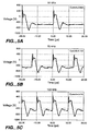
- Figures 4A - 4C show the effect on pulse waveform of setting up the power supply so that the power supply is on positive potential for different amounts of time.
- the pulse width is 2 ⁇ -seconds
- the pulse width is 4 ⁇ -seconds
- the pulse width is 8 ⁇ -seconds.
- Such response is target and cathode dependent, so that although the same response qualitatively can be expected for other target and cathode configurations, the magnitude of the voltages (both the positive and the negative spikes and steady state values) may be different than those shown.
- the magnitude of the negative voltage spike affects the deposited carbon film. It has been found that a lower magnitude negative voltage spike results in films with less sp 3 content, and conversely a greater magnitude spike results in a greater sp 3 content. While a greater pulse width leads to a greater negative voltage spike, it also results in a reduced duty cycle meaning that an embodiment such as that shown in Figure 4C will have a lower sputter rate than the embodiment of Figure 4A .
- the pulsed power supply with the high voltage swings such as the ENI's RPG model can be also set up to run at different frequencies.
- the power supply can be set up to run at frequencies higher than 50 kHz.
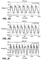
- Figures 5A - 5I are a series of graphs showing the effect on pulse waveform as a function of pulse frequency from 50 to 250 kHz, as indicated in the Figures.
- the width of the positive swing has been kept constant at around 2 ⁇ -seconds in each case. It can be seen that in this set up, the value of the negative voltage spike remains roughly the same across all the frequency ranges.
- the duty cycle can be adjusted as shown in Figures 4A - 4C as long as there is enough time to fit the length of the pulse within the frequency value that was chosen.
- the power supply can be set up in different configurations for which the characteristics as described in Figure 2 can be obtained.
- the frequency increases the negative voltage spike makes up a larger and larger portion of the off cycle.
- the steady state portion of the on cycle begins to disappear. Nevertheless, as can be seen a large spike exists which is greater in magnitude than the average voltage during the on cycle.
- the films were sputtered using the above-described RPG pulsed power supply from ENI in an in-line deposition tool manufactured by Ulvac Inc. of Japan.
- the disks were 95mm diameter and 0.8mm thick aluminum plated with NiP.
- 15 nm of Cr alloy underlayer was coated, followed by 15 nm thick CoCrTaPt magnetic layer.
- the carbon was sputtered at different power settings ranging from 2.0 KWatts to 4.0 KWatts to obtain film thickness that range from 5 to 10 nm in thickness.
- An argon flow of 45 sccm and hydrogen flow of approximately 20 sccm was used during sputtering.
- the pressure was maintained at approximately 0.33Pa (2.5 milli-Torr) during sputtering.
- the carbon target dimension was 23 x 62 cm.
- the approximate deposition rate for above thickness range is between 0.13 to 0.26 nm/second.
- the power supply was set to 50 kHz for a pulse length of 20 ⁇ -seconds.
- the positive voltage swing duration (pulse width) was set to 2 ⁇ -seconds. Pallets carrying the disks were moving by the carbon target at around 40 cm per minute.
- the carbon target was a conventional graphite target as is available from many sources. It will be appreciated that the above parameters, including power supply parameters, and process parameters may be varied and that the foregoing are merely exemplary. Additionally, in embodiments where it is desired to form a hydrogenated film, either hydrogen or hydrogen containing gases such as ethylene, acetylene, butane, naphthalene and others may be used.
- Figure 6 is a data obtained from reflection energy loss spectrometer (REELS) for carbon films made by three different deposition methods.
- REELS reflection energy loss spectrometer
- the first film, shown by trace 601 is a conventionally sputtered carbon film
- the second film, shown by trace 602 is a PE-CVD film
- the third film, shown by trace 603, is a film sputtered according to the method of the present invention described above.
- the ion beam deposited film was made by a decomposition of acetylene gas in the ion beam plasma, in a known process to create a film with a high fraction of sp 3 content.
- Reflection electron energy loss spectroscopy is an well-accepted spectroscopy method which can probe the chemical bonding structure of materials. It is particularly well suited for the analysis of carbon films for determining the nature of the bonding present between the atoms, and also can provide an estimate of the fraction of the bonding that is sp 3 .
- the plot also shows the spectra for graphite (trace 604) to illustrate what the spectra for an sp2 material looks like.
- the figure shows that a conventionally sputtered film is set apart from the other two, and that a PE-CVD film and a film made according to the above-described embodiment have very similar characteristics.
- Analysis of the spectrum by known methods indicates that conventionally sputtered film has 50% sp 3 bonding, while the PE-CVD film has 70% sp 3 and the film made by the present invention has 72% sp 3 content.
- the high value of sp 3 content is a good indicator of formation of ta-C:H type of film by the new sputtering method.
- a second indicator of ta-C:H character of a carbon film is the film stress.
- Film stress is measured by measuring the deflection of the actual disk material as result of depositing the film in question on only one side. The disk is pre-measured for flatness and after deposition on one side, the disk deflects in response to the stress of the film. By measuring the deflection using a sensitive optical tool, film stress can be determined. It is known from scientific studies on carbon films that film stress is well-correlated to the sp 3 content of the film. Higher sp 3 content film has higher stress for a given thickness of film.
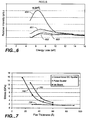
- Figure 7 shows a comparison of three different types of films for film stress as function of film thickness.
- the comparison is between a conventional DC sputtered carbon film (trace 701), an ion-beam deposited film that is known to have high sp 3 content (trace 702), and a pulse sputtered carbon film made according to the present invention (trace 703).
- both ion-beam and the invented sputtered film have similar characteristics with film thickness, namely the stress level rapidly increase as film thickness is reduced, so that by 3 nm thickness for example, both ion-beam and film sputtered by new method has substantially higher stress compared to conventionally sputtered carbon film.
- This result is again indicative of high sp 3 content in the film and shows that films deposited by the method of the present invention are equal to if not superior to ion-beam deposited carbon films.
- Figure 8 is a comparison of Raman spectroscopy analysis of Id/Ig ratio of three types of carbon films at 4 nm thickness.
- Raman spectroscopy is a conventionally accepted means of analyzing the chemistry of carbon films.
- Characterization of Diamond Films by Raman Spectroscopy by D. Knight et al. in Journal of Materials Research, Vol. 4, No. 2, March/April 1989 .
- the Raman spectrum is characterized by broad absorption peaks that are roughly centered on two wavelengths. The peaks are identified as “d” and "g” peaks, and it is known that the ratio of these intensities are indirect indicator of sp 3 content in the film.
- Another indicator of the characteristics of a carbon film is its ability to protect the disk from corrosion.
- One way to measure such property of the film is to conduct ion extraction from the disk surface. This is accomplished by first exposing a disk to high temperature and humidity for some period of time to attempt to cause corrosion of the cobalt containing magnetic layer. For example, the disk may be exposed to a temperature of 60°C at 80% relative humidity for 96 hours. If some amount of corrosion occurs, the cobalt is known to migrate to the surface of the disk as it oxidizes and form cobalt oxide corrosion by-product. This is an extremely sensitive measure of the corrosion susceptibility of the media. This cobalt is then washed off by water, and the water is analyzed for presence of cobalt ions using ion chromatography.
- the method is extremely sensitive, which allows detection of only a few micro-grams of ions per given square meter of surface analyzed. If the overcoat has less ability to protect the film from corrosion, a greater amount of cobalt leaches out during the high temperature and humidity exposure.
- Figure 9 shows the result of ion-extraction results for three types of carbon films, at 5 nm thickness on a 95mm media. It shows that ion beam carbon 902 has extractable cobalt of less than 1 ⁇ g/m2, conventional DC sputtered carbon 901 has extractable cobalt of around 5 ⁇ g/m2 and pulse sputtered carbon 903 according to the present invention has extractable cobalt of around 1.5 ⁇ g/m2.
- the corrosion resistance of the present invention may be considered equivalent to the ion beam carbon given the variability in the measurement, and it is clearly set apart from the conventionally sputtered carbon film.
- the values obtained for both ion beam and pulse sputtered carbon films are considered extremely low in comparison to the values typically obtained for conventionally sputtered films.
- a film deposited according to the present invention clearly has considerable advantage over the conventionally sputtered carbon due to a greater ability to protect the magnetic layer from corrosion.
- the carbon films were also tested by an abrasive wear test to determine the relative durability of the overcoat.
- the test consists of passing abrasive tape over the disk for a fixed length of time, followed by an optical intensity scan to determine the amount of damage inflicted on the disk.
- the measurement is a relative measure and designed to reflect the mechanical durability of the film to intense abrasive wear condition. A lower value is better.
- Table 1 shows a tabulation of several types of films tested. Of note is the comparison between the pulse sputtered carbon at 8nm against conventionally sputtered carbon at 10 and 11.5 nm thickness.
- the pulse sputtered carbon has a result which is comparable to thicker carbon film indicating an improvement in wear resistance compared to the conventionally sputtered film.
- Table 1 Sample Type Carbon thickness Scratch Level Conventional Sputter 11.5 nm 40
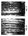
- FIG. 10 shows a photograph of the DC magnetron target used in the Ulvac in-line tool after two weeks of continuous operation using conventional DC magnetron sputtering.
- the target surface is full of nodules which have been described in U.S. Patent No. 5,507,930 . These features are associated with formation of defects on the disk, and also with the formation of particulates during deposition.
- Figure 11 shows the same cathode after 2 weeks of deposition using pulse sputtering at 50 kHz.
- the target surface is remarkably clean compared to Figure 10 .
- This method then is clearly superior to any PE-CVD or ion-beam deposition method in terms of cleanliness of the process. Yield and quality of the disk is expected to be like-wise superior compared to conventional sputter process.
- the properties of the pulse sputtered film can be further enhanced and controlled through application of negative substrate bias during the pulse sputtering.
- Trace 1201 of Figure 12 shows the results of different substrate bias on the stress of the 5 nm thick carbon films, deposited with heating such that the substrate temperature was approximately 98°C during sputtering. From approximately 30 to 100 volts negative substrate bias, the film stress can be raised from around 3.2 Gpa to 4.5 Gpa. This is a significant increase over the unbiased condition. It is expected that the atomic property of the film is likewise changing to a higher sp 3 fraction by application of such bias.
- the bias can be applied with steady DC bias, or the same pulsed power supply can be used for substrate bias as well.
- bias may range from, e.g., the voltage that builds up on the substrate when it is allowed to float, to approximately 200 volts negative.
- data point 1202 shows the stress of a 4 nm ion beam film deposited at a temperature of approximately 150°C in the earlier described system from Intevac.
- Adjustment of substrate temperature by a small amount at the time of pulse sputtering can also impact the film stress. For example, if the temperature is raised from 97 to 115°C, the film stress can be changed from 3.2 Gpa to about 6.8 Gpa without changing any other parameters. This result is also indicated in Figure 12 by line 1205.
- variables available to adjust the properties of the carbon film include settings used for the pulse power supply (e.g. frequency, power and pulse width), the sputter deposition conditions such as pressure, gas composition and flow rate(s), substrate bias conditions and the substrate temperature.
- the parameters can be adjusted to optimize the carbon films for proper level of sp 3 bonding for optimum contact start stop, or corrosion resistance or other measure of durability as desired for different drive applications.
- the method of the present invention provides an improved magnetic recording disk, which can be used to produce an improved disk drive.
- the disk drive may have one ore more of improved CSS performance, corrosion resistance, durability and defect levels.
- the large negative voltage spike produced by the power supplies described earlier provides for sufficiently high energy carbon or carbon ions such that a high percentage of sp 3 bonding is formed.
- the increased positive voltage spike at the beginning of the off pulse may account for the improvement of the present invention, either alone or in combination with the negative spike.
- the negative spike it is believed that any spike in voltage greater than the steady state value is helpful.
- the spike is approximately 25% greater than the steady state voltage, and more preferably approximately 50% or more greater than the steady state voltage.
- embodiments of the present invention where the spike is approximately 100% or more greater than the steady state voltage are advantageous.
- a true steady state negative voltage may not be reached. Nevertheless, in such embodiments it is believed that a large spike that is greater than the average voltage during the on cycle by approximately the foregoing amounts is beneficial.
- known adjustments can be made to the system to increase the voltage levels. For example, as is known, a weaker magnetic field results in an increased voltage for a given current.
- the high magnitude of the voltage spike is beneficial.
- the negative voltage spike in embodiments of the present invention typically is approximately 900 volts - 1,000 volts or more. This is much greater than the voltage typically used in conventional DC or conventional pulsed DC sputtering processes.
- the steady state negative voltage during the on cycle of a pulsed process is slightly greater than the DC voltage of a continuous DC process having the same sputter rate due to the off portion of the cycle.
- the effect of the off cycle is somewhat reduced by virtue of the fact that a greater amount of sputtering occurs during the negative voltage spike.
- a spike in the range of approximately 900 volts or more, or in relative terms 50% greater and more preferably 100% or more greater than the voltage in a continuous DC process or the steady state voltage in a conventional pulsed DC process having the same sputter rate, is beneficial.
- voltages it will be appreciated that the target and the substrate are usually referenced to ground, and in most systems the chamber walls are grounded.
- the sputtering is typically driven by the voltage difference between the target and the substrate, so that, for example, a negative voltage as used herein does not necessarily mean as referenced to ground, but may be instead the magnitude as referenced to the substrate, for example.
Landscapes
- Chemical & Material Sciences (AREA)
- Chemical Kinetics & Catalysis (AREA)
- Engineering & Computer Science (AREA)
- Materials Engineering (AREA)
- Mechanical Engineering (AREA)
- Metallurgy (AREA)
- Organic Chemistry (AREA)
- Physical Vapour Deposition (AREA)
- Manufacturing Of Magnetic Record Carriers (AREA)
- Carbon And Carbon Compounds (AREA)
Applications Claiming Priority (2)
| Application Number | Priority Date | Filing Date | Title |
|---|---|---|---|
| US09/298,107 US6086730A (en) | 1999-04-22 | 1999-04-22 | Method of sputtering a carbon protective film on a magnetic disk with high sp3 content |
| US298107 | 1999-04-22 |
Publications (3)
| Publication Number | Publication Date |
|---|---|
| EP1046726A2 EP1046726A2 (en) | 2000-10-25 |
| EP1046726A3 EP1046726A3 (en) | 2003-07-23 |
| EP1046726B1 true EP1046726B1 (en) | 2009-07-15 |
Family
ID=23149061
Family Applications (1)
| Application Number | Title | Priority Date | Filing Date |
|---|---|---|---|
| EP00303307A Expired - Lifetime EP1046726B1 (en) | 1999-04-22 | 2000-04-19 | Sputtering method for the formation of carbon films |
Country Status (7)
| Country | Link |
|---|---|
| US (1) | US6086730A (enExample) |
| EP (1) | EP1046726B1 (enExample) |
| JP (1) | JP5022533B2 (enExample) |
| DE (1) | DE60042533D1 (enExample) |
| MY (1) | MY124998A (enExample) |
| SG (1) | SG100616A1 (enExample) |
| TW (1) | TW570991B (enExample) |
Cited By (2)
| Publication number | Priority date | Publication date | Assignee | Title |
|---|---|---|---|---|
| US7808184B2 (en) | 2004-02-22 | 2010-10-05 | Zond, Inc. | Methods and apparatus for generating strongly-ionized plasmas with ionizational instabilities |
| US9771648B2 (en) | 2004-08-13 | 2017-09-26 | Zond, Inc. | Method of ionized physical vapor deposition sputter coating high aspect-ratio structures |
Families Citing this family (124)
| Publication number | Priority date | Publication date | Assignee | Title |
|---|---|---|---|---|
| US6290821B1 (en) * | 1999-07-15 | 2001-09-18 | Seagate Technology Llc | Sputter deposition utilizing pulsed cathode and substrate bias power |
| US6350353B2 (en) * | 1999-11-24 | 2002-02-26 | Applied Materials, Inc. | Alternate steps of IMP and sputtering process to improve sidewall coverage |
| US6565719B1 (en) * | 2000-06-27 | 2003-05-20 | Komag, Inc. | Magnetic disk comprising a first carbon overcoat having a high SP3 content and a second carbon overcoat having a low SP3 content |
| US6902773B1 (en) * | 2000-11-21 | 2005-06-07 | Hitachi Global Storage Technologies Netherlands, B.V. | Energy gradient ion beam deposition of carbon overcoats on rigid disk media for magnetic recordings |
| US6638608B1 (en) | 2001-03-16 | 2003-10-28 | Seagate Technology Llc | Protection overcoat for recording media |
| US20030049496A1 (en) * | 2001-09-11 | 2003-03-13 | Pocker Daryl J. | Thin film protective layer with buffering interface |
| US6875492B1 (en) | 2001-11-15 | 2005-04-05 | Maxtor Corporation | Carbon overcoat for magnetic recording medium |
| US6767592B2 (en) | 2001-12-05 | 2004-07-27 | Seagate Technology Llc | Method for thin film protective overcoat |
| DE10203730B4 (de) * | 2002-01-30 | 2010-09-16 | Fraunhofer-Gesellschaft zur Förderung der angewandten Forschung e.V. | Verfahren zur Abscheidung von metallfreien Kohlenstoffschichten |
| US7378356B2 (en) * | 2002-03-16 | 2008-05-27 | Springworks, Llc | Biased pulse DC reactive sputtering of oxide films |
| US6896773B2 (en) * | 2002-11-14 | 2005-05-24 | Zond, Inc. | High deposition rate sputtering |
| US20040209123A1 (en) * | 2003-04-17 | 2004-10-21 | Bajorek Christopher H. | Method of fabricating a discrete track recording disk using a bilayer resist for metal lift-off |
| US7300556B2 (en) * | 2003-08-29 | 2007-11-27 | Hitachi Global Storage Technologies Netherlands B.V. | Method for depositing a thin film adhesion layer |
| US20050103620A1 (en) * | 2003-11-19 | 2005-05-19 | Zond, Inc. | Plasma source with segmented magnetron cathode |
| US20050150862A1 (en) * | 2004-01-13 | 2005-07-14 | Harper Bruce M. | Workpiece alignment assembly |
| US20050151300A1 (en) * | 2004-01-13 | 2005-07-14 | Harper Bruce M. | Workpiece isothermal imprinting |
| US20050151282A1 (en) * | 2004-01-13 | 2005-07-14 | Harper Bruce M. | Workpiece handler and alignment assembly |
| US7686606B2 (en) * | 2004-01-20 | 2010-03-30 | Wd Media, Inc. | Imprint embossing alignment system |
| US7329114B2 (en) * | 2004-01-20 | 2008-02-12 | Komag, Inc. | Isothermal imprint embossing system |
| US20050155554A1 (en) * | 2004-01-20 | 2005-07-21 | Saito Toshiyuki M. | Imprint embossing system |
| US9123508B2 (en) * | 2004-02-22 | 2015-09-01 | Zond, Llc | Apparatus and method for sputtering hard coatings |
| US20050249983A1 (en) * | 2004-05-06 | 2005-11-10 | Seagate Technology Llc | Thickness gradient protective overcoat layers by filtered cathodic arc deposition |
| EP2477207A3 (en) * | 2004-09-24 | 2014-09-03 | Zond, Inc. | Apparatus for generating high-current electrical discharges |
| US20060278521A1 (en) * | 2005-06-14 | 2006-12-14 | Stowell Michael W | System and method for controlling ion density and energy using modulated power signals |
| US7758982B2 (en) * | 2005-09-02 | 2010-07-20 | Hitachi Global Storage Technologies Netherlands B.V. | SiN overcoat for perpendicular magnetic recording media |
| US8900771B2 (en) * | 2006-08-17 | 2014-12-02 | GM Global Technology Operations LLC | Non-noble metal inexpensive conductive coatings for fuel cell bipolar plates |
| EP1912266A1 (en) * | 2006-10-10 | 2008-04-16 | STMicroelectronics S.r.l. | Method of forming phase change memory devices in a pulsed DC deposition chamber |
| JP2008171505A (ja) * | 2007-01-12 | 2008-07-24 | Showa Denko Kk | 炭素保護膜の形成方法及び磁気記録媒体の製造方法、磁気記録媒体並びに磁気記録再生装置 |
| US20080311012A1 (en) * | 2007-06-12 | 2008-12-18 | Uri Levy | Transmissive window for hydrooptic disinfection system |
| JP5117895B2 (ja) | 2008-03-17 | 2013-01-16 | ダブリュディ・メディア・シンガポール・プライベートリミテッド | 磁気記録媒体及びその製造方法 |
| JP2009238299A (ja) * | 2008-03-26 | 2009-10-15 | Hoya Corp | 垂直磁気記録媒体および垂直磁気記録媒体の製造方法 |
| JP5453666B2 (ja) | 2008-03-30 | 2014-03-26 | ダブリュディ・メディア・シンガポール・プライベートリミテッド | 磁気ディスク及びその製造方法 |
| JP2011034603A (ja) * | 2008-03-31 | 2011-02-17 | Hoya Corp | 垂直磁気記録媒体 |
| WO2010038773A1 (ja) | 2008-09-30 | 2010-04-08 | Hoya株式会社 | 磁気ディスク及びその製造方法 |
| US8877359B2 (en) | 2008-12-05 | 2014-11-04 | Wd Media (Singapore) Pte. Ltd. | Magnetic disk and method for manufacturing same |
| US9558778B2 (en) | 2009-03-28 | 2017-01-31 | Wd Media (Singapore) Pte. Ltd. | Lubricant compound for magnetic disk and magnetic disk |
| SG165294A1 (en) | 2009-03-30 | 2010-10-28 | Wd Media Singapore Pte Ltd | Perpendicular magnetic recording medium and method of manufacturing the same |
| US20100300884A1 (en) | 2009-05-26 | 2010-12-02 | Wd Media, Inc. | Electro-deposited passivation coatings for patterned media |
| US8496466B1 (en) | 2009-11-06 | 2013-07-30 | WD Media, LLC | Press system with interleaved embossing foil holders for nano-imprinting of recording media |
| US8402638B1 (en) | 2009-11-06 | 2013-03-26 | Wd Media, Inc. | Press system with embossing foil free to expand for nano-imprinting of recording media |
| US9330685B1 (en) | 2009-11-06 | 2016-05-03 | WD Media, LLC | Press system for nano-imprinting of recording media with a two step pressing method |
| JP5643516B2 (ja) * | 2010-01-08 | 2014-12-17 | ダブリュディ・メディア・シンガポール・プライベートリミテッド | 垂直磁気記録媒体 |
| JP5574414B2 (ja) | 2010-03-29 | 2014-08-20 | ダブリュディ・メディア・シンガポール・プライベートリミテッド | 磁気ディスクの評価方法及び磁気ディスクの製造方法 |
| JP5762101B2 (ja) * | 2010-04-14 | 2015-08-12 | キヤノン株式会社 | 光学素子成形用型の製造方法および光学素子成形用型 |
| TW201137149A (en) * | 2010-04-21 | 2011-11-01 | Hon Hai Prec Ind Co Ltd | Magnetron sputtering device |
| CN102234776A (zh) * | 2010-04-22 | 2011-11-09 | 鸿富锦精密工业(深圳)有限公司 | 磁控溅镀装置 |
| JP5645476B2 (ja) | 2010-05-21 | 2014-12-24 | ダブリュディ・メディア・シンガポール・プライベートリミテッド | 垂直磁気ディスク |
| JP5634749B2 (ja) | 2010-05-21 | 2014-12-03 | ダブリュディ・メディア・シンガポール・プライベートリミテッド | 垂直磁気ディスク |
| JP2011248969A (ja) | 2010-05-28 | 2011-12-08 | Wd Media (Singapore) Pte. Ltd | 垂直磁気ディスク |
| JP2011248968A (ja) | 2010-05-28 | 2011-12-08 | Wd Media (Singapore) Pte. Ltd | 垂直磁気ディスク |
| JP2011248967A (ja) | 2010-05-28 | 2011-12-08 | Wd Media (Singapore) Pte. Ltd | 垂直磁気ディスクの製造方法 |
| JP2012009086A (ja) | 2010-06-22 | 2012-01-12 | Wd Media (Singapore) Pte. Ltd | 垂直磁気記録媒体及びその製造方法 |
| US8889275B1 (en) | 2010-08-20 | 2014-11-18 | WD Media, LLC | Single layer small grain size FePT:C film for heat assisted magnetic recording media |
| US8743666B1 (en) | 2011-03-08 | 2014-06-03 | Western Digital Technologies, Inc. | Energy assisted magnetic recording medium capable of suppressing high DC readback noise |
| US9139902B2 (en) * | 2011-03-10 | 2015-09-22 | Korea Institute Of Science And Technology | Method and apparatus for plasma ion implantation of solid element |
| US8711499B1 (en) | 2011-03-10 | 2014-04-29 | WD Media, LLC | Methods for measuring media performance associated with adjacent track interference |
| US8491800B1 (en) | 2011-03-25 | 2013-07-23 | WD Media, LLC | Manufacturing of hard masks for patterning magnetic media |
| US9028985B2 (en) | 2011-03-31 | 2015-05-12 | WD Media, LLC | Recording media with multiple exchange coupled magnetic layers |
| EP2587518B1 (en) * | 2011-10-31 | 2018-12-19 | IHI Hauzer Techno Coating B.V. | Apparatus and Method for depositing Hydrogen-free ta C Layers on Workpieces and Workpiece |
| WO2013075061A1 (en) * | 2011-11-17 | 2013-05-23 | United Protective Technologies | Carbon based coatings and methods of producing the same |
| US8565050B1 (en) | 2011-12-20 | 2013-10-22 | WD Media, LLC | Heat assisted magnetic recording media having moment keeper layer |
| US9029308B1 (en) | 2012-03-28 | 2015-05-12 | WD Media, LLC | Low foam media cleaning detergent |
| US9269480B1 (en) | 2012-03-30 | 2016-02-23 | WD Media, LLC | Systems and methods for forming magnetic recording media with improved grain columnar growth for energy assisted magnetic recording |
| US8941950B2 (en) | 2012-05-23 | 2015-01-27 | WD Media, LLC | Underlayers for heat assisted magnetic recording (HAMR) media |
| US8993134B2 (en) | 2012-06-29 | 2015-03-31 | Western Digital Technologies, Inc. | Electrically conductive underlayer to grow FePt granular media with (001) texture on glass substrates |
| US9034492B1 (en) | 2013-01-11 | 2015-05-19 | WD Media, LLC | Systems and methods for controlling damping of magnetic media for heat assisted magnetic recording |
| US10115428B1 (en) | 2013-02-15 | 2018-10-30 | Wd Media, Inc. | HAMR media structure having an anisotropic thermal barrier layer |
| US9153268B1 (en) | 2013-02-19 | 2015-10-06 | WD Media, LLC | Lubricants comprising fluorinated graphene nanoribbons for magnetic recording media structure |
| US9183867B1 (en) | 2013-02-21 | 2015-11-10 | WD Media, LLC | Systems and methods for forming implanted capping layers in magnetic media for magnetic recording |
| US9196283B1 (en) | 2013-03-13 | 2015-11-24 | Western Digital (Fremont), Llc | Method for providing a magnetic recording transducer using a chemical buffer |
| US8787130B1 (en) | 2013-03-15 | 2014-07-22 | WD Media, LLC | Systems and methods for providing heat assisted magnetic recording media configured to couple energy from a near field transducer |
| US9190094B2 (en) | 2013-04-04 | 2015-11-17 | Western Digital (Fremont) | Perpendicular recording media with grain isolation initiation layer and exchange breaking layer for signal-to-noise ratio enhancement |
| US9093122B1 (en) | 2013-04-05 | 2015-07-28 | WD Media, LLC | Systems and methods for improving accuracy of test measurements involving aggressor tracks written to disks of hard disk drives |
| US8947987B1 (en) | 2013-05-03 | 2015-02-03 | WD Media, LLC | Systems and methods for providing capping layers for heat assisted magnetic recording media |
| US8867322B1 (en) | 2013-05-07 | 2014-10-21 | WD Media, LLC | Systems and methods for providing thermal barrier bilayers for heat assisted magnetic recording media |
| US9296082B1 (en) | 2013-06-11 | 2016-03-29 | WD Media, LLC | Disk buffing apparatus with abrasive tape loading pad having a vibration absorbing layer |
| US9406330B1 (en) | 2013-06-19 | 2016-08-02 | WD Media, LLC | Method for HDD disk defect source detection |
| US9607646B2 (en) | 2013-07-30 | 2017-03-28 | WD Media, LLC | Hard disk double lubrication layer |
| US9389135B2 (en) | 2013-09-26 | 2016-07-12 | WD Media, LLC | Systems and methods for calibrating a load cell of a disk burnishing machine |
| US9177585B1 (en) | 2013-10-23 | 2015-11-03 | WD Media, LLC | Magnetic media capable of improving magnetic properties and thermal management for heat-assisted magnetic recording |
| US9581510B1 (en) | 2013-12-16 | 2017-02-28 | Western Digital Technologies, Inc. | Sputter chamber pressure gauge with vibration absorber |
| US9382496B1 (en) | 2013-12-19 | 2016-07-05 | Western Digital Technologies, Inc. | Lubricants with high thermal stability for heat-assisted magnetic recording |
| US20170051396A1 (en) * | 2014-02-12 | 2017-02-23 | Ulvac, Inc. | Method for Forming Carbon Electrode Film, Carbon Electrode, and Method for Manufacturing Phase Change Memory Element |
| US9824711B1 (en) | 2014-02-14 | 2017-11-21 | WD Media, LLC | Soft underlayer for heat assisted magnetic recording media |
| US9447368B1 (en) | 2014-02-18 | 2016-09-20 | WD Media, LLC | Detergent composition with low foam and high nickel solubility |
| US9431045B1 (en) | 2014-04-25 | 2016-08-30 | WD Media, LLC | Magnetic seed layer used with an unbalanced soft underlayer |
| US9984915B2 (en) * | 2014-05-30 | 2018-05-29 | Infineon Technologies Ag | Semiconductor wafer and method for processing a semiconductor wafer |
| US9042053B1 (en) | 2014-06-24 | 2015-05-26 | WD Media, LLC | Thermally stabilized perpendicular magnetic recording medium |
| US9159350B1 (en) | 2014-07-02 | 2015-10-13 | WD Media, LLC | High damping cap layer for magnetic recording media |
| US10054363B2 (en) | 2014-08-15 | 2018-08-21 | WD Media, LLC | Method and apparatus for cryogenic dynamic cooling |
| US9082447B1 (en) | 2014-09-22 | 2015-07-14 | WD Media, LLC | Determining storage media substrate material type |
| US8995078B1 (en) | 2014-09-25 | 2015-03-31 | WD Media, LLC | Method of testing a head for contamination |
| US9227324B1 (en) | 2014-09-25 | 2016-01-05 | WD Media, LLC | Mandrel for substrate transport system with notch |
| US9685184B1 (en) | 2014-09-25 | 2017-06-20 | WD Media, LLC | NiFeX-based seed layer for magnetic recording media |
| US9449633B1 (en) | 2014-11-06 | 2016-09-20 | WD Media, LLC | Smooth structures for heat-assisted magnetic recording media |
| US9818442B2 (en) | 2014-12-01 | 2017-11-14 | WD Media, LLC | Magnetic media having improved magnetic grain size distribution and intergranular segregation |
| US9401300B1 (en) | 2014-12-18 | 2016-07-26 | WD Media, LLC | Media substrate gripper including a plurality of snap-fit fingers |
| US9218850B1 (en) | 2014-12-23 | 2015-12-22 | WD Media, LLC | Exchange break layer for heat-assisted magnetic recording media |
| US9257134B1 (en) | 2014-12-24 | 2016-02-09 | Western Digital Technologies, Inc. | Allowing fast data zone switches on data storage devices |
| US9990940B1 (en) | 2014-12-30 | 2018-06-05 | WD Media, LLC | Seed structure for perpendicular magnetic recording media |
| US9280998B1 (en) | 2015-03-30 | 2016-03-08 | WD Media, LLC | Acidic post-sputter wash for magnetic recording media |
| US9822441B2 (en) | 2015-03-31 | 2017-11-21 | WD Media, LLC | Iridium underlayer for heat assisted magnetic recording media |
| US9275669B1 (en) | 2015-03-31 | 2016-03-01 | WD Media, LLC | TbFeCo in PMR media for SNR improvement |
| US11074934B1 (en) | 2015-09-25 | 2021-07-27 | Western Digital Technologies, Inc. | Heat assisted magnetic recording (HAMR) media with Curie temperature reduction layer |
| US10236026B1 (en) | 2015-11-06 | 2019-03-19 | WD Media, LLC | Thermal barrier layers and seed layers for control of thermal and structural properties of HAMR media |
| US9406329B1 (en) | 2015-11-30 | 2016-08-02 | WD Media, LLC | HAMR media structure with intermediate layer underlying a magnetic recording layer having multiple sublayers |
| US9858951B1 (en) | 2015-12-01 | 2018-01-02 | Western Digital (Fremont), Llc | Method for providing a multilayer AFM layer in a read sensor |
| US10121506B1 (en) | 2015-12-29 | 2018-11-06 | WD Media, LLC | Magnetic-recording medium including a carbon overcoat implanted with nitrogen and hydrogen |
| US11824454B2 (en) * | 2016-06-21 | 2023-11-21 | Eagle Harbor Technologies, Inc. | Wafer biasing in a plasma chamber |
| US11004660B2 (en) | 2018-11-30 | 2021-05-11 | Eagle Harbor Technologies, Inc. | Variable output impedance RF generator |
| US10858727B2 (en) * | 2016-08-19 | 2020-12-08 | Applied Materials, Inc. | High density, low stress amorphous carbon film, and process and equipment for its deposition |
| US10224224B2 (en) | 2017-03-10 | 2019-03-05 | Micromaterials, LLC | High pressure wafer processing systems and related methods |
| US10622214B2 (en) | 2017-05-25 | 2020-04-14 | Applied Materials, Inc. | Tungsten defluorination by high pressure treatment |
| KR102405723B1 (ko) | 2017-08-18 | 2022-06-07 | 어플라이드 머티어리얼스, 인코포레이티드 | 고압 및 고온 어닐링 챔버 |
| US10276411B2 (en) | 2017-08-18 | 2019-04-30 | Applied Materials, Inc. | High pressure and high temperature anneal chamber |
| CN111357090B (zh) | 2017-11-11 | 2024-01-05 | 微材料有限责任公司 | 用于高压处理腔室的气体输送系统 |
| WO2019099255A2 (en) | 2017-11-17 | 2019-05-23 | Applied Materials, Inc. | Condenser system for high pressure processing system |
| WO2019173006A1 (en) | 2018-03-09 | 2019-09-12 | Applied Materials, Inc. | High pressure annealing process for metal containing materials |
| US10950429B2 (en) * | 2018-05-08 | 2021-03-16 | Applied Materials, Inc. | Methods of forming amorphous carbon hard mask layers and hard mask layers formed therefrom |
| US10748783B2 (en) | 2018-07-25 | 2020-08-18 | Applied Materials, Inc. | Gas delivery module |
| US12456604B2 (en) | 2019-12-24 | 2025-10-28 | Eagle Harbor Technologies, Inc. | Nanosecond pulser RF isolation for plasma systems |
| WO2020117462A1 (en) | 2018-12-07 | 2020-06-11 | Applied Materials, Inc. | Semiconductor processing system |
| US11270872B2 (en) | 2019-09-25 | 2022-03-08 | Western Digital Technologies, Inc. | Base conducting layer beneath graphite layer of ceramic cathode for use with cathodic arc deposition |
| US11901222B2 (en) | 2020-02-17 | 2024-02-13 | Applied Materials, Inc. | Multi-step process for flowable gap-fill film |
Family Cites Families (19)
| Publication number | Priority date | Publication date | Assignee | Title |
|---|---|---|---|---|
| JP2600297B2 (ja) * | 1988-06-23 | 1997-04-16 | 松下電器産業株式会社 | 磁気記録媒体 |
| US5045165A (en) * | 1990-02-01 | 1991-09-03 | Komag, Inc. | Method for sputtering a hydrogen-doped carbon protective film on a magnetic disk |
| JPH04195715A (ja) * | 1990-11-26 | 1992-07-15 | Tokin Corp | 垂直磁気記録媒体 |
| JPH05143972A (ja) * | 1991-11-19 | 1993-06-11 | Kubota Corp | 金属薄膜型磁気記録媒体およびその製造法 |
| JPH06145975A (ja) * | 1992-03-20 | 1994-05-27 | Komag Inc | 炭素フィルムをスパタリングする方法及びその製造物 |
| JPH07210865A (ja) * | 1994-01-21 | 1995-08-11 | Matsushita Electric Ind Co Ltd | 磁気記録媒体の製造方法 |
| US5651865A (en) | 1994-06-17 | 1997-07-29 | Eni | Preferential sputtering of insulators from conductive targets |
| JP3934697B2 (ja) * | 1994-12-06 | 2007-06-20 | 昭和電工株式会社 | 磁気記録媒体 |
| JPH0944844A (ja) * | 1995-07-27 | 1997-02-14 | Hitachi Ltd | 磁気記録媒体の製造方法 |
| JPH09288818A (ja) * | 1996-04-22 | 1997-11-04 | Hitachi Metals Ltd | 磁気記録媒体 |
| WO1997045834A1 (en) * | 1996-05-31 | 1997-12-04 | Akashic Memories Corporation | Recording media having protective overcoats of highly tetrahedral amorphous carbon and methods for their production |
| US5858477A (en) * | 1996-12-10 | 1999-01-12 | Akashic Memories Corporation | Method for producing recording media having protective overcoats of highly tetrahedral amorphous carbon |
| JPH101305A (ja) * | 1996-06-11 | 1998-01-06 | Denki Kagaku Kogyo Kk | 炭素膜および炭素膜製造方法 |
| JPH10172130A (ja) * | 1996-12-09 | 1998-06-26 | Hitachi Ltd | 磁気記録媒体及びその製造方法並びに磁気記憶装置 |
| US6245417B1 (en) * | 1997-07-10 | 2001-06-12 | Seagate Technology Llc | Magnetic recording medium comprising multilayered carbon-containing protective overcoats |
| JPH1139647A (ja) * | 1997-07-23 | 1999-02-12 | Hitachi Ltd | 磁気記録媒体及びその製造方法並びに磁気記憶装置 |
| JP3192109B2 (ja) * | 1997-08-07 | 2001-07-23 | 株式会社半導体エネルギー研究所 | 電気用部材 |
| WO1999014746A1 (en) * | 1997-09-17 | 1999-03-25 | Showa Denko K.K. | Magnetic recording medium and method of producing the same |
| US5873984A (en) * | 1997-11-05 | 1999-02-23 | Trace Storage Tech. Corp. | Method of sputtering an amorphous carbon overcoat as a protective film on magnetic recording disk |
-
1999
- 1999-04-22 US US09/298,107 patent/US6086730A/en not_active Expired - Lifetime
-
2000
- 2000-04-18 SG SG200002193A patent/SG100616A1/en unknown
- 2000-04-19 DE DE60042533T patent/DE60042533D1/de not_active Expired - Lifetime
- 2000-04-19 EP EP00303307A patent/EP1046726B1/en not_active Expired - Lifetime
- 2000-04-20 MY MYPI20001698A patent/MY124998A/en unknown
- 2000-04-21 TW TW089107572A patent/TW570991B/zh not_active IP Right Cessation
- 2000-04-24 JP JP2000122444A patent/JP5022533B2/ja not_active Expired - Fee Related
Cited By (2)
| Publication number | Priority date | Publication date | Assignee | Title |
|---|---|---|---|---|
| US7808184B2 (en) | 2004-02-22 | 2010-10-05 | Zond, Inc. | Methods and apparatus for generating strongly-ionized plasmas with ionizational instabilities |
| US9771648B2 (en) | 2004-08-13 | 2017-09-26 | Zond, Inc. | Method of ionized physical vapor deposition sputter coating high aspect-ratio structures |
Also Published As
| Publication number | Publication date |
|---|---|
| JP2000331336A (ja) | 2000-11-30 |
| JP5022533B2 (ja) | 2012-09-12 |
| EP1046726A3 (en) | 2003-07-23 |
| EP1046726A2 (en) | 2000-10-25 |
| SG100616A1 (en) | 2003-12-26 |
| DE60042533D1 (de) | 2009-08-27 |
| US6086730A (en) | 2000-07-11 |
| TW570991B (en) | 2004-01-11 |
| MY124998A (en) | 2006-07-31 |
Similar Documents
| Publication | Publication Date | Title |
|---|---|---|
| EP1046726B1 (en) | Sputtering method for the formation of carbon films | |
| US6682807B2 (en) | Magnetic disk comprising a first carbon overcoat having a high SP3 content and a second carbon overcoat having a low SP3 content | |
| EP0561641B1 (en) | Method of sputtering a carbon protective film on a magnetic disk by superimposing an AC voltage on a DC bias voltage | |
| US6338777B1 (en) | Method and apparatus for sputtering thin films | |
| US5679431A (en) | Sputtered carbon overcoat in a thin-film medium and sputtering method | |
| US8865269B2 (en) | Method of forming a protective film for a magnetic recording medium, a protective film formed by the method and a magnetic recording medium having the protective film | |
| US5942317A (en) | Hydrogenated carbon thin films | |
| US5901021A (en) | Thin-film magnetic head | |
| KR19990029033A (ko) | 자기 디스크용 다중상 보호코팅 | |
| CN101236747A (zh) | 包括氮氧化铝衬层和类金刚石覆层的磁记录头和介质 | |
| US6835290B2 (en) | System and method for controlling thin film defects | |
| US7147943B2 (en) | Magnetic recording medium, the manufacturing method and magnetic recording apparatus using the same | |
| US7153441B2 (en) | Method for manufacturing thin-film magnetic recording medium | |
| US6268036B1 (en) | Thin film disk with highly faulted crystalline underlayer | |
| US6403194B1 (en) | Magnetic recording medium, process for producing same and magnetic disc apparatus | |
| JP4193320B2 (ja) | 磁気記録媒体の製造方法 | |
| US6969447B2 (en) | Thin film protective layer with buffering interface | |
| EP1381703B1 (en) | A method for determining a critical size of an inclusion in aluminum or aluminum alloy sputtering target | |
| JPH10326406A (ja) | 磁気ヘッドスライダおよびその製造方法 | |
| US6419993B1 (en) | Production process for magnetic recording medium | |
| US20060153975A1 (en) | Magnetic recording medium, the manufacturing method and magnetic recording apparatus using the same | |
| Lu | Sputtering deposition and characterization of ultrathin amorphous carbon films | |
| Matlak et al. | Friction of Ultrathin Amorphous Carbon Films Synthesized by Filtered Cathodic Vacuum Arc and Radio-Frequency Sputtering | |
| HK1009202B (en) | Multi-phase overcoats for magnetic discs | |
| JPH0690790B2 (ja) | 磁気記録媒体の製造方法 |
Legal Events
| Date | Code | Title | Description |
|---|---|---|---|
| PUAI | Public reference made under article 153(3) epc to a published international application that has entered the european phase |
Free format text: ORIGINAL CODE: 0009012 |
|
| AK | Designated contracting states |
Kind code of ref document: A2 Designated state(s): AT BE CH CY DE DK ES FI FR GB GR IE IT LI LU MC NL PT SE |
|
| AX | Request for extension of the european patent |
Free format text: AL;LT;LV;MK;RO;SI |
|
| RIN1 | Information on inventor provided before grant (corrected) |
Inventor name: YAMASHITA, TSUTOMU Inventor name: PENG, GANG Inventor name: LIU, WEN HONG Inventor name: CHEN, TU |
|
| PUAL | Search report despatched |
Free format text: ORIGINAL CODE: 0009013 |
|
| AK | Designated contracting states |
Designated state(s): AT BE CH CY DE DK ES FI FR GB GR IE IT LI LU MC NL PT SE |
|
| AX | Request for extension of the european patent |
Extension state: AL LT LV MK RO SI |
|
| 17P | Request for examination filed |
Effective date: 20031121 |
|
| AKX | Designation fees paid |
Designated state(s): DE |
|
| 17Q | First examination report despatched |
Effective date: 20080903 |
|
| GRAP | Despatch of communication of intention to grant a patent |
Free format text: ORIGINAL CODE: EPIDOSNIGR1 |
|
| GRAS | Grant fee paid |
Free format text: ORIGINAL CODE: EPIDOSNIGR3 |
|
| GRAA | (expected) grant |
Free format text: ORIGINAL CODE: 0009210 |
|
| AK | Designated contracting states |
Kind code of ref document: B1 Designated state(s): DE |
|
| REF | Corresponds to: |
Ref document number: 60042533 Country of ref document: DE Date of ref document: 20090827 Kind code of ref document: P |
|
| PLBE | No opposition filed within time limit |
Free format text: ORIGINAL CODE: 0009261 |
|
| STAA | Information on the status of an ep patent application or granted ep patent |
Free format text: STATUS: NO OPPOSITION FILED WITHIN TIME LIMIT |
|
| 26N | No opposition filed |
Effective date: 20100416 |
|
| REG | Reference to a national code |
Ref country code: DE Ref legal event code: R082 Ref document number: 60042533 Country of ref document: DE Representative=s name: KOTITSCHKE & HEURUNG PARTNERSCHAFT MBB PATENT-, DE Ref country code: DE Ref legal event code: R082 Ref document number: 60042533 Country of ref document: DE Representative=s name: KOTITSCHKE & HEURUNG PARTNERSCHAFT MBB, DE |
|
| PGFP | Annual fee paid to national office [announced via postgrant information from national office to epo] |
Ref country code: DE Payment date: 20140429 Year of fee payment: 15 |
|
| REG | Reference to a national code |
Ref country code: DE Ref legal event code: R119 Ref document number: 60042533 Country of ref document: DE |
|
| PG25 | Lapsed in a contracting state [announced via postgrant information from national office to epo] |
Ref country code: DE Free format text: LAPSE BECAUSE OF NON-PAYMENT OF DUE FEES Effective date: 20151103 |