EP1038390B1 - High speed readout architecture for analog storage arrays - Google Patents
High speed readout architecture for analog storage arrays Download PDFInfo
- Publication number
- EP1038390B1 EP1038390B1 EP98958504A EP98958504A EP1038390B1 EP 1038390 B1 EP1038390 B1 EP 1038390B1 EP 98958504 A EP98958504 A EP 98958504A EP 98958504 A EP98958504 A EP 98958504A EP 1038390 B1 EP1038390 B1 EP 1038390B1
- Authority
- EP
- European Patent Office
- Prior art keywords
- cell
- signal
- pair
- array
- analog
- Prior art date
- Legal status (The legal status is an assumption and is not a legal conclusion. Google has not performed a legal analysis and makes no representation as to the accuracy of the status listed.)
- Expired - Lifetime
Links
Images



Classifications
-
- H—ELECTRICITY
- H04—ELECTRIC COMMUNICATION TECHNIQUE
- H04N—PICTORIAL COMMUNICATION, e.g. TELEVISION
- H04N3/00—Scanning details of television systems; Combination thereof with generation of supply voltages
- H04N3/10—Scanning details of television systems; Combination thereof with generation of supply voltages by means not exclusively optical-mechanical
- H04N3/14—Scanning details of television systems; Combination thereof with generation of supply voltages by means not exclusively optical-mechanical by means of electrically scanned solid-state devices
-
- H—ELECTRICITY
- H04—ELECTRIC COMMUNICATION TECHNIQUE
- H04N—PICTORIAL COMMUNICATION, e.g. TELEVISION
- H04N25/00—Circuitry of solid-state image sensors [SSIS]; Control thereof
- H04N25/60—Noise processing, e.g. detecting, correcting, reducing or removing noise
- H04N25/616—Noise processing, e.g. detecting, correcting, reducing or removing noise involving a correlated sampling function, e.g. correlated double sampling [CDS] or triple sampling
-
- H—ELECTRICITY
- H04—ELECTRIC COMMUNICATION TECHNIQUE
- H04N—PICTORIAL COMMUNICATION, e.g. TELEVISION
- H04N25/00—Circuitry of solid-state image sensors [SSIS]; Control thereof
- H04N25/70—SSIS architectures; Circuits associated therewith
- H04N25/71—Charge-coupled device [CCD] sensors; Charge-transfer registers specially adapted for CCD sensors
- H04N25/713—Transfer or readout registers; Split readout registers or multiple readout registers
-
- H—ELECTRICITY
- H04—ELECTRIC COMMUNICATION TECHNIQUE
- H04N—PICTORIAL COMMUNICATION, e.g. TELEVISION
- H04N25/00—Circuitry of solid-state image sensors [SSIS]; Control thereof
- H04N25/70—SSIS architectures; Circuits associated therewith
- H04N25/76—Addressed sensors, e.g. MOS or CMOS sensors
- H04N25/78—Readout circuits for addressed sensors, e.g. output amplifiers or A/D converters
-
- H—ELECTRICITY
- H04—ELECTRIC COMMUNICATION TECHNIQUE
- H04N—PICTORIAL COMMUNICATION, e.g. TELEVISION
- H04N25/00—Circuitry of solid-state image sensors [SSIS]; Control thereof
- H04N25/70—SSIS architectures; Circuits associated therewith
- H04N25/76—Addressed sensors, e.g. MOS or CMOS sensors
Definitions
- This invention is generally related to analog signal processing and more particularly to techniques for extracting information from semiconductor storage arrays.
- CMOS complementary metal oxide semiconductor
- Imaging systems that use image arrays include traditional applications such as video cameras and copiers to more modern ones such as the facsimile machine, scanner, medical imaging device, and the digital camera.
- the Article 2 An 800K-Pixel Color CMOS Sensor for Consumer Still Cameras, J.E.D. Hurwitz, P.B. Denyer, D.J. Baxter, and G. Townsend, SPIE Vol. 3019, pages 115-124, describes an image sensor particularly suitable for digital cameras.
- Modem imaging arrays can be very large, having as many as 1024 ⁇ 1024 pixels, with future arrays expected to be even larger. The size is needed to provide detailed images.
- a 1024 ⁇ 1024 array for instance generates over 1 million different analog signals to represent an image frame. The large number of signals thus presents the circuit designer with some problems which need to be addressed in order to improve overall imaging system performance. These include pixel signal readout speed and overall power consumption.
- the readout speed is related to how fast the individual analog signals can be separated from all of the other signals produced by the array, passed through an analog transmission path, and fed to a signal processing pipe.
- imaging arrays and their associated readout circuitry are now being built on the same semiconductor die in order to reduce manufacturing costs. Examples include imaging arrays built using standard complimentary metal oxide semiconductor (CMOS) fabrication processes.
- CMOS complimentary metal oxide semiconductor
- the power dissipated by the readout circuitry heats the pixels. Heating the pixels in turn increases leakage currents within each pixel, and as a result changes pixel response, typically resulting in undesirably brighter and less accurate images. The problem becomes worse in larger arrays if the power dissipated by the readout circuitry is tied to the array size.
- an imaging apparatus as claimed in claim 5 herein.
- one embodiment of the invention is directed at a multi-layer analog signal readout architecture having a storage array and a sense amplifier array feeding an analog multiplexer.
- the sense amp cells of the sense amp array each include an operational amplifier (opamp) pair configured as unity-gain closed loop amplifiers for driving a differential signal pair through the analog multiplexer and into a signal processing pipe.
- the opamps are designed to provide an underdamped response while loaded with the analog transmission path to the signal processing pipe.
- each sense amp cell in the sense amp array is activated in response to either a Select signal or a Select_Ahead signal, or both.
- the Select_Ahead signal activates the cell, and the Select signal permits the cell to drive its differential signal pair into the analog mux. This allows speedy transitioning from one cell to the next as each cell is already activated at the point the Select signal is asserted. Also, maintaining only two cells active at any given time during readout helps reduce power dissipation, and substantially decouples power dissipation in the sense amp array from the size of the array thus making the architecture easily scalable.
- Figure 1 illustrates an architecture for analog signal readout from a storage array 110, according to a first embodiment of the invention.
- the architecture features an array of storage cells that are coupled to a sense amplifier array 114 through a number of output lines (788 are shown as an example). Each output line is coupled to a column of storage cells .
- Analog signals generated by the storage cells are fed to the sense amp array one row at a time through the output lines. Although shown as being read one row at a time, the analog signals can alternatively be read one column at a time, provided of course that each output line is coupled to a row of storage cells rather than a column.
- the sense amp array is a row of sense amplifier cells, one sense amp cell 116 for each column as shown in Figure 1.
- the sense amplifier cells implement correlated double sampling (CDS) of pixel signals.
- CDS as known to those skilled in the art is a technique used to reduce fixed pattern noise in pixel signals. Fixed pattern noise refers to errors in otherwise identical pixel signal values that are caused by manufacturing variations between the pixels. CDS requires sampling both the pre-exposure "reset value” and the post-exposure "exposed value” of each pixel signal. The two values are then transferred as a differential signal pair to a signal processing pipe.
- Each sense amp cell 116 thus samples and holds two values from its corresponding column and drives them as a differential signal pair. After the two values have been sampled and stored in each sense amp cell 116 of an entire row, readout can continue on a column by column basis for the given row.
- the analog multiplexer 118 is made of a number of smaller multiplexers 130-189 arranged in multiple levels.
- the smaller multiplexers include a number of switch pairs or pass gate pairs. Each pair can be a full CMOS transmission gate, a half gate, or any other device that acts as a switch to efficiently pass the differential signal pair received from the sense amp array 114.
- the analog mux 118 has a number of different levels of multiplexers. For example, in selecting one of 788 output lines, three levels are used as shown in Figure 1. A 10 bit column address (allowing 1024 different selections) is fed to control logic and driver left 192. The 10-bit address is predecoded into three different sets of selection signals, corresponding to the three different levels of multiplexers.
- the first level has 50 16-to-1 muxes 130-180 whose inputs receive the differential signals from the sense amplifier array. The single output of each 16-to-1 mux in the first level is fed to the inputs of 7 8-to-1 muxes 181-188 in the second level. Finally, the outputs of the second level muxes feed a single 8-to-1 mux 189.
- the 10 bit column address is decoded to enable or select one of the 50 first level muxes 130-180, and one of the 7 second level muxes 181-188.
- the 32 predecoded lines selects one of 16 pass gate pairs in the selected first level mux, a corresponding one of 8 pass gate pairs in the selected second level mux, and finally a corresponding one of 8 pass gate pairs in the third level mux.
- the differential signal pair After being driven through the analog mux 118, the differential signal pair arrives at the optional differencing unit 122.
- the differencing unit performs double difference sampling (DDS) as known to those skilled in the art. DDS is used to further reduce noise due to manufacturing variations from column to column of the sensor array, and in particular to reduce errors due to amplifier offsets in the sense amplifier (CDS) cells.
- DDS double difference sampling
- the differential signal pair After being corrected by the differencing unit 122, the differential signal pair is finally fed into the signal processing pipe 126. There, the signal pairs for the entire array can be further amplified and converted sequentially into digital format using an analog-to-digital converter unit (not shown). Further digital processing can then be performed.
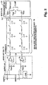
- FIGS 2 and 3 illustrate a further embodiment of the invention as an optimization to signal readout.
- the sense amp cell 116 in this embodiment includes a pair of operational amplifiers (opamps) A 1 and A 2 configured as unity-gain closed loop amplifiers.
- the amplifiers drive their respective input signals (voltages on capacitors C SA1 and C SA2 obtained by sampling the output line) through the analog mux 118 which is represented as several pairs of switches or gates that may include parasitic resistances (R) and capacitances (C).
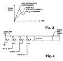
- At least one and preferably both of the opamps is configured to yield an underdamped response at its output node (node "INTERMEDIATE") as shown in Figure 3 when driving a signal through its load, the load being the signal path through analog multiplexer 118 and, optionally, into the differencing unit 122.
- the pair of opamps are configured to yield a critically damped response at the near plates of the capacitors C DU1 and C DU2 (node "OUT”) in the optional differencing unit. Designing the opamp to give a critically damped response at the end of the signal path through the mux 118 rather than at its output node reduces the settling time of the signal at node OUT.
- the settling time may be defined in the context of a circuit's transient response as the time interval between the stimulus (activating the sense amp cell and creating a path through the analog mux) and its response (one or both of the differential signal pair settling to less than, for example, 0.1% of their steady state value).
- a faster settling time for each differential signal pair in turn allows the entire storage array 110 to be read significantly more quickly, as the slightest reduction in settling time of the differential signal pair is multiplied by a very large number of cells in the storage array, e.g., 1 million for a 1024 ⁇ 1024 image sensor array, to give a significant speed advantage during readout of the entire array 110.
- DDS normally operates in a two phase manner.
- the cell 116 drives the exposed and reset values while the CLAMP signal is asserted in the DDS unit 122 and predetermined common mode voltage V CM1 is applied to the far plates (see Figure 2 ).
- CROWBAR CB
- CLAMP is deasserted.
- DDS causes an average of the exposed and reset values to be driven by the cell 116 into the DDS unit.
- CLAMP and CB results in the reduction of errors caused by offsets in opamps A 1 and A 2 , albeit requiring an additional readout cycle for each pixel.
- Figures 4-6 show circuits and a related timing diagram that can be used to reduce power consumption in systems having large analog storage arrays 110 (see Figure 1 ).
- This embodiment also yields a scalable readout architecture in which the increase in power consumption by going to a larger array is significantly less than in an architecture in which the entire sense amplifier array 114 is kept energized while the signals are driven into the analog mux 118 (see Figure 1 ).
- the sense amp array 114 and timing signals are configured such that all but two of the sense amp cells at any given moment are kept inactive in order to reduce power consumption.
- the inactive state of each cell is defined as the state in which the cell consumes the least power while still being able to maintain the sampled signal pair values on the capacitors C SA1 and C SA2 until the values are read.
- the opamps A 1 and A 2 in each cell feature an enable input that permits the opamp to be switched to a low power mode or even shut off in the inactive state.
- the array 114 is read by sequentially activating a pair of adjacent sense amp cells.
- the sense amp cells can be configured as shown in Figure 5.
- a switch pair 520 is provided in series with the amplifier output nodes, where the switch pair is controlled by the Select signal.
- An OR gate 524 receives the Select and Select_Ahead signals and controls the Enable input of the amplifiers.
- the Select and a Select_Ahead signal come from a timing signal generation circuit 708 (see Figure 7 ).
- An exemplary timing diagram showing the Select and Select_Ahead signals as pulses is shown in Figure 6 as referenced to a master clock and will be explained by the following example.
- the near cell (cell 0 of the 0/1 pair) is active and its opamps are driving a differential signal pair into the analog mux.
- the far cell (cell 1 of the 0/1 pair) is active, but no signals are being driven from that cell, because its Select input is deasserted as shown by pulse 1 /2.
- pulse 0/1 is deasserted (which deactivates cell 0) and pulse 1/2 is asserted to activate a subsequent pair of sense amp cells.
- the latter event both maintains cell 1 in the active state and activates cell 2.
- a new differential signal pair is thus driven only by cell 1.
- the embodiments of the invention described above can be incorporated into an imaging apparatus 700 shown in logical block diagram form in Figure 7 .
- the apparatus 700 includes an image sensor array 710 that is part of an analog signal readout architecture that incorporates one or more of the embodiments illustrated in Figures 1-6 and described above.
- An optical system 706 having a lens and aperture is adjusted to project an image of an object onto a focal plane that contains the image sensor array 710.
- the image sensor array 710 provides a number of bit lines, one for each column of the array, that are used to transfer pixel signals to a correlated double sampling (CDS) array 714.
- CDS array provides a differential signal pair for each column of the sensor array 710 and is used to readout the pixel signals one row at a time.
- the differential signal pairs for a row of the sensor array are then fed to an analog multiplexer 118.
- the analog multiplexer may have the configuration illustrated in Figure 1 and described above.
- the technique of using a Select and a Select_Ahead signal to energize only a pair of adjacent CDS cells at a time can be used to further enhance the performance of the apparatus 700.
- the differential signal pairs are then sequentially fed to a double difference sampling (DDS) unit 722 where further noise reduction takes place.
- DDS double difference sampling
- the differential signal pair may then be transferred to an analog-to-digital converter unit 726 to be converted into digital format.
- digital signal and image processing (DSIP) 730 is performed on the digital signals to obtain image data having a desired resolution.
- the DSIP 730 may include hardwired logic circuitry or a programmed high performance processor that performs color correction, scaling, and compression if desired to further reduce the size of the image data.
- the compressed image data may be transferred to a host computer through a communication interface that operates according to any one of known computer peripheral bus standards, such as Universal Serial Bus (USB) and IEEE 1394-1995.
- the apparatus 700 may optionally include a local storage device such as a removable memory card for nonvolatile storage of the image data.
- the overall operation of apparatus 700 may be managed by a system controller 712 that provides control and data signals to a timing signal and column address generation unit 708 as well as the DSIP unit 730.
- the system controller 712 may include a microcontroller, or a processor having an input/output interface, that responds to instructions stored in a nonvolatile memory, e.g., firmware (not shown), in the system controller.
- the various timing signals Select and Select_Ahead used by the CDS array 714 and column addresses used by the analog multiplexer can be generated by hardwired logic circuitry within the timing signal and address generation unit 708.
- the system controller 712 may be enhanced to provide the timing signal and address generation functions itself.
Landscapes
- Engineering & Computer Science (AREA)
- Multimedia (AREA)
- Signal Processing (AREA)
- Transforming Light Signals Into Electric Signals (AREA)
Applications Claiming Priority (3)
| Application Number | Priority Date | Filing Date | Title |
|---|---|---|---|
| US987131 | 1992-12-07 | ||
| US08/987,131 US6366320B1 (en) | 1997-12-08 | 1997-12-08 | High speed readout architecture for analog storage arrays |
| PCT/US1998/023872 WO1999030484A1 (en) | 1997-12-08 | 1998-11-09 | High speed readout architecture for analog storage arrays |
Publications (3)
| Publication Number | Publication Date |
|---|---|
| EP1038390A1 EP1038390A1 (en) | 2000-09-27 |
| EP1038390A4 EP1038390A4 (en) | 2001-02-28 |
| EP1038390B1 true EP1038390B1 (en) | 2004-10-13 |
Family
ID=25533061
Family Applications (1)
| Application Number | Title | Priority Date | Filing Date |
|---|---|---|---|
| EP98958504A Expired - Lifetime EP1038390B1 (en) | 1997-12-08 | 1998-11-09 | High speed readout architecture for analog storage arrays |
Country Status (8)
| Country | Link |
|---|---|
| US (1) | US6366320B1 (https=) |
| EP (1) | EP1038390B1 (https=) |
| JP (1) | JP4444499B2 (https=) |
| KR (1) | KR100403290B1 (https=) |
| AU (1) | AU1453599A (https=) |
| DE (1) | DE69827034T2 (https=) |
| TW (1) | TW398136B (https=) |
| WO (1) | WO1999030484A1 (https=) |
Families Citing this family (22)
| Publication number | Priority date | Publication date | Assignee | Title |
|---|---|---|---|---|
| US6847399B1 (en) * | 1998-03-23 | 2005-01-25 | Micron Technology, Inc. | Increasing readout speed in CMOS APS sensors through block readout |
| US7674293B2 (en) * | 2004-04-22 | 2010-03-09 | Facet Solutions, Inc. | Crossbar spinal prosthesis having a modular design and related implantation methods |
| US6463566B1 (en) * | 2000-02-04 | 2002-10-08 | Massachusetts Institute Of Technology | Dynamic double sampling charge integrator |
| US7154548B2 (en) * | 2001-01-29 | 2006-12-26 | Valley Oak Semiconductor | Multiplexed and pipelined column buffer for use with an array of photo sensors |
| US7088394B2 (en) * | 2001-07-09 | 2006-08-08 | Micron Technology, Inc. | Charge mode active pixel sensor read-out circuit |
| US6982758B2 (en) * | 2001-07-23 | 2006-01-03 | Micron Technology, Inc. | Flexy-power amplifier: a new amplifier with built-in power management |
| US6838787B2 (en) * | 2002-01-16 | 2005-01-04 | Eastman Kodak Company | Variable bandwidth correlated doubling sampling circuits for image sensors |
| US7068319B2 (en) * | 2002-02-01 | 2006-06-27 | Micron Technology, Inc. | CMOS image sensor with a low-power architecture |
| EP1429542A1 (en) * | 2002-12-11 | 2004-06-16 | Dialog Semiconductor GmbH | Fixed pattern noise compensation with low memory requirements |
| US6953923B2 (en) * | 2003-02-18 | 2005-10-11 | Omnivision Technologies, Inc. | CMOS image sensor having reduced numbers of column readout circuits |
| US7821555B2 (en) * | 2003-04-21 | 2010-10-26 | Micron Technology, Inc. | Multi path power for CMOS imagers |
| US20040246354A1 (en) * | 2003-06-04 | 2004-12-09 | Hongli Yang | CMOS image sensor having high speed sub sampling |
| KR100656666B1 (ko) * | 2004-09-08 | 2006-12-11 | 매그나칩 반도체 유한회사 | 이미지 센서 |
| US20060170788A1 (en) * | 2005-02-03 | 2006-08-03 | Transchip, Inc. | Image sensor with balanced switching noise |
| US7545834B1 (en) | 2006-01-10 | 2009-06-09 | Pericom Semiconductor Corp. | Multiple channel switch using differential de-mux amplifier and differential mux equalizer |
| US7342212B2 (en) * | 2006-03-31 | 2008-03-11 | Micron Technology, Inc. | Analog vertical sub-sampling in an active pixel sensor (APS) image sensor |
| US20070285547A1 (en) * | 2006-05-30 | 2007-12-13 | Milligan Edward S | CMOS image sensor array optimization for both bright and low light conditions |
| JP4458113B2 (ja) * | 2007-05-02 | 2010-04-28 | ソニー株式会社 | データ転送回路、固体撮像素子、およびカメラシステム |
| US20090091648A1 (en) * | 2007-10-09 | 2009-04-09 | Shengmin Lin | Multi-resolution Image Sensor Array with High Image Quality Pixel Readout Circuitry |
| US20110286271A1 (en) * | 2010-05-21 | 2011-11-24 | Mediatek Inc. | Memory systems and methods for reading data stored in a memory cell of a memory device |
| US9191582B1 (en) * | 2011-04-29 | 2015-11-17 | Bae Systems Information And Electronic Systems Integration Inc. | Multi-mode high speed sensor |
| KR102410898B1 (ko) * | 2021-02-23 | 2022-06-22 | 광주과학기술원 | 전류 모드 라인 드라이버 장치 및 이의 동작 방법 |
Family Cites Families (8)
| Publication number | Priority date | Publication date | Assignee | Title |
|---|---|---|---|---|
| US4237383A (en) * | 1978-09-20 | 1980-12-02 | Rca Corporation | High speed loading of output register of CCD array system |
| US4322752A (en) * | 1980-01-16 | 1982-03-30 | Eastman Technology, Inc. | Fast frame rate sensor readout |
| US4734583A (en) * | 1986-10-16 | 1988-03-29 | General Electric Company | Readout circuit for dual-gate CID imagers with charge sharing corrected for subtractive error |
| US4862276A (en) * | 1988-10-07 | 1989-08-29 | Wang Samuel C | Push-pull readout of dual gate cid arrays |
| US5351309A (en) * | 1992-06-30 | 1994-09-27 | National Science Council | Image edge sensor |
| US5471515A (en) | 1994-01-28 | 1995-11-28 | California Institute Of Technology | Active pixel sensor with intra-pixel charge transfer |
| US5736886A (en) * | 1996-02-06 | 1998-04-07 | Analog Devices, Inc. | Input clamping method and apparatus with a correlated double-sampling circuit |
| US5877715A (en) * | 1997-06-12 | 1999-03-02 | International Business Machines Corporation | Correlated double sampling with up/down counter |
-
1997
- 1997-12-08 US US08/987,131 patent/US6366320B1/en not_active Expired - Lifetime
-
1998
- 1998-11-09 JP JP2000524917A patent/JP4444499B2/ja not_active Expired - Fee Related
- 1998-11-09 DE DE69827034T patent/DE69827034T2/de not_active Expired - Lifetime
- 1998-11-09 EP EP98958504A patent/EP1038390B1/en not_active Expired - Lifetime
- 1998-11-09 AU AU14535/99A patent/AU1453599A/en not_active Abandoned
- 1998-11-09 WO PCT/US1998/023872 patent/WO1999030484A1/en not_active Ceased
- 1998-11-09 KR KR10-2000-7006125A patent/KR100403290B1/ko not_active Expired - Fee Related
- 1998-12-07 TW TW087120266A patent/TW398136B/zh not_active IP Right Cessation
Also Published As
| Publication number | Publication date |
|---|---|
| AU1453599A (en) | 1999-06-28 |
| TW398136B (en) | 2000-07-11 |
| DE69827034T2 (de) | 2005-09-08 |
| US6366320B1 (en) | 2002-04-02 |
| JP2001526498A (ja) | 2001-12-18 |
| KR100403290B1 (ko) | 2003-10-30 |
| DE69827034D1 (de) | 2004-11-18 |
| EP1038390A4 (en) | 2001-02-28 |
| JP4444499B2 (ja) | 2010-03-31 |
| KR20010032808A (ko) | 2001-04-25 |
| EP1038390A1 (en) | 2000-09-27 |
| WO1999030484A1 (en) | 1999-06-17 |
Similar Documents
| Publication | Publication Date | Title |
|---|---|---|
| EP1038390B1 (en) | High speed readout architecture for analog storage arrays | |
| CN108574809B (zh) | 像素、像素驱动电路以及包括其的视觉传感器 | |
| JP3868648B2 (ja) | イメージセンサ装置及び半導体イメージセンシング装置 | |
| US7898588B2 (en) | Dual conversion gain gate and capacitor and HDR combination | |
| JP4362156B2 (ja) | Cmos領域アレイ・センサのための逐次相関ダブル・サンプリング方式 | |
| JP3408045B2 (ja) | 光電変換装置 | |
| US20120161214A1 (en) | Cmos image sensor with shared sensing mode | |
| JPH11266404A (ja) | Cmos領域アレイ・センサのための不整合非依存リセット感知 | |
| US10230915B2 (en) | Image capturing apparatus and image capturing system | |
| US6710803B1 (en) | Image sensor and method for driving the same | |
| JP2009089069A (ja) | 画素駆動回路および撮像装置ならびにカメラシステム | |
| EP3808072B1 (en) | Image sensor | |
| US10965890B2 (en) | Imaging device and imaging system | |
| US6346696B1 (en) | Image sensor and method for driving the same | |
| JP2001203936A (ja) | 画像記録装置 | |
| US6697108B1 (en) | Fast frame readout architecture for array sensors with integrated correlated double sampling system | |
| US9040894B2 (en) | Imager with column readout | |
| US11258966B2 (en) | Photoelectric conversion device, camera, movable object, and signal processing device | |
| Vogelsong et al. | Scientific/industrial camera-on-a-chip using active column sensor CMOS imager core | |
| EP0928102B1 (en) | Array sensors | |
| JP2008300931A (ja) | 撮像装置 | |
| JP2008160438A (ja) | 固体撮像装置 | |
| TWI897296B (zh) | 像素排列、成像裝置及用於操作像素排列之方法 | |
| WO2023080180A1 (ja) | 撮像素子および撮像装置 | |
| JP2026063198A (ja) | 撮像素子および撮像装置 |
Legal Events
| Date | Code | Title | Description |
|---|---|---|---|
| PUAI | Public reference made under article 153(3) epc to a published international application that has entered the european phase |
Free format text: ORIGINAL CODE: 0009012 |
|
| 17P | Request for examination filed |
Effective date: 20000613 |
|
| AK | Designated contracting states |
Kind code of ref document: A1 Designated state(s): DE GB NL |
|
| A4 | Supplementary search report drawn up and despatched |
Effective date: 20010115 |
|
| AK | Designated contracting states |
Kind code of ref document: A4 Designated state(s): DE GB NL |
|
| RIC1 | Information provided on ipc code assigned before grant |
Free format text: 7H 04N 3/14 A, 7H 04N 5/335 B, 7G 11C 27/00 B |
|
| 17Q | First examination report despatched |
Effective date: 20031022 |
|
| GRAP | Despatch of communication of intention to grant a patent |
Free format text: ORIGINAL CODE: EPIDOSNIGR1 |
|
| GRAS | Grant fee paid |
Free format text: ORIGINAL CODE: EPIDOSNIGR3 |
|
| GRAA | (expected) grant |
Free format text: ORIGINAL CODE: 0009210 |
|
| AK | Designated contracting states |
Kind code of ref document: B1 Designated state(s): DE GB NL |
|
| REG | Reference to a national code |
Ref country code: GB Ref legal event code: FG4D |
|
| REF | Corresponds to: |
Ref document number: 69827034 Country of ref document: DE Date of ref document: 20041118 Kind code of ref document: P |
|
| PLBE | No opposition filed within time limit |
Free format text: ORIGINAL CODE: 0009261 |
|
| STAA | Information on the status of an ep patent application or granted ep patent |
Free format text: STATUS: NO OPPOSITION FILED WITHIN TIME LIMIT |
|
| 26N | No opposition filed |
Effective date: 20050714 |
|
| PGFP | Annual fee paid to national office [announced via postgrant information from national office to epo] |
Ref country code: DE Payment date: 20091127 Year of fee payment: 12 |
|
| PGFP | Annual fee paid to national office [announced via postgrant information from national office to epo] |
Ref country code: NL Payment date: 20091123 Year of fee payment: 12 |
|
| PGFP | Annual fee paid to national office [announced via postgrant information from national office to epo] |
Ref country code: GB Payment date: 20091125 Year of fee payment: 12 |
|
| REG | Reference to a national code |
Ref country code: NL Ref legal event code: V1 Effective date: 20110601 |
|
| GBPC | Gb: european patent ceased through non-payment of renewal fee |
Effective date: 20101109 |
|
| PG25 | Lapsed in a contracting state [announced via postgrant information from national office to epo] |
Ref country code: NL Free format text: LAPSE BECAUSE OF NON-PAYMENT OF DUE FEES Effective date: 20110601 |
|
| REG | Reference to a national code |
Ref country code: DE Ref legal event code: R119 Ref document number: 69827034 Country of ref document: DE Effective date: 20110601 Ref country code: DE Ref legal event code: R119 Ref document number: 69827034 Country of ref document: DE Effective date: 20110531 |
|
| PG25 | Lapsed in a contracting state [announced via postgrant information from national office to epo] |
Ref country code: DE Free format text: LAPSE BECAUSE OF NON-PAYMENT OF DUE FEES Effective date: 20110531 |
|
| PG25 | Lapsed in a contracting state [announced via postgrant information from national office to epo] |
Ref country code: GB Free format text: LAPSE BECAUSE OF NON-PAYMENT OF DUE FEES Effective date: 20101109 |