EP1037261A2 - Etching and cleaning methods and etching and cleaning apparatuses used therefor - Google Patents
Etching and cleaning methods and etching and cleaning apparatuses used therefor Download PDFInfo
- Publication number
- EP1037261A2 EP1037261A2 EP00104585A EP00104585A EP1037261A2 EP 1037261 A2 EP1037261 A2 EP 1037261A2 EP 00104585 A EP00104585 A EP 00104585A EP 00104585 A EP00104585 A EP 00104585A EP 1037261 A2 EP1037261 A2 EP 1037261A2
- Authority
- EP
- European Patent Office
- Prior art keywords
- wafer
- nozzle
- etching
- emitted
- liquid
- Prior art date
- Legal status (The legal status is an assumption and is not a legal conclusion. Google has not performed a legal analysis and makes no representation as to the accuracy of the status listed.)
- Granted
Links
Images






Classifications
-
- C—CHEMISTRY; METALLURGY
- C23—COATING METALLIC MATERIAL; COATING MATERIAL WITH METALLIC MATERIAL; CHEMICAL SURFACE TREATMENT; DIFFUSION TREATMENT OF METALLIC MATERIAL; COATING BY VACUUM EVAPORATION, BY SPUTTERING, BY ION IMPLANTATION OR BY CHEMICAL VAPOUR DEPOSITION, IN GENERAL; INHIBITING CORROSION OF METALLIC MATERIAL OR INCRUSTATION IN GENERAL
- C23F—NON-MECHANICAL REMOVAL OF METALLIC MATERIAL FROM SURFACE; INHIBITING CORROSION OF METALLIC MATERIAL OR INCRUSTATION IN GENERAL; MULTI-STEP PROCESSES FOR SURFACE TREATMENT OF METALLIC MATERIAL INVOLVING AT LEAST ONE PROCESS PROVIDED FOR IN CLASS C23 AND AT LEAST ONE PROCESS COVERED BY SUBCLASS C21D OR C22F OR CLASS C25
- C23F1/00—Etching metallic material by chemical means
- C23F1/10—Etching compositions
- C23F1/14—Aqueous compositions
- C23F1/16—Acidic compositions
- C23F1/26—Acidic compositions for etching refractory metals
-
- B—PERFORMING OPERATIONS; TRANSPORTING
- B08—CLEANING
- B08B—CLEANING IN GENERAL; PREVENTION OF FOULING IN GENERAL
- B08B3/00—Cleaning by methods involving the use or presence of liquid or steam
- B08B3/02—Cleaning by the force of jets or sprays
-
- C—CHEMISTRY; METALLURGY
- C23—COATING METALLIC MATERIAL; COATING MATERIAL WITH METALLIC MATERIAL; CHEMICAL SURFACE TREATMENT; DIFFUSION TREATMENT OF METALLIC MATERIAL; COATING BY VACUUM EVAPORATION, BY SPUTTERING, BY ION IMPLANTATION OR BY CHEMICAL VAPOUR DEPOSITION, IN GENERAL; INHIBITING CORROSION OF METALLIC MATERIAL OR INCRUSTATION IN GENERAL
- C23F—NON-MECHANICAL REMOVAL OF METALLIC MATERIAL FROM SURFACE; INHIBITING CORROSION OF METALLIC MATERIAL OR INCRUSTATION IN GENERAL; MULTI-STEP PROCESSES FOR SURFACE TREATMENT OF METALLIC MATERIAL INVOLVING AT LEAST ONE PROCESS PROVIDED FOR IN CLASS C23 AND AT LEAST ONE PROCESS COVERED BY SUBCLASS C21D OR C22F OR CLASS C25
- C23F1/00—Etching metallic material by chemical means
- C23F1/08—Apparatus, e.g. for photomechanical printing surfaces
-
- C—CHEMISTRY; METALLURGY
- C23—COATING METALLIC MATERIAL; COATING MATERIAL WITH METALLIC MATERIAL; CHEMICAL SURFACE TREATMENT; DIFFUSION TREATMENT OF METALLIC MATERIAL; COATING BY VACUUM EVAPORATION, BY SPUTTERING, BY ION IMPLANTATION OR BY CHEMICAL VAPOUR DEPOSITION, IN GENERAL; INHIBITING CORROSION OF METALLIC MATERIAL OR INCRUSTATION IN GENERAL
- C23F—NON-MECHANICAL REMOVAL OF METALLIC MATERIAL FROM SURFACE; INHIBITING CORROSION OF METALLIC MATERIAL OR INCRUSTATION IN GENERAL; MULTI-STEP PROCESSES FOR SURFACE TREATMENT OF METALLIC MATERIAL INVOLVING AT LEAST ONE PROCESS PROVIDED FOR IN CLASS C23 AND AT LEAST ONE PROCESS COVERED BY SUBCLASS C21D OR C22F OR CLASS C25
- C23F1/00—Etching metallic material by chemical means
- C23F1/10—Etching compositions
- C23F1/14—Aqueous compositions
- C23F1/16—Acidic compositions
- C23F1/18—Acidic compositions for etching copper or alloys thereof
-
- C—CHEMISTRY; METALLURGY
- C23—COATING METALLIC MATERIAL; COATING MATERIAL WITH METALLIC MATERIAL; CHEMICAL SURFACE TREATMENT; DIFFUSION TREATMENT OF METALLIC MATERIAL; COATING BY VACUUM EVAPORATION, BY SPUTTERING, BY ION IMPLANTATION OR BY CHEMICAL VAPOUR DEPOSITION, IN GENERAL; INHIBITING CORROSION OF METALLIC MATERIAL OR INCRUSTATION IN GENERAL
- C23G—CLEANING OR DE-GREASING OF METALLIC MATERIAL BY CHEMICAL METHODS OTHER THAN ELECTROLYSIS
- C23G3/00—Apparatus for cleaning or pickling metallic material
-
- H—ELECTRICITY
- H10—SEMICONDUCTOR DEVICES; ELECTRIC SOLID-STATE DEVICES NOT OTHERWISE PROVIDED FOR
- H10P—GENERIC PROCESSES OR APPARATUS FOR THE MANUFACTURE OR TREATMENT OF DEVICES COVERED BY CLASS H10
- H10P50/00—Etching of wafers, substrates or parts of devices
- H10P50/60—Wet etching
- H10P50/64—Wet etching of semiconductor materials
- H10P50/642—Chemical etching
-
- H—ELECTRICITY
- H10—SEMICONDUCTOR DEVICES; ELECTRIC SOLID-STATE DEVICES NOT OTHERWISE PROVIDED FOR
- H10P—GENERIC PROCESSES OR APPARATUS FOR THE MANUFACTURE OR TREATMENT OF DEVICES COVERED BY CLASS H10
- H10P50/00—Etching of wafers, substrates or parts of devices
- H10P50/60—Wet etching
- H10P50/66—Wet etching of conductive or resistive materials
- H10P50/663—Wet etching of conductive or resistive materials by chemical means only
- H10P50/667—Wet etching of conductive or resistive materials by chemical means only by liquid etching only
-
- H—ELECTRICITY
- H10—SEMICONDUCTOR DEVICES; ELECTRIC SOLID-STATE DEVICES NOT OTHERWISE PROVIDED FOR
- H10P—GENERIC PROCESSES OR APPARATUS FOR THE MANUFACTURE OR TREATMENT OF DEVICES COVERED BY CLASS H10
- H10P70/00—Cleaning of wafers, substrates or parts of devices
- H10P70/20—Cleaning during device manufacture
- H10P70/23—Cleaning during device manufacture during, before or after processing of insulating materials
- H10P70/234—Cleaning during device manufacture during, before or after processing of insulating materials the processing being the formation of vias or contact holes
-
- H—ELECTRICITY
- H10—SEMICONDUCTOR DEVICES; ELECTRIC SOLID-STATE DEVICES NOT OTHERWISE PROVIDED FOR
- H10P—GENERIC PROCESSES OR APPARATUS FOR THE MANUFACTURE OR TREATMENT OF DEVICES COVERED BY CLASS H10
- H10P70/00—Cleaning of wafers, substrates or parts of devices
- H10P70/20—Cleaning during device manufacture
- H10P70/27—Cleaning during device manufacture during, before or after processing of conductive materials, e.g. polysilicon or amorphous silicon layers
- H10P70/277—Cleaning during device manufacture during, before or after processing of conductive materials, e.g. polysilicon or amorphous silicon layers the processing being a planarisation of conductive layers
-
- H—ELECTRICITY
- H10—SEMICONDUCTOR DEVICES; ELECTRIC SOLID-STATE DEVICES NOT OTHERWISE PROVIDED FOR
- H10P—GENERIC PROCESSES OR APPARATUS FOR THE MANUFACTURE OR TREATMENT OF DEVICES COVERED BY CLASS H10
- H10P70/00—Cleaning of wafers, substrates or parts of devices
- H10P70/50—Cleaning of wafers, substrates or parts of devices characterised by the part to be cleaned
- H10P70/54—Cleaning of wafer edges
-
- H—ELECTRICITY
- H10—SEMICONDUCTOR DEVICES; ELECTRIC SOLID-STATE DEVICES NOT OTHERWISE PROVIDED FOR
- H10P—GENERIC PROCESSES OR APPARATUS FOR THE MANUFACTURE OR TREATMENT OF DEVICES COVERED BY CLASS H10
- H10P70/00—Cleaning of wafers, substrates or parts of devices
- H10P70/50—Cleaning of wafers, substrates or parts of devices characterised by the part to be cleaned
- H10P70/56—Cleaning of wafer backside
-
- H—ELECTRICITY
- H10—SEMICONDUCTOR DEVICES; ELECTRIC SOLID-STATE DEVICES NOT OTHERWISE PROVIDED FOR
- H10P—GENERIC PROCESSES OR APPARATUS FOR THE MANUFACTURE OR TREATMENT OF DEVICES COVERED BY CLASS H10
- H10P72/00—Handling or holding of wafers, substrates or devices during manufacture or treatment thereof
- H10P72/04—Apparatus for manufacture or treatment
- H10P72/0402—Apparatus for fluid treatment
- H10P72/0404—Apparatus for fluid treatment for general liquid treatment, e.g. etching followed by cleaning
-
- H—ELECTRICITY
- H10—SEMICONDUCTOR DEVICES; ELECTRIC SOLID-STATE DEVICES NOT OTHERWISE PROVIDED FOR
- H10P—GENERIC PROCESSES OR APPARATUS FOR THE MANUFACTURE OR TREATMENT OF DEVICES COVERED BY CLASS H10
- H10P72/00—Handling or holding of wafers, substrates or devices during manufacture or treatment thereof
- H10P72/04—Apparatus for manufacture or treatment
- H10P72/0402—Apparatus for fluid treatment
- H10P72/0406—Apparatus for fluid treatment for cleaning followed by drying, rinsing, stripping, blasting or the like
- H10P72/0411—Apparatus for fluid treatment for cleaning followed by drying, rinsing, stripping, blasting or the like for wet cleaning or washing
- H10P72/0414—Apparatus for fluid treatment for cleaning followed by drying, rinsing, stripping, blasting or the like for wet cleaning or washing using mainly spraying means, e.g. nozzles
-
- H—ELECTRICITY
- H10—SEMICONDUCTOR DEVICES; ELECTRIC SOLID-STATE DEVICES NOT OTHERWISE PROVIDED FOR
- H10P—GENERIC PROCESSES OR APPARATUS FOR THE MANUFACTURE OR TREATMENT OF DEVICES COVERED BY CLASS H10
- H10P72/00—Handling or holding of wafers, substrates or devices during manufacture or treatment thereof
- H10P72/04—Apparatus for manufacture or treatment
- H10P72/0402—Apparatus for fluid treatment
- H10P72/0418—Apparatus for fluid treatment for etching
- H10P72/0422—Apparatus for fluid treatment for etching for wet etching
- H10P72/0424—Apparatus for fluid treatment for etching for wet etching using mainly spraying means, e.g. nozzles
-
- H—ELECTRICITY
- H10—SEMICONDUCTOR DEVICES; ELECTRIC SOLID-STATE DEVICES NOT OTHERWISE PROVIDED FOR
- H10P—GENERIC PROCESSES OR APPARATUS FOR THE MANUFACTURE OR TREATMENT OF DEVICES COVERED BY CLASS H10
- H10P72/00—Handling or holding of wafers, substrates or devices during manufacture or treatment thereof
- H10P72/70—Handling or holding of wafers, substrates or devices during manufacture or treatment thereof for supporting or gripping
- H10P72/76—Handling or holding of wafers, substrates or devices during manufacture or treatment thereof for supporting or gripping using mechanical means, e.g. clamps or pinches
- H10P72/7602—Handling or holding of wafers, substrates or devices during manufacture or treatment thereof for supporting or gripping using mechanical means, e.g. clamps or pinches the wafers being placed on a robot blade or gripped by a gripper for conveyance
Definitions
- the present invention relates to etching and cleaning methods and etching and cleaning apparatuses used for semiconductor device fabrication and more particularly, to etching and cleaning methods of removing an unnecessary or undesired material or materials from a semiconductor wafer and etching and cleaning apparatuses used for performing the etching or cleaning method.
- the "end face” means the end face of the wafer located between its surface and back and approximately perpendicular to them.
- the "surface peripheral area” means the area or region of the surface of the wafer between the device area and the end face.
- the device area is an area or region of the surface of the wafer in which desired semiconductor devices are formed.
- the "back peripheral area” means the area or region of the back of the wafer in which an undesired or unnecessary material or materials to be removed are present.
- Cu wiring lines are typically formed in trenches of a silicon dioxide (SiO 2 ) film, which are usually realized by the step of forming the trenches in the SiO 2 film, the step of forming a Cu film on the SiO 2 film to cover the trenches by electroplating, and the step of selectively removing the Cu film to leave the same in the trenches by Chemical Mechanical Polishing (CMP).
- CMP Chemical Mechanical Polishing
- trenches are formed in a SiO 2 film to have a pattern for desired wiring lines by a known method, where the SiO 2 film is formed on or over a single-crystal silicon (Si) wafer or substrate.
- a barrier metal film which is made of meal such as tantalum (Ta) and tantalum nitride (TaN), is formed on the SiO 2 film to cover the trenches by sputtering. The barrier metal film is to prevent the Cu atoms from diffusing into the SiO 2 film.
- a seed Cu film is formed on the barrier metal film by sputtering.
- a wiring Cu film is formed on the seed Cu film by electroplating.
- a ring-shaped blocking member is placed on the surface of the wafer to surround the device area and then, a proper plating liquid or solution is supplied to the inside of the member. At this time, there is a possibility that the plating liquid leaks out of the member. If leakage of the liquid occurs, the wiring Cu film is formed not only in the device area but also in the surface peripheral area of the wafer. The wiring Cu film thus formed in the surface peripheral area is unnecessary and to be removed. The unnecessary Cu film tends to be detached from the SiO 2 film in the subsequent process or processes due to stress to thereby contaminate the production lines of the semiconductor device, because of weak adhesion of the plated Cu film to the SiO 2 film. As a result, the unnecessary Cu film needs to be removed.
- the Si wafer is contaminated by Cu wastes produced from the Cu film polished.
- the Cu wastes tend to diffuse into the SiO 2 film and the Si wafer due to subsequent heat treatment, thereby badly affecting the performance of the semiconductor devices formed in the device area. Since the Cu wastes adhere onto the surface and back peripheral areas and the end face of the wafer, they are difficult to be removed therefrom. Thus, the Cu wastes need to be removed by cleaning.
- the distance between the edge of the device area and the end face of the wafer is typically set as, for example, approximately 5 mm.
- the SiO 2 film in which the Cu wiring lines are formed
- the SiO 2 film is formed on the wafer to be expanded until the distance between the edge of the SiO 2 film and the end face is decreased to 1.5 mm to 2.0 mm.
- the seed Cu film is deposited onto the barrier metal film over the whole wafer by sputtering in order to cover the whole SiO 2 film, it tends to cover not only the device area but also the surface and back peripheral areas and the end face of the wafer.
- the wiring Cu film tends to be formed on the seed film not only in the device area but also in the surface and back peripheral areas and the end face.
- the wiring Cu film is formed on the seed Cu film, it is not separated or stripped off.
- the wiring Cu film existing on the end face of the wafer tends to be adhered onto the wafer carriers and/or the robot arms during transportation processes in the semiconductor device fabrication system. Thus, it tends to contaminate the transportation subsystem. This means that the wiring Cu film existing on the surface and back peripheral areas and the end face of the wafer needs to be removed before the wafer is transported to the next stage.
- the removal of the above-described wiring Cu film requires good controllability. This is because the distance between the edge of the SiO 2 film and the end face is as short as 1.5 mm to 2 mm.
- the cleaning of the above-described Cu contaminants generated in the CMP process also necessitates similar good controllability.
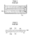
- a protection film 112 having an etch-resistant property is selectively formed on the surface 110A of a semiconductor wafer 110 to cover the entire device area formed thereon. Then, the wafer 110 with the film 112 is entirely immersed into an etching solution 114 stored in a suitable container 113, thereby etching selectively the exposed area of the wafer 110. Thus, the exposed area is cleaned. Thereafter, the film 112 is removed from the wafer 110.
- etching solution 114 for example, a mixture of hydrogen fluoride (HF), hydrogen peroxide (H 2 O 2 ), and water (H 2 O), which is often termed “Fluoric-Peroxide Mixture (FPM)", may be used.
- HF hydrogen fluoride
- H 2 O 2 hydrogen peroxide
- H 2 O water
- FPM Fluoric-Peroxide Mixture
- a semiconductor wafer 110 is rotated in a horizontal plane by a proper rotating means while it is turned upside down.
- an etching solution 114 e.g., FPM
- a protection gas 115 e.g., nitrogen gas, N 2
- N 2 nitrogen gas
- the solution 114 thus supplied onto the back 110B moves outward to the end face 110C of the wafer 110 along the back 110B and then, flows along the vertical end face 110C, and drops from the end face 110C. Part of the solution 114 reaches the periphery of the surface 110A and then, it is dropped therefrom.
- the protection gas 115 thus supplied to the surface 110A keeps the device area not to be contacted with the etching solution 114.
- the solution 114 selectively etches the back 110B, the end face 110C, and the periphery of the surface 110A, thereby cleaning them.
- the flow of the etching solution 114 toward the back 110B of the wafer 110 is controlled by the rotation speed of the wafer 110 and the flow rate of the protection gas 115 toward the surface 110A.
- the controllability is low.
- the circular edge of the flowing solution 114 which is defined by contact or collision of the solution 114 with the gas 115 and extends along the edge of the wafer 110, tends to wave or fluctuate.
- the solution 114 may reach the device area at some location to etch the same. Alternately, the solution 114 does not contact with the periphery of the surface 110A at some location, leaving the undesired material thereon.
- the prior-art cleaning/etching method shown in Fig. 2 is unable to be applied to the case where the distance between the edge of the device area and the end face of the wafer is as short as 1.5 mm to 2.0 mm.
- an object of the present invention is to provide an etching method and an etching apparatus that make it possible to effectively remove an unnecessary material or materials existing on a semiconductor wafer without damaging the device area.
- Another object of the present invention is to provide an etching method and an etching apparatus that make it possible to effectively remove an unnecessary material or materials existing on a semiconductor wafer with good controllability.
- Still another object of the present invention is to provide an etching method and an etching apparatus that removes effectively an unnecessary material or materials existing on a semiconductor wafer even if the distance between the edge of the device area and the end face of the wafer is as short as approximately 1.5 mm to 2.0 mm.
- a further object of the present invention is to provide a cleaning method and a cleaning apparatus that make it possible to effectively clean a semiconductor wafer without damaging the device area.
- a still further object of the present invention is to provide a cleaning method and a cleaning apparatus that make it possible to effectively clean a semiconductor wafer with good controllability.
- a still further object of the present invention is to provide a cleaning method and a cleaning apparatus that cleans effectively a semiconductor wafer even if the distance between the edge of the device area and the end face of the wafer is as short as approximately 1.5 mm to 2.0 mm.
- an etching apparatus which is comprised of:
- the etching liquid emitted from the edge nozzle selectively etches out an unnecessary material existing in the surface peripheral area of the wafer.
- the edge nozzle emits the etching liquid toward the surface peripheral area of the wafer while rotating the wafer in a horizontal plane.
- the etching liquid emitted to the surface peripheral area does not move inward due to a centrifugal force generated by rotation of the wafer.
- the unnecessary material existing in the surface peripheral area of the wafer is effectively removed without damaging the device area of the wafer.
- the emission of the etching liquid is controlled by the rotation speed of the wafer and the flow rate of the liquid and therefore, the etching action can be carried out with good controllability. This means that even if the distance between the edge of the device area and the end face of the wafer is as short as approximately 1.5 mm to 2.0 mm, the unnecessary material existing on the wafer can be removed effectively.
- the etching liquid emitted from the edge nozzle has an emission direction oriented along a rotation direction of the wafer or outward with respect to a tangent of the wafer formed near a contact point of the liquid with the surface peripheral area of the wafer.
- a back nozzle is additionally provided.
- the back nozzle emits an etching liquid toward a back center of the wafer.
- the etching liquid emitted from the back nozzle etches out an unnecessary material existing on a back of the wafer.
- a surface nozzle is additionally provided.
- the surface nozzle emits a protecting liquid toward a surface center of the wafer.
- the protecting liquid emitted from the surface nozzle covers the device area of the wafer to protect the same against the etching liquid emitted from the edge nozzle.
- a back nozzle and a surface nozzle are additionally provided.
- the back nozzle emits an etching liquid toward a back center of the wafer.
- the etching liquid emitted from the back nozzle etches out an unnecessary material existing on a back of the wafer.
- the surface nozzle emits a protecting liquid toward a surface center of the wafer.
- the protecting liquid emitted from the surface nozzle covers the device area of the wafer to protect the same against the etching liquid emitted from the edge nozzle.
- the etching liquid emitted from the edge nozzle is beam-shaped.
- the controllability is further improved.
- the rotating means may be in any form if it can hold the semiconductor wafer and rotate it in a horizontal plane. However, it is preferred that the rotating means may be in any one of the following forms.
- the rotating means may be of a roller-chucking type, in which the means comprises rollers arranged along an end face of the wafer. The rollers are contacted with the end face of the wafer to hold the wafer and rotated synchronously.
- the rotating means may be of a pin-chucking type, in which the means comprises pins supported by a supporting member and arranged along an end face of the wafer. The pins are contacted with the end face of the wafer to hold the wafer and rotated synchronously by the member.
- the rotating means may be of a pin-chucking type, in which the means comprises a first plurality of pins and a second plurality of pins supported by a supporting member.
- the first plurality of pins and the second plurality of pins are alternately arranged along an end face of the wafer.
- the first plurality of pins and the second plurality of pins are alternately contacted with the end face of the wafer to hold the wafer and rotated synchronously by the member.
- the rotating means may be of a pin-chucking type, in which the means comprises a first plurality of pins and a second plurality of pins supported by a supporting member.
- the first plurality of pins are arranged along an end face of the wafer.
- the second plurality of pins are arranged along the end face of the wafer.
- the first plurality of pins are contacted with the end face of the wafer to hold the wafer and rotated synchronously by the member in a period.
- the second plurality of pins are contacted with the end face of the wafer to hold the wafer and rotated synchronously by the member in another period.
- a cleaning apparatus which is comprised of:
- the cleaning liquid emitted from the edge nozzle selectively removes an unnecessary material existing in the surface peripheral area of the wafer.
- the edge nozzle emits the cleaning liquid toward the surface peripheral area of the wafer while rotating the water in a horizontal plane.
- the cleaning liquid emitted to the surface peripheral area does not move inward due to a centrifugal force generated by rotation of the wafer.
- the unnecessary material existing in the surface peripheral area of the wafer is effectively removed without damaging the device area of the wafer.
- the emission of the cleaning liquid is controlled by the rotation speed of the wafer and the flow rate of the liquid and therefore, the cleaning action can be carried out with good controllability. This means that even if the distance between the edge of the device area and the end face of the wafer is as short as approximately 1.5 mm to 2.0 mm, the unnecessary material or materials existing on the wafer can be removed effectively.
- the cleaning liquid emitted from the edge nozzle has an emission direction oriented along a rotation direction of the wafer or outward with respect to a tangent of the wafer formed near a contact point of the liquid with the surface peripheral area of the wafer.
- a back nozzle is additionally provided.
- the back nozzle emits a cleaning liquid toward a back center of the wafer.
- the cleaning liquid emitted from the back nozzle removes an unnecessary material existing on a back of the wafer.
- there is an additional advantage that not only the unnecessary material existing in the surface peripheral area of the wafer but also that existing on the back of the wafer can be removed simultaneously.
- a surface nozzle is additionally provided.
- the surface nozzle emits a protecting liquid toward a surface center of the wafer.
- the protecting liquid emitted from the surface nozzle covers the device area of the wafer to protect the same against the cleaning liquid emitted from the edge nozzle.
- a back nozzle and a surface nozzle are additionally provided.
- the back nozzle emits a cleaning liquid toward a back center of the wafer.
- the cleaning liquid emitted from the back nozzle removes an unnecessary material existing on a back of the wafer.
- the surface nozzle emits a protecting liquid toward a surface center of the wafer.
- the protecting liquid emitted from the surface nozzle covers the device area of the wafer to protect the same against the cleaning liquid emitted from the edge nozzle.
- the cleaning liquid emitted from the edge nozzle is beam-shaped.
- the controllability is further improved.
- the rotating means may be in any form if it can hold the semiconductor wafer and rotate it in a horizontal plane.
- the rotating means may be in any one of the following forms as described about the etching apparatus according to the first aspect.
- an etching method is provided, which is comprised of the steps of:
- the unnecessary material existing in the surface peripheral area of the wafer is effectively removed without damaging the device area of the wafer. Also, the etching action can be carried out with good controllability. Thus, even if the distance between the edge of the device area and the end face of the wafer is as short as approximately 1.5 mm to 2.0 mm, the unnecessary material existing on the wafer can be removed effectively.
- the etching liquid emitted from the edge nozzle has an emission direction oriented along a rotation direction of the wafer or outward with respect to a tangent of the wafer formed near a contact point of the liquid with the surface peripheral area of the wafer.
- an etching liquid is emitted toward a back center of the wafer by a back nozzle, thereby etching out an unnecessary material existing on a back of the wafer.
- a protecting liquid is emitted toward a surface center of the wafer by a surface nozzle, thereby covering the device area of the wafer to protect the same against the etching liquid emitted from the edge nozzle.
- the device area can be prevented from being damaged due to the etching liquid emitted from the edge nozzle even if part of the etching liquid is jumped into the device area from the surface peripheral area.
- an etching liquid is emitted toward a back center of the wafer by a back nozzle, thereby etching out an unnecessary material existing on a back of the wafer, and a protecting liquid is emitted toward a surface center of the wafer by a surface nozzle, thereby covering the device area of the wafer to protect the same against the etching liquid emitted from the edge nozzle.
- the etching liquid emitted from the edge nozzle is beam-shaped.
- the controllability is further improved.
- a cleaning method is provided, which is comprised of the steps of:
- the cleaning method according to the fourth aspect of the present invention because of the same reason as described about the cleaning apparatus according to the second aspect, the unnecessary material existing in the surface peripheral area of the wafer is effectively removed without damaging the device area of the wafer. Also, the cleaning action can be carried out with good controllability. Thus, even if the distance between the edge of the device area and the end face of the wafer is as short as approximately 1.5 mm to 2. 0 mm, the unnecessary material existing on the wafer can be removed effectively.
- the cleaning liquid emitted from the edge nozzle has an emission direction oriented along a rotation direction of the wafer or outward with respect to a tangent of the wafer formed near a contact point of the liquid with the surface peripheral area of the wafer.
- a cleaning liquid is emitted toward a back center of the wafer by a back nozzle, thereby etching out an unnecessary material existing on a back of the wafer.
- a protecting liquid is emitted toward a surface center of the wafer by a surface nozzle, thereby covering the device area of the wafer to protect the same against the cleaning liquid emitted from the edge nozzle.
- the device area can be prevented from being damaged due to the cleaning liquid emitted from the edge nozzle even if part of the cleaning liquid is jumped into the device area from the surface peripheral area.
- a cleaning liquid is emitted toward a back center of the wafer by a back nozzle, thereby removing an unnecessary material existing on a back of the wafer, and a protecting liquid is emitted toward a surface center of the wafer by a surface nozzle, thereby covering the device area of the wafer to protect the same against the cleaning liquid emitted from the edge nozzle.
- the cleaning liquid emitted from the edge nozzle is beam-shaped.
- the controllability is further improved.
- An etching/cleaning apparatus has a configuration as shown in Figs. 3 and 4. This apparatus serves as an etching apparatus when an etching liquid is supplied and as a cleaning apparatus when a cleaning liquid is supplied.
- the etching/cleaning apparatus shown in Figs. 3 and 4 is comprised of a surface nozzle 14 for emitting a protecting liquid L P toward the surface center P1 of the surface 10A of a circular single-crystal Si wafer 10, aback nozzle 16 for emitting an etching liquid L E or a cleaning liquid L C toward the back center P2 of the back 10B of the wafer 10, and an edge nozzle 18 for emitting the etching or cleaning liquid L E or L C toward the edge of the wafer 10.
- the wafer 10 has the flat surface 10A, the flat back 10B, and the end face 10C extending along the periphery of the wafer 10 between the surface 10A and the back 10B.
- the wafer 10 further has a device area 10D in the surface 10A.
- Various semiconductor devices and elements and their wiring lines are formed in the device area 10D.
- the surface peripheral area 10E which has an approximately circular-ringed shape, is formed on the surface 10A to extend along the end face 10C between the device area 10D and the end face 10C.
- the back peripheral area 10F is formed, in which an undesired or unnecessary material or materials to be removed are present. Similar to the surface peripheral area 10E, the back peripheral area 10F has an approximately circular-ringed shape.
- the location and the angle with respect to the wafer 10 of these nozzles 14, 16, and 18 are changed dependent on the size or diameter of the wafer 10. For example, to cope with the wafer 10 with 150 mm, 200 mm, or 300 mm in diameter, the following setting is preferred. If these settings are taken, the objects of the invention can be easily accomplished.
- the height H 1 of the end of the surface nozzle 14 from the surface 10A of the wafer 10 is preferably set as a value in the range of 10 mm to 100 mm.
- the height H 2 of the end of the back nozzle 16 from the back 10B of the wafer 10 is preferably set as a value in the range of 10 mm to 100 mm.
- the height H 3 of the end of the edge nozzle 18 from the surface 10A is preferably set as a value in the range of 5 mm to 50 mm.
- H 1 is set as 50 mm
- H 2 is set as 50 mm
- H 3 is set as 10 mm.
- the distance L 1 of the end of the surface nozzle 14 from the surface center P1 of the wafer 10 is preferably set as a value in the range of 70 mm to 200 mm.
- the distance L 2 of the end of the back nozzle 16 from the back center P2 of the wafer 10 is preferably set as a value in the range of 70 mm to 200 mm.
- the distance L 3 of the end of the edge nozzle 18 from the point P3 where the longitudinal axis of the nozzle 18 intersects the surface 10A of the wafer 10 is preferably set as a value in the range of 1 mm to 50 mm. Within these ranges, the objects of the invention can be easily accomplished.
- L 1 is set as 120 mm
- L 2 is set as 120 mm
- L 3 is set as 10 mm.
- the angle ⁇ 1 of the surface nozzle 14 from the surface 10A is preferably set as a value in the range of 15° to 60°.
- the angle ⁇ 2 of the back nozzle 16 from the back 10B is preferably set as a value in the range of 15° to 60°.
- the angle ⁇ 3 of the edge nozzle 18 from the surface 10A is preferably set as a value in the range of 10° to 50°. In this embodiment, ⁇ 1 is set as 45°, ⁇ 2 is set as 45°, and ⁇ 3 is set as 35°.
- the angle ⁇ 4 of the edge nozzle 18 with respect to the tangent 20 of the wafer 10 at the point P3 where the longitudinal axis of the nozzle 18 intersects the end face 10C (i.e., the edge) of the wafer 10 is preferably set as a value in the range of 0° to 90°. In this embodiment, ⁇ 4 is set as 45°. The value of the angle ⁇ 4 is determined in such a way that the etching or cleaning liquid L E or L C emitted from the nozzle 18 does not flow inwardly from the surface peripheral area 10E.
- the protecting liquid L P is emitted from the surface nozzle 14 toward the surface center P1 of the wafer 10. Since the wafer 10 is rotated at a specific speed in a horizontal plane during operation, the liquid L P is affected by a centrifugal force caused by the rotation. Thus, the liquid L P moves outward from the vicinity of the center P1 along the surface 10A, covering entirely the device area 10D for protection against the etching or cleaning liquid L E or L C emitted from the edge nozzle 18. The flowing state of the liquid L P is shown in Fig. 17.
- the etching or cleaning liquid L E or L C is emitted from the edge nozzle 18 toward the surface peripheral area 10E or the edge of the wafer 10.
- the liquid L E or L C is selectively contacted with the surface peripheral area 10E of the wafer 10. Due to the emission orientation and the centrifugal force caused by the rotation, the liquid L E or L C does not enter the device area 10D and is dropped along the end face 10C, as shown in Fig. 17.
- the protecting liquid L P emitted from the surface nozzle 14 covers the entire device area 14D, the separation of the device area 14D from the liquid L E or L C is ensured.
- the etching or cleaning liquid L E or L C is emitted from the back nozzle 16 also, which is toward the back center P2 of the water 10.
- the liquid L E or L C can be contacted with the wholeback 10B. Due to the centrifugal force caused by the rotation of the wafer 10, the liquid L E or L C moves outward from the center P2 along the back 10B and is dropped near the end face 10C, as shown in Fig. 17.
- the protecting liquid L P emitted from the surface nozzle 14 moves automatically from the surface center P1 toward the edge of the wafer 10 due to the centrifugal force.
- the emission state of the liquid L P may be optionally changed, if it provides the desired function of covering or protecting the device area 10D.
- the liquid L P may be emitted to form a beam, or it may be emitted to form a suitable section or fan, or it maybe sprayed. This is applicable to the etching or cleaning liquid L E or L C emitted from the back nozzle 16.
- the emission state of the etching or cleaning liquid L E or L C emitted from the edge nozzle 18 needs to be contacted with the surface peripheral area 10E and the end face 10C of the wafer 10 with satisfactory controllability, which must be accomplished without contacting the liquid L E or L C with the device area 10D.
- the etching or cleaning liquid L E or L C may be emitted to form a narrow beam with a diameter of 0.5 mm to 2.0 mm. Alternately, it may be emitted to form a suitable section or fan extending along the edge of the wafer 10, or it may be selectively sprayed toward a part of the area 10E.
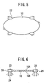
- the etching/cleaning apparatus comprises a wafer-rotating mechanism, as shown in Figs. 5 and 6.
- This mechanism which is of the roller-chucking type, includes four rollers 22 connected to corresponding rotational shafts 24.
- the rollers 22 are arranged at equal intervals along the periphery of the wafer 10 in the same horizontal plane.
- the wafer 10 is held, the wafer 10 is engaged with the recesses 26 of the four rollers 22 to be placed in the horizontal plane. Due to synchronous rotation of these rollers 22, the wafer 10 is rotated in the horizontal plane at a specific speed, as shown in Figs. 5 and 6.
- the number of the rollers 22 is four in this embodiment. However, it is not limited thereto. It is preferably set as a number ranging from 3 to 8.
- each roller 22 does not always contact with the end face 10C of the wafer 10 at the same position during operation.
- this mechanism is preferred for the etching or cleaning method of the wafer 10 according to the invention described later, where the whole end face 10C needs to be subjected to the etching or cleaning action.
- the location of the rollers 22 and the shafts 24 is fixed during operation, there is no possibility that the etching or cleaning liquid L E or L C emitted from the back nozzle 16 is blocked or stopped by the shafts 24. This means that there arises an additional advantage that the etching or cleaning liquid L E or L C is efficiently contacted with the back 10B of the wafer 10.
- the number of the edge nozzle 18 is one in the first embodiment, it is not limited thereto.
- the number of the nozzle 18 may be two or more according to the necessity.
- the wafer-holding mechanism of Figs. 5 and 6 is provided for holding the wafer 10 in a horizontal plane and for rotating the wafer 10 at a specific rotation speed.
- the surface nozzle 14 is provided for emitting the protecting liquid L P toward the surface center P1 of the wafer 10
- the back nozzle 16 is provided for emitting the etching or cleaning liquid L E or L C toward the back center P2 of the wafer 10
- the edge nozzle 18 is provided for emitting the etching or cleaning liquid L E or L C toward the edge of the wafer 10.
- the etching or cleaning liquid L E or L C emitted from the edge nozzle 18 is controlled to contact with the surface peripheral area 10E of the rotating wafer 10 and at the same time, the etching or cleaning liquid L E or L C emitted from the back nozzle 16 is controlled to contact entirely or partially with the back 10B of the same wafer 10.
- the protecting liquid L P emitted from the surface nozzle 14 is controlled to cover the entire device area 10D of the wafer 10 to protect the same against the etching or cleaning liquid L E or L C emitted from the edge nozzle 18.
- the surface peripheral area 10E, the end face 10C, and the back 10B of the wafer 10 can be effectively etched or cleaned to remove the undesired or unnecessary material(s) or contaminant(s) existing on the wafer 10, without applying any damages to the semiconductor device or elements and wiring lines in the device area 10D of the wafer 10.
- the etching or cleaning liquid L E or L C can be emitted from the edge nozzle 18 as a liquid beam or liquid fan toward the surface peripheral area 10E, the contact point of the liquid L E or L C with the area 10E can be set at satisfactory high precision.
- the device area 10D can be expanded toward the edge or end face 10C of the wafer 10, thereby making the width of the area 10E (i.e., the distance between the areas 10D and 10E) as short as possible (e.g., approximately 1.5 mm to 2.0 mm).
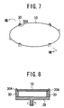
- Figs. 7 and 8 show schematically a wafer-holding mechanism used in an etching/cleaning apparatus according to a second embodiment, which is a variation of the mechanism.
- the other configuration of the apparatus according to the second embodiment is the same as that of the apparatus according to the first embodiment of Figs. 3 to 6.
- the explanation about the same configuration is omitted here for the sake of simplification.
- the wafer-holding mechanism is of the pin-chucking type, which includes four pins 30 joined to a rotational supporting member 28.
- the pins 30 are arranged at equal intervals along the circular edge of the member 28.
- Each pin 30 has a pocket 30A on which the edge of the wafer 10 is placed and engaged therewith.
- the wafer 10 is placed and held on the four pockets 30A of the pins 30.
- the wafer 10 is rotated in a horizontal plane due to the rotation of the member 28, as shown in Figs. 7 and 8.
- the number of the pins 30 is four in this embodiment. However, it is not limited thereto and it may take any number. It is preferably set as a number ranging from 3 to 8.
- each pins 30 is kept contacted with the end face 10C and the back 10B of the wafer 10 at the same position during operation.
- the chucking force of the wafer-holding mechanism is relaxed or released instantaneously and at the same time, the rotation speed is lowered a bit during operation.
- the rotating wafer 10 can be shifted in its holding position due to the inert force.
- the rotation of the wafer 10 may be temporarily stopped to lift the wafer 10 from the pins 30 with a proper handler (not shown) or the like.
- the holding position of the wafer 10 can be shifted or changed.
- two wafer-holding mechanisms of the pin-chucking type shown in Figs. 7 and 8 may be provided for supporting the wafer 10. In this case, a first one of the mechanisms is used to hold the wafer 10 and then, a second one of them is used therefor. Thus, the wafer 10 can be shifted in its holding position.
- the apparatus according to the second embodiment has the same advantages as those in the apparatus according to the first embodiment.
- the wafer-holding mechanism of Figs. 7 and 8 may be combined with the mechanism shown in Figs. 5 and 6.
- the rollers 22 may be contacted with the end face 10C of the wafer 10 during a front half of an etching or cleaning process and then, the pins 30 may be contacted with the end face 10C at different holding positions from those for the rollers 22 during a rear half of the process, and vice versa.
- the rotating wafer 10 can be shifted or switched in its holding position during the same process without means for shifting the holding position of the wafer 10.
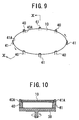
- Figs. 9 and 10 show schematically a wafer-holding mechanism used in an etching/cleaning apparatus according to a third embodiment, which is another variation of the mechanism. Because the other configuration of the apparatus according to the third embodiment is the same as that of the apparatus according to the first embodiment, the explanation about the same configuration is omitted here for the sake of simplification.
- the wafer-holding mechanism is of the pin-chucking type.
- This mechanism includes four pins 40 and four pins 41 joined to a rotational supporting member 38.
- the pins 40 and 41 are alternately arranged at equal intervals along the circular edge of the member 38.
- Each pin 40 has a pocket 40A on which the edge of the wafer 10 is placed and engaged therewith.
- Each pin 41 has a similar pocket 41A on which the edge of the wafer 10 is placed and engaged therewith.
- the wafer 10 is rotated, it is placed and held on the eight pockets 40A and 41A of the pins 40 and 41.
- the wafer 10 is rotated in a horizontal plane due to the rotation of the member 38, as shown in Figs. 9 and 10.
- the number of the pins 40 or 41 is four in this embodiment. However, it is not limited thereto and it may take any number. It is preferably set as 3.
- the four pins 40 are contacted with the end face 10C of the wafer 10 during a front half of an etching or cleaning process. Then, the four pins 41 are contacted with the end face 10C during a rear half of the process.
- the rotating wafer 10 can be shifted or switched in its holding position during the same process. There is an additional advantage that the means for shifting the holding position of the water 10 is unnecessary.
- the apparatus according to the third embodiment has the same advantages as those in the apparatus according to the first embodiment.
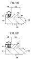
- Fig. 11 shows the process flow of forming Cu wiring lines using the damascene process and Figs. 12A to 12F show the steps thereof, respectively, in which an etching method and a cleaning method according to a fourth embodiment are included.
- any one of the above-explained etching/cleaning apparatuses according to the first to third embodiments may be used.
- a wiring trench is formed.
- a silicon dioxide (SiO 2 ) film 34 is formed on the surface 10A of the Si wafer 10 by a known method.
- the SiO 2 film 34 is formed to cover the whole device area 10D and to laterally protrude from the area 10D.
- the periphery or edge of the SiO 2 film 34 is located within the surface peripheral area 10E.
- the width of the surface peripheral area 10E is set as approximately 5 mm.
- a wiring trench 36 is formed in the SiO 2 film 34 to be located in the device area 10D by a known method.
- the state at this stage is shown in Fig. 12A.
- a barrier metal film and a seed Cu film are formed.
- the barrier metal film is used to prevent the Cu atoms from diffusing into the SiO 2 film 34 and/or the wafer 10.
- the seed Cu film is used to form a seed for plating.
- a barrier metal film 38 which is made of Ta, TaN, or the like, is formed on the SiO 2 film 34 to cover the trench 36 by sputtering.
- a seed Cu film 40 is formed on the barrier metal film 38 to cover the trench 36 by sputtering. The state at this stage is shown in Fig. 12B.
- the reference numeral 33 in Fig. 12B denotes a shield ring for preventing the sputtered species from being deposited on the surface peripheral area 10E and the end face 10C of the wafer 10.
- the shield ring 33 is placed on the wafer stage 31 during the sputtering process.
- a wiring Cu film is formed by electroplating. Specifically, a ring-shaped blocking member (i.e., a so-called O-ring, not shown) is placed on the SiO 2 film 34, forming a space on the seed Cu film 40. Then, a proper plating liquid or solution is supplied to the space, thereby forming a wiring Cu film 42 on the film 40, as shown in Fig. 12C.
- a ring-shaped blocking member i.e., a so-called O-ring, not shown
- the plating liquid usually leaks out of the O-ring.
- an unnecessary Cu film 44 is formed on the SiO 2 film 34 in the peripheral area 10E. This film 44 is easily detached from the film 34 and therefore, it will be a contaminant for the production lines. As a result, the film 44 must be removed prior to the next process.
- the unnecessary Cu film 44 is removed by etching using the above-explained etching/cleaning apparatus according to the first, second, or third embodiment. Since an etching liquid L E is supplied, the above-explained etching/cleaning apparatus serves as an etching apparatus.
- the wafer 10 with the films 34, 38, 40, 42, and 44 is held to be in a horizontal plane by the wafer-holding mechanism.
- a protecting liquid L P is emitted from the surface nozzle 14 toward the surface center P1 of the wafer 10, covering the whole device area 10D.
- any liquid having no etching action to Cu such as pure water or a water solution of any organic acid is used.
- a solution of an organic acid a solution of oxalic acid, citric acid, malonic acid, or the like is used, the concentration of which is preferably set as 0.001 % to 5 %. This is because these solutions are easily accessible, easily removed, and apply no damage to the device area 10D.
- pure water is used as the protecting liquid LP.
- an etching liquid L E is emitted from the edge nozzle 18 toward the edge of the wafer 10, covering the whole surface peripheral area 10E.
- the etching liquid L E any liquid having a large etch selectivity (Cu/SiO 2 ) is used, because the unnecessary Cu film 44 existing in the area 10E needs to be selectively etched while the SiO 2 film 34 is prevented from being etched.
- any acid or any alkali solution containing H 2 O 2 may be used.
- FPM HF/H 2 O 2 /H 2 O
- SPM H 2 SO 4 /H 2 O 2 /H 2 O
- HPM HCl/H 2 O 2 /H 2 O
- water solution of nitric hydrogen peroxide HCl/H 2 O 2 /H 2 O
- APM NH 4 OH/H 2 O 2 /H 2 O
- thick nitric acid (HNO 3 ), or the like is preferred. This is because these liquids provide satisfactorily high etch selectivity between Cu and SiO 2 and they are easily accessible.
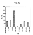
- the composition dependence of the etch selectivity (Cu/SiO 2 ) of FPM is shown in Fig. 13.
- FPM is used as the etching liquid P E emitted from the edge nozzle 18.
- pure water i.e., the protecting liquid L P
- FPM i.e., the etching liquid L E
- the pure water supplied to the vicinity of the surface center P1 of the wafer 10 automatically expands toward the edge of the wafer 10 along the surface 10A due to the centrifugal force, thereby covering the entire device area 10D.
- the FPM supplied in the surface peripheral area 10E moves toward the edge of the wafer 10 along the surface 10A due to the centrifugal force, thereby contacting with the entire area 10E.
- the FPM is emitted from the edge nozzle 18 as a beam.
- the contact point of the FPM beam with the surface 10A can be correctly adjusted, which realizes correct removal of the unnecessary Cu film 44 in the area 10E with satisfactory controllability.
- the state at this stage is shown in Fig. 12D, where the Cu film 44 is entirely removed and the edges of the films 38, 40, and 42 located outside the device area 10D are removed.
- the remaining wiring Cu film 42 in the device area 10D is annealed by a known method, thereby improving the quality of the film 42.
- a CMP process is carried out.
- a Cu wiring line 46 is formed in the trench 36 and at the sane time, the seed Cu film 40 and the barrier metal film 38 are left in the trench 36.
- a polishing waste 48 is attached on the surface 10A in the peripheral area 10E, on the end face 10C, and the back 10B of the wafer 10.
- the waste 48 is made of Cu and the barrier metal.
- the polishing waste 48 is removed using the above-explained etching/cleaning apparatus according to the first, second, or third embodiment. Since a cleaning liquid L C is supplied, the above-explained etching/cleaning apparatus serves as a cleaning apparatus.
- the wafer 10 is held on the wafer-holding mechanism.
- pure water i.e., the protecting liquid L P
- FPM i.e., the cleaning liquid L C
- FPM is emitted from the edge nozzle 18 toward the edge of the wafer 10 to cover the whole surface peripheral area 10E while FPM is emitted from the back nozzle 16 toward the back center P2 of the wafer 10 to cover the whole back 10B.
- the pure water supplied to the vicinity of the surface center P1 moves outward along the surface 10A due to the centrifugal force, covering and protecting the entire device area 10D.
- the FPM supplied to the surface peripheral area 10E moves toward the edge of the wafer 10 along the surface 10A to be dropped therefrom due to the centrifugal force, removing the polishing waste 48 existing in the area 10E and on the end face 10C.
- the surface peripheral area 10E and the end face 10C are fully cleaned.
- the FPM supplied to the vicinity of the back center P2 moves outward 10 along the back 10B to be dropped therefrom due to the centrifugal force, removing the polishing waste 48 existing on the back 10B.
- the back 10B of the wafer 10 is fully cleaned.
- the device area 10D is entirely covered with the pure water during the cleaning step S7, even if the FPM emitted from the nozzle 18 is slightly returned toward the device area 10D due to the rotational movement of the wafer 10, there is no possibility that the FPM is contacted with the device area 10D. As a result, the wiring Cu film 46 and the SiO 2 film 34 are prevented from being damaged by the FPM.
- any acid or any alkali solution containing H 2 O 2 may be used as the cleaning liquid L C . This is because H 2 O 2 has a good cleaning action of the polishing waste 48 of Cu.
- SPM, HPM, water solution of nitric hydrogen peroxide, APM, or thick nitric acid may be preferred. These are easily accessible, easily removable, and apply no damage to the device area 10D.
- a water solution of any organic acid that does not dissolves Cu may be used.
- a water solution of oxalic acid, citric acid, malonic acid, or the like may be used.
- the concentration of the organic acid solution is preferably set as 0.001 % to 5%.
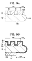
- Figs. 14A to 14F show the steps of a Cu wiring line formation process using the damascene process, respectively, which includes an etching method and a cleaning method according to a fifth embodiment.
- any one of the above-explained etching/cleaning apparatuses according to the first to third embodiments is used.
- the periphery of the area 10D is laterally shifted outward, thereby decreasing the width of the surface peripheral area 10E compared with the fourth embodiment.
- the other conditions are the same as those of the above-described fourth embodiment.
- a SiO 2 film 34 is formed on the surface 10A of the Si wafer 10 by a known method.
- the SiO 2 film 34 is formed to cover the whole device area 10D and to protrude slightly from the area 100.
- the periphery of the SiO 2 film 34 is located in the surface peripheral area 10E.
- the width of the surface peripheral area 10E is set as approximately 2 mm.
- wiring trenches 36 are formed in the SiO 2 film 34 to be located in the device area 10D by a known method.
- the state at this stage is shown in Fig. 14A.
- the wafer 10 is placed on a wafer stage 31' of a sputtering system.
- the stage 31' is smaller in size than the stage 31 used in the fourth embodiment.
- a barrier metal film 38 which is made of Ta, TaN, or the like, is formed on the SiO 2 film 34 to cover the trenches 36 by sputtering using the shield ring 33 (not shown).
- a seed Cu film 40 is formed on the barrier metal film 38 to cover the trenches 36 by sputtering without the shield ring 33.
- the state at this stage is shown in Fig. 14B.
- the seed Cu film 40 covers the whole end face 10C and part of the back 10B. This is because the width of the surface peripheral area 10E is very short and the shield ring 33 is not used.
- a ring-shaped blocking member i.e., a so-called O-ring, not shown
- a proper plating liquid or solution is supplied to the space to thereby form a wiring Cu film 42 on the film 40 by electroplating, as shown in Fig. 14C.
- an unnecessary Cu film 44 is additionally formed on the seed Cu film 40 in the peripheral area 10E, as shown in Fig. 14C.
- This film 44 may affect the performance of the semiconductor devices in the device area 10D and may be contaminants and as a result, it must be removed prior to the next process.
- step S4 first, the wafer 10 is held on the wafer-holding mechanism of the above-explained etching/cleaning apparatus according to the first, second, or third embodiment and then, it is rotated in a horizontal plane.
- pure water i.e., the protecting liquid L P
- FPM i.e., the etching liquid L E
- the wiring Cu film 40 existing in the surface peripheral area 10E, on the end face 10C, and in the back peripheral area 10F is entirely removed and at the same time, the seed Cu film 40 located outside the device area 10D is entirely removed.
- the state at this stage is shown in Fig. 14D.
- the remaining wiring Cu film 42 is annealed by a known method, thereby improving the quality of the film 42.
- a CMP process is carried out.
- Cu wiring lines 46 are formed in the trenches 36 and at the same time, the seed Cu film 40 and the barrier metal film 38 are left in the trenches 36.
- a polishing waste 48 is attached to the surface 10A in the peripheral area 10E, on the end face 10C, and the back 10B of the wafer 10, as shown in Fig. 14E.
- the waste 48 is made of Cu and the barrier metal.
- the polishing waste 48 is removed using the above-explained etching/cleaning apparatus according to the first, second, or third embodiment.
- the wafer 10 is held on the wafer-holding mechanism.
- pure water i.e., the protecting liquid L P
- the surface nozzle 14 is rotated in a horizontal plane by the mechanism.
- pure water i.e., the protecting liquid L P
- FPM i.e., the cleaning liquid L C
- the edge nozzle 18 toward the edge of the wafer 10 to cover the whole surface peripheral area 10E
- FPM is emitted from the back nozzle 16 toward the back center P2 of the wafer 10 to cover the whole back 10B.
- the pure water supplied to the vicinity of the surface center P1 of the wafer 10 moves outward, covering and protecting the entire device area 10D.
- the FPM supplied to the vicinity of the edge of the wafer 10 moves outward to be dropped therefrom, removing the polishing waste 48 existing in the surface peripheral area 10E and on the end face 10C.
- the FPM supplied to the vicinity of the back center P2 of the wafer 10 moves outward to be dropped therefrom, removing the polishing waste 48 existing on the back 10B.
- the surface peripheral area 10E, the end face 10C, and the back 10B of the wafer 10 are fully cleaned without damaging the device area 10D.
- the state at this stage is shown in Fig. 14F.
- the wafer 10 may be entirely cleaned in an additional process step by immersing entirely the wafer 10 into a cleaning solution or by brushing the wafer 10.
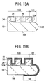
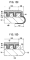
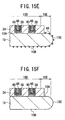
- Figs. 15A to 15F show the steps of a Cu wiring line formation process using the damascene process, respectively, which includes an etching method and a cleaning method according to a sixth embodiment.
- this process any one of the above-explained etching/cleaning apparatuses according to the first to third embodiments is used.
- both the barrier metal film 38 and the seed Cu film 40 are formed to partially cover the back 10B of the wafer 10. Similar to the fifth embodiment, the periphery of the area 10D is shifted outward compared with the fourth embodiment, thereby expanding the device area 14D and decreasing the width of the surface peripheral area 10E.
- a SiO 2 film 34 is formed on the surface 10A of the Si wafer 10 by a known method.
- the SiO 2 film 34 is formed to cover the whole device area 10D and to protrude slightly from the area 10D.
- the periphery of the SiO 2 film 34 is located in the surface peripheral area 10E.
- the width of the surface peripheral area 10E is set as approximately 2 mm.
- wiring trenches 36 are formed in the SiO 2 film 34 to be located in the device area 10D by a known method.
- the state at this stage is shown in Fig. 15A.
- a barrier metal film 38 which is made of Ta, TaN, or TaO x , is formed on the SiO 2 film 34 to cover the trenches 36 by sputtering.
- a seed Cu film 40 is formed on the barrier metal film 38 to cover the trenches 36 by sputtering. The state at this stage is shown in Fig. 15B.
- both the barrier metal film 38 and the seed Cu film 40 extend to the back 10B of the wafer 10. This state may be caused by sputtering without the shield ring 33 and setting the width of the surface peripheral area 10E as very short.
- step S3 an O-ring (not shown) is placed on the seed Cu film 40 to form a space on the film 40. Then, a proper plating liquid or solution is supplied to the space to form a wiring Cu film 42 on the film 40 by electroplating, as shown in Fig. 15C.
- an unnecessary Cu film 44 is additionally formed on the seed Cu film 40 in the peripheral area 10E.
- the wafer 10 is rotated in a horizontal plane.
- pure water is emitted from the surface nozzle 14 toward the surface center P1 of the rotating wafer 10, covering the whole device area 10D.
- FPM is emitted from the edge nozzle 18 toward the edge of the wafer 10, contacting the FPM with the whole surface peripheral area 10E.
- FPM is emitted from the back nozzle 16 toward the back center P2 of the wafer 10, contacting the FPM with the whole back 10B.
- the undesired Cu film 44 existing in the surface peripheral area 10E, on the end face 10C, and in the back peripheral area 10F is entirely removed and at the same time, the seed Cu film 40 located outside the device area 10D is entirely removed.
- etching liquid L E hydrofluoric acid
- the remaining wiring Cu film 42 is annealed by a known method, thereby improving the quality of the film 42.
- a CMP process is carried out.
- Cu wiring lines 46 are formed in the trenches 36 and at the same time, the seed Cu film 40 and the barrier metal film 38 are left in the trenches 36.
- a polishing waste 48 is attached on the surface 10A in the peripheral area 10E, on the end face 10C, and on the back 10B of the wafer 10, as shown in Fig. 15E.
- the polishing waste 48 is removed using the above-explained etching/cleaning apparatus according to the first, second, or third embodiment. Specifically, first, the wafer 10 is held on the wafer-holding mechanism. Next, while the wafer 10 is rotated in a horizontal plane, pure water is emitted from the surface nozzle 14 toward the surface center P1 of the wafer 10, covering the whole device area 10D. At the same time as this, FPM is emitted from the edge nozzle 18 toward the edge of the wafer 10 to be contacted with the whole surface peripheral area 10E while FPM is emitted from the back nozzle 16 toward the back center P2 of the wafer 10 to be contacted with the whole back 10B. Thus, the surface peripheral area 10E, the end face 10C, and the back 10B of the wafer 10 are fully cleaned. The state at this stage is shown in Fig. 15F.
- the Cu wiring lines 46 are formed in the trenches 36 of the SiO 2 film 34.
- the present invention is not limited thereto. It can be applied to any case if at least one of the etching and cleaning processes for a semiconductor wafer is necessary.
- the invention may be applied to the case where metal wiring lines or metal electrodes made of Pt, Ir, IrO, or the like, are formed on a dielectric film.
- the invention may be applied to the case where a ferroelectric film made of BST, PZT, or the like, is formed on another film.
Landscapes
- Chemical & Material Sciences (AREA)
- Chemical Kinetics & Catalysis (AREA)
- General Chemical & Material Sciences (AREA)
- Engineering & Computer Science (AREA)
- Materials Engineering (AREA)
- Mechanical Engineering (AREA)
- Metallurgy (AREA)
- Organic Chemistry (AREA)
- Cleaning Or Drying Semiconductors (AREA)
- Weting (AREA)
- Cleaning By Liquid Or Steam (AREA)
- ing And Chemical Polishing (AREA)
Abstract
Description
Claims (49)
- An etching apparatus comprising:(a) a rotating means for holding a semiconductor wafer and for rotating said wafer in a horizontal plane;said wafer having a device area and a surface peripheral area on its surface;said surface peripheral area being located outside said device area; and(b) an edge nozzle for emitting an etching liquid toward a surface peripheral area of said wafer;
wherein said etching liquid emitted from said edge nozzle selectively etches out an unnecessary material existing in said surface peripheral area of said wafer. - The apparatus according to claim 1, wherein said etching liquid emitted from said edge nozzle has an emission direction oriented along a rotation direction of said wafer or outward with respect to a tangent of said wafer formed near a contact point of said liquid with said surface peripheral area of said wafer.
- The apparatus according to claim 1, further comprising a back nozzle for emitting an etching liquid toward a back center of said wafer;
wherein said etching liquid emitted from said back nozzle etches out an unnecessary material existing on a back of said wafer. - The apparatus according to claim 1, further comprising a surface nozzle for emitting a protecting liquid toward a surface center of said wafer;
wherein said protecting liquid emitted from said surface nozzle covers said device area of said wafer to protect the same against said etching liquid emitted from said edge nozzle. - The apparatus according to claim 1, further comprising a back nozzle for emitting an etching liquid toward a back center of said wafer and a surface nozzle for emitting protecting liquid toward a surface center of said wafer;
wherein said etching liquid emitted from said back nozzle etches out an unnecessary material existing on a back of said wafer, and said protecting liquid emitted from said surface nozzle covers said device area of said wafer to protect the same against said etching liquid emitted from said edge nozzle. - The apparatus according to claim 1, wherein said etching liquid emitted from said edge nozzle is beam-shaped.
- The apparatus according to claim 1, wherein said rotating means is of a roller-chucking type, in which said means comprises rollers arranged along an end face of said wafer, and said rollers are contacted with said end face of said wafer to hold said wafer and rotated synchronously.
- The apparatus according to claim 1, wherein said rotating means is of a pin-chucking type, in which said means comprises pins supported by a supporting member and arranged along an end face of said wafer, and said pins are contacted with said end face of said wafer to hold said wafer and rotated synchronously by said member.
- The apparatus according to claim 1, wherein said rotating means is of a pin-chucking type, in which said means comprises a first plurality of pins and a second plurality of pins supported by a supporting member;
wherein said first plurality of pins and said second plurality of pins are alternately arranged along an end face of said wafer;
wherein said first plurality of pins and said second plurality of pins are alternately contacted with said end face of said wafer to hold said wafer and rotated synchronously by said member. - The apparatus according to claim 1, wherein said rotating means comprises a first plurality of pins and a second plurality of pins supported by a supporting member;
wherein said first plurality of pins are arranged along an end face of said wafer and said second plurality of pins are arranged along said end face of said wafer;
and wherein said first plurality of pins are contacted with said end face of said wafer to hold said wafer and rotated synchronously by said member in a period, and said second plurality of pins are contacted with said end face of said wafer to hold said wafer and rotated synchronously by said member in another period. - The apparatus according to claim 1, wherein the distance of an end of said edge nozzle from a point where a longitudinal axis of said edge nozzle intersects said surface of said wafer is set as a value in the range of 1 mm to 50 mm, and the angle of said edge nozzle with respect to a tangent of said wafer at said point is set as a value in the range of 0° to 90°.
- The apparatus according to claim 3, wherein the distance of an end of said back nozzle from said back center of said wafer is set as a value in the range of 70 mm to 200 mm, and the angle of said back nozzle with respect to said back of said wafer is set as a value in the range of 15° to 60°.
- The apparatus according to claim 4, wherein the distance of an end of said surface nozzle from said surface center of said wafer is set as a value in the range of 70 mm to 200 mm, and the angle of said surface nozzle with respect to said surface of said wafer is set as a value in the range of 15° to 60°.
- A cleaning apparatus comprising:(a) a rotating means for holding a semiconductor wafer and for rotating said wafer in a horizontal plane;said wafer having a device area and a surface peripheral area on its surface;said surface peripheral area being located outside said device area; and(b) an edge nozzle for emitting a cleaning liquid toward a surface peripheral area of said wafer;
wherein said cleaning liquid emitted from said edge nozzle selectively removes an unnecessary material existing in said surface peripheral area of said wafer. - The apparatus according to claim 14, wherein said cleaning liquid emitted from said edge nozzle has an emission direction oriented along a rotation direction of said wafer or outward with respect to a tangent of said wafer formed near a contact point of said liquid with said surface peripheral area of said wafer.
- The apparatus according to claim 14, further comprising a back nozzle for emitting a cleaning liquid toward a back center of said wafer;
wherein said cleaning liquid emitted from said back nozzle removes an unnecessary material existing on a back of said wafer. - The apparatus according to claim 14, further comprising a surface nozzle for emitting a protecting liquid toward a surface center of said wafer;
wherein said protecting liquid emitted from said surface nozzle covers said device area of said wafer to protect the same against said cleaning liquid emitted from said edge nozzle. - The apparatus according to claim 14, further comprising a back nozzle for emitting a cleaning liquid toward a back center of said wafer and a surface nozzle for emitting protecting liquid toward a surface center of said wafer;
wherein said cleaning liquid emitted from said back nozzle etches out an unnecessary material existing on a back of said wafer, and said protecting liquid emitted from said surface nozzle covers said device area of said wafer to protect the same against said cleaning liquid emitted from said edge nozzle. - The apparatus according to claim 14, wherein said cleaning liquid emitted from said edge nozzle is beam-shaped.
- The apparatus according to claim 14, wherein said rotating means is of a roller-chucking type, in which said means comprises rollers arranged along an end face of said wafer, and said rollers are contacted with said end face of said wafer to hold said wafer and rotated synchronously.
- The apparatus according to claim 14, wherein said rotating means is of a pin-chucking type, in which said means comprises pins supported by a supporting member and arranged along an end face of said wafer, and said pins are contacted with said end face of said wafer to hold said wafer and rotated synchronously by said member.
- The apparatus according to claim 14, wherein said rotating means is of a pin-chucking type, in which said means comprises a first plurality of pins and a second plurality of pins supported by a supporting member;
wherein said first plurality of pins and said second plurality of pins are alternately arranged along an end face of said wafer;
wherein said first plurality of pins and said second plurality of pins are alternately contacted with said end face of said wafer to hold said wafer and rotated synchronously by said member. - The apparatus according to claim 14, wherein said rotating means comprises a first plurality of pins and a second plurality of pins supported by a supporting member;
wherein said first plurality of pins are arranged along an end face of said wafer and said second plurality of pins are arranged along said end face of said wafer;
and wherein said first plurality of pins are contacted with said end face of said wafer to hold said wafer and rotated synchronously by said member in a period, and said second plurality of pins are contacted with said end face of said wafer to hold said wafer and rotated synchronously by said member in another period. - The apparatus according to claim 14, wherein the distance of an end of said edge nozzle from a point where a longitudinal axis of said edge nozzle intersects said surface of said wafer is set as a value in the range of 1 mm to 50 mm, and the angle of said edge nozzle with respect to a tangent of said wafer at said point is set as a value in the range of 0° to 90°.
- The apparatus according to claim 16, wherein the distance of an end of said back nozzle from said back center of said wafer is set as a value in the range of 70 mm to 200 mm, and the angle of said back nozzle with respect to said back of said wafer is set as a value in the range of 15° to 60°.
- The apparatus according to claim 17, wherein the distance of an end of said surface nozzle from said surface center of said wafer is set as a value in the range of 70 mm to 200 mm, and the angle of said surface nozzle with respect to said surface of said wafer is set as a value in the range of 15° to 60°.
- An etching method comprising the steps of:(a) rotating a semiconductor wafer in a horizontal plane;said wafer having a device area and a surface peripheral area on its surface;said surface peripheral area being located outside said device area; and(b) emitting an etching liquid toward a surface peripheral area of said wafer by an edge nozzle, thereby selectively etching out an unnecessary material existing in said surface peripheral area.
- The method according to claim 27, wherein said etching liquid emitted from said edge nozzle has an emission direction oriented along a rotation direction of said wafer or outward with respect to a tangent of said wafer formed near a contact point of said liquid with said surface peripheral area of said wafer.
- The method according to claim 27, wherein an etching liquid is emitted toward a back center of said wafer by a back nozzle, thereby etching out an unnecessary material existing on a back of said wafer.
- The method according to claim 27, wherein a protecting liquid is emitted toward a surface center of said wafer by a surface nozzle, thereby covering said device area of said wafer to protect the same against said etching liquid emitted from said edge nozzle.
- The method according to claim 27, wherein an etching liquid is emitted toward a back center of said wafer by a back nozzle, thereby etching out an unnecessary material existing on a back of said wafer, and a protecting liquid is emitted toward a surface center of said wafer by a surface nozzle, thereby covering said device area of said wafer to protect the same against said etching liquid emitted from said edge nozzle.
- The method according to claim 27, wherein said etching liquid emitted from said edge nozzle is beam-shaped.
- The method according to claim 27, wherein an acid or an alkali solution containing H2O2 is used as said etching liquid.
- The method according to claim 27, wherein said unnecessary material is Cu;
and wherein said etching liquid is one selected from the group consisting of FPM (HF/H2O2/H2O), SW (H2SO4/H2O2/H2O), HPM (HCl/H2O2/H2O), water solution of nitric hydrogen peroxide (HNO3/H2O2/H2O), APM (NH4OH/H2O2/H2O), and thick nitric acid (HNO3). - The method according to claim 34, wherein a SiO2 film is formed on or over said surface of said wafer;
and wherein etching liquid has a composition ofHF : H2O2 : H2O = 1-10 : 1-20 : 100H2SO4 : H2O2 : H2O = 1-10 : 1-20 : 100HCl : H2O2 : H2O = 1-10 : 1-20 : 100HNO3 : H2O2 : H2O = 1-10 : 1-20 : 100NH4OH : H2O2 : H2O = 1-10 : 1-20 : 100HNO3 = 30% - 80%. - The method according to claim 34, wherein a SiO2 film is formed on or over said surface of said wafer;
and wherein etching liquid is FPM having a composition of HF : H2O2 : H2O = 1 : 10 : 100. - The method according to claim 27, wherein pure water or a water solution of organic acid is used as said protecting liquid.
- The method according to claim 37, wherein said water solution of organic acid is a water solution of one selected from the group consisting of oxalic acid, citric acid, and malonic acid;
and wherein said solution of organic acid has a concentration of 0.001 % to 5 %. - The method according to claim 27, wherein said unnecessary material is Ta, TaN, or TaOx;
and wherein hydrofluoric acid (HF) is used as said etching liquid. - A cleaning method comprising the steps of:(a) rotating a semiconductor wafer in a horizontal plane;said wafer having a device area and a surface peripheral area on its surface;said surface peripheral area being located outside said device area; and(b) emitting a cleaning liquid toward a surface peripheral area of said wafer by an edge nozzle, thereby selectively removing an unnecessary material existing in said surface peripheral area.
- The method according to claim 40, wherein said cleaning liquid emitted from said edge nozzle has an emission direction oriented along a rotation direction of said wafer or outward with respect to a tangent of said wafer formed near a contact point of said liquid with said surface peripheral area of said wafer.
- The method according to claim 40, wherein a cleaning liquid is emitted toward a back center of said wafer by a back nozzle, thereby etching out an unnecessary material existing on a back of said wafer.
- The method according to claim 40, wherein a protecting liquid is emitted toward a surface center of said wafer by a surface nozzle, thereby covering said device area of said wafer to protect the same against said cleaning liquid emitted from said edge nozzle.
- The method according to claim 40, wherein a cleaning liquid is emitted toward a back center of said wafer by a back nozzle, thereby removing an unnecessary material existing on a back of said wafer, and a protecting liquid is emitted toward a surface center of said wafer by a surface nozzle, thereby covering said device area of said wafer to protect the same against said cleaning liquid emitted from the said nozzle.
- The method according to claim 40, wherein said cleaning liquid emitted from said edge nozzle is beam-shaped.
- The method according to claim 40, wherein an acid or an alkali solution containing H2O2 is used as said cleaning liquid.
- The method according to claim 40, wherein said unnecessary material is Cu;
and wherein said cleaning liquid is one selected from the group consisting of FPM (HF/H2O2/H2O), SPM (H2SO2/H2O2/H2O), HPM (HCl/H2O2/H2O), water solution of nitric hydrogen peroxide (HNO3/H2O2/H2O), APM (NH4OH/H2O2/H2O), and thick nitric acid (HNO3). - The method according to claim 40, wherein pure water or a water solution of organic acid is used as said protecting liquid.
- The method according to claim 48, wherein said water solution of organic acid is a water solution of one selected from the group consisting of oxalic acid, citric acid, and malonic acid;
and wherein said solution of organic acid has a concentration of 0.001 % to 5 %.
Applications Claiming Priority (2)
| Application Number | Priority Date | Filing Date | Title |
|---|---|---|---|
| JP6889899 | 1999-03-15 | ||
| JP06889899A JP3395696B2 (en) | 1999-03-15 | 1999-03-15 | Wafer processing apparatus and wafer processing method |
Publications (3)
| Publication Number | Publication Date |
|---|---|
| EP1037261A2 true EP1037261A2 (en) | 2000-09-20 |
| EP1037261A3 EP1037261A3 (en) | 2002-11-06 |
| EP1037261B1 EP1037261B1 (en) | 2006-05-17 |
Family
ID=13386944
Family Applications (1)
| Application Number | Title | Priority Date | Filing Date |
|---|---|---|---|
| EP00104585A Expired - Lifetime EP1037261B1 (en) | 1999-03-15 | 2000-03-14 | Etching and cleaning method and etching and cleaning apparatus used therefor |
Country Status (6)
| Country | Link |
|---|---|
| US (4) | US6683007B1 (en) |
| EP (1) | EP1037261B1 (en) |
| JP (1) | JP3395696B2 (en) |
| CN (1) | CN1157767C (en) |
| DE (1) | DE60027946T2 (en) |
| TW (1) | TW561536B (en) |
Cited By (15)
| Publication number | Priority date | Publication date | Assignee | Title |
|---|---|---|---|---|
| EP1091811A4 (en) * | 1998-03-13 | 2002-01-30 | Semitool Inc | Selective treatment of the surface of a microelectronic workpiece |
| WO2003032380A1 (en) * | 2001-10-03 | 2003-04-17 | Ebara Corporation | Device and method for processing substrate |
| WO2003034479A1 (en) * | 2001-10-16 | 2003-04-24 | Ebara Corporation | Substrate processing apparatus |
| US6586161B2 (en) | 1999-08-31 | 2003-07-01 | Hitachi, Ltd. | Mass production method of semiconductor integrated circuit device and manufacturing method of electronic device |
| DE10319521A1 (en) * | 2003-04-30 | 2004-11-25 | Scp Germany Gmbh | Method and device for treating disc-shaped substrates |
| US7090751B2 (en) | 2001-08-31 | 2006-08-15 | Semitool, Inc. | Apparatus and methods for electrochemical processing of microelectronic workpieces |
| US7102763B2 (en) | 2000-07-08 | 2006-09-05 | Semitool, Inc. | Methods and apparatus for processing microelectronic workpieces using metrology |
| US7264698B2 (en) | 1999-04-13 | 2007-09-04 | Semitool, Inc. | Apparatus and methods for electrochemical processing of microelectronic workpieces |
| US7438788B2 (en) | 1999-04-13 | 2008-10-21 | Semitool, Inc. | Apparatus and methods for electrochemical processing of microelectronic workpieces |
| EP1589568A3 (en) * | 1998-03-13 | 2009-02-25 | Semitool, Inc. | Selective treatment of the surface of a microelectronic workpiece |
| US7566386B2 (en) | 1999-04-13 | 2009-07-28 | Semitool, Inc. | System for electrochemically processing a workpiece |
| EP2838111A1 (en) * | 2013-08-14 | 2015-02-18 | Applied Materials, Inc. | Methods for cleaning a wafer edge including a notch |
| US20150162207A1 (en) * | 2013-12-06 | 2015-06-11 | Tel Fsi, Inc. | Method of using separate wafer contacts during wafer processing |
| CN111463152A (en) * | 2020-04-17 | 2020-07-28 | 重庆芯洁科技有限公司 | High-pressure washing equipment for semiconductor substrate and using method thereof |
| US20220084846A1 (en) * | 2018-09-10 | 2022-03-17 | Toshiba Memory Corporation | Semiconductor manufacturing apparatus and method for manufacturing semiconductor device |
Families Citing this family (102)
| Publication number | Priority date | Publication date | Assignee | Title |
|---|---|---|---|---|
| US6413436B1 (en) * | 1999-01-27 | 2002-07-02 | Semitool, Inc. | Selective treatment of the surface of a microelectronic workpiece |
| US20050217707A1 (en) * | 1998-03-13 | 2005-10-06 | Aegerter Brian K | Selective processing of microelectronic workpiece surfaces |
| JP3395696B2 (en) | 1999-03-15 | 2003-04-14 | 日本電気株式会社 | Wafer processing apparatus and wafer processing method |
| US6516815B1 (en) * | 1999-07-09 | 2003-02-11 | Applied Materials, Inc. | Edge bead removal/spin rinse dry (EBR/SRD) module |
| JP4584385B2 (en) * | 1999-08-10 | 2010-11-17 | 大日本スクリーン製造株式会社 | Substrate processing apparatus and substrate processing method |
| US20020018172A1 (en) * | 2000-02-10 | 2002-02-14 | Alwan James J. | Method for manufacturing a flat panel display using localized wet etching |
| JP2001319919A (en) * | 2000-05-08 | 2001-11-16 | Tokyo Electron Ltd | Semiconductor device manufacturing method and processing apparatus |
| JP2001319849A (en) * | 2000-05-08 | 2001-11-16 | Tokyo Electron Ltd | Liquid processing apparatus and liquid processing method |
| JP2002134717A (en) * | 2000-10-25 | 2002-05-10 | Sony Corp | Method for manufacturing semiconductor device |
| JP2002313757A (en) | 2001-04-17 | 2002-10-25 | Hitachi Ltd | Method for manufacturing semiconductor integrated circuit device |
| JP4743735B2 (en) * | 2001-05-30 | 2011-08-10 | 大日本スクリーン製造株式会社 | Substrate processing apparatus and substrate processing method |
| JP3511514B2 (en) * | 2001-05-31 | 2004-03-29 | エム・エフエスアイ株式会社 | Substrate purification processing apparatus, dispenser, substrate holding mechanism, substrate purification processing chamber, and substrate purification method using these |
| JP3958539B2 (en) * | 2001-08-02 | 2007-08-15 | 東京エレクトロン株式会社 | Substrate processing apparatus and substrate processing method |
| US6709875B2 (en) * | 2001-08-08 | 2004-03-23 | Agilent Technologies, Inc. | Contamination control for embedded ferroelectric device fabrication processes |
| JP4803625B2 (en) * | 2001-09-04 | 2011-10-26 | ルネサスエレクトロニクス株式会社 | Manufacturing method of semiconductor device |
| TW561516B (en) * | 2001-11-01 | 2003-11-11 | Tokyo Electron Ltd | Substrate processing apparatus and substrate processing method |
| US6855640B2 (en) * | 2002-02-26 | 2005-02-15 | Institute Of Microelectronics | Apparatus and process for bulk wet etch with leakage protection |
| KR100481277B1 (en) * | 2002-05-10 | 2005-04-07 | 한국디엔에스 주식회사 | Device and Method for manufacturing semiconductor |
| KR100468529B1 (en) * | 2002-05-18 | 2005-01-27 | 엘지.필립스 엘시디 주식회사 | etchant coating apparatus and wet etching method using thereof |
| US7320942B2 (en) * | 2002-05-21 | 2008-01-22 | Applied Materials, Inc. | Method for removal of metallic residue after plasma etching of a metal layer |
| US7018555B2 (en) * | 2002-07-26 | 2006-03-28 | Dainippon Screen Mfg. Co., Ltd. | Substrate treatment method and substrate treatment apparatus |
| JP4365605B2 (en) * | 2002-07-26 | 2009-11-18 | 大日本スクリーン製造株式会社 | Substrate holding apparatus and substrate holding method, and substrate processing apparatus and substrate processing method using the same |
| TWI233157B (en) * | 2002-09-17 | 2005-05-21 | M Fsi Ltd | Regeneration process of etching solution, etching process, and etching system |
| TWI231950B (en) * | 2002-11-28 | 2005-05-01 | Tokyo Electron Ltd | Substrate processing apparatus and cleaning method |
| JP2004207454A (en) * | 2002-12-25 | 2004-07-22 | Renesas Technology Corp | Method for manufacturing semiconductor device |
| DE10326273B4 (en) * | 2003-06-11 | 2008-06-12 | Advanced Micro Devices, Inc., Sunnyvale | Method for reducing disc contamination by removing metallization pad layers at the wafer edge |
| US7078160B2 (en) * | 2003-06-26 | 2006-07-18 | Intel Corporation | Selective surface exposure, cleans, and conditioning of the germanium film in a Ge photodetector |
| US7476290B2 (en) * | 2003-10-30 | 2009-01-13 | Ebara Corporation | Substrate processing apparatus and substrate processing method |
| US20050112279A1 (en) * | 2003-11-24 | 2005-05-26 | International Business Machines Corporation | Dynamic release wafer grip and method of use |
| JP2005183937A (en) * | 2003-11-25 | 2005-07-07 | Nec Electronics Corp | Semiconductor device manufacturing method and resist removal cleaning apparatus |
| JP2005217320A (en) * | 2004-01-30 | 2005-08-11 | Renesas Technology Corp | Method for forming wiring, fabrication process of semiconductor device and process for manufacturing semiconductor packaging equipment |
| JP2005235978A (en) * | 2004-02-19 | 2005-09-02 | Sony Corp | Semiconductor device and manufacturing method of semiconductor device |
| JP2007523463A (en) * | 2004-02-24 | 2007-08-16 | 株式会社荏原製作所 | Substrate processing apparatus and method |
| JP2005327807A (en) * | 2004-05-12 | 2005-11-24 | Sony Corp | Single wafer cleaning device and cleaning method thereof |
| KR100618868B1 (en) * | 2004-10-19 | 2006-08-31 | 삼성전자주식회사 | Spin device |
| TW200625437A (en) * | 2004-12-30 | 2006-07-16 | Macronix Int Co Ltd | Shallow trench isolation process of forming smooth edge angle by cleaning procedure |
| JP4613709B2 (en) * | 2005-06-24 | 2011-01-19 | セイコーエプソン株式会社 | Manufacturing method of semiconductor device |
| US20070072426A1 (en) * | 2005-09-26 | 2007-03-29 | Tzu-Yu Tseng | Chemical mechanical polishing process and apparatus therefor |
| JP2006139271A (en) * | 2005-10-24 | 2006-06-01 | Hoya Corp | Apparatus and method for removing unwanted film, and method for manufacturing photomask blank |
| JP4793927B2 (en) | 2005-11-24 | 2011-10-12 | 東京エレクトロン株式会社 | Substrate processing method and apparatus |
| JP4698407B2 (en) | 2005-12-20 | 2011-06-08 | 大日本スクリーン製造株式会社 | Substrate processing apparatus and substrate processing method |
| JP4708243B2 (en) * | 2006-03-28 | 2011-06-22 | 東京エレクトロン株式会社 | Liquid processing apparatus, liquid processing method, and computer-readable storage medium |
| WO2008005517A1 (en) * | 2006-07-07 | 2008-01-10 | Accretech Usa, Inc. | Processing chamber having labyrinth seal |
| KR101353490B1 (en) * | 2006-07-20 | 2014-01-27 | 에프엔에스테크 주식회사 | Processing apparatus for substrate |
| KR100829923B1 (en) * | 2006-08-30 | 2008-05-16 | 세메스 주식회사 | Spin head and substrate processing method using same |
| US20080060683A1 (en) * | 2006-09-08 | 2008-03-13 | Arvidson Aaron W | Apparatus and methods for cleaning a wafer edge |
| KR101387711B1 (en) * | 2007-04-10 | 2014-04-23 | 에프엔에스테크 주식회사 | Glass substrate etching apparatus of flat panel display |
| KR20090005489A (en) * | 2007-07-09 | 2009-01-14 | 삼성전자주식회사 | Semiconductor wet etchant and wiring structure formation method using the same |
| JP4966116B2 (en) * | 2007-07-09 | 2012-07-04 | ルネサスエレクトロニクス株式会社 | Manufacturing method of semiconductor integrated circuit device |
| US8734661B2 (en) * | 2007-10-15 | 2014-05-27 | Ebara Corporation | Flattening method and flattening apparatus |
| JP5036614B2 (en) * | 2008-04-08 | 2012-09-26 | 東京応化工業株式会社 | Substrate stage |
| JP2011040419A (en) * | 2008-05-22 | 2011-02-24 | Fuji Electric Systems Co Ltd | Method for manufacturing semiconductor device and apparatus therefor |
| JP4848402B2 (en) * | 2008-08-20 | 2011-12-28 | ルネサスエレクトロニクス株式会社 | Manufacturing method of semiconductor integrated circuit device |
| KR101017654B1 (en) | 2008-11-26 | 2011-02-25 | 세메스 주식회사 | Substrate chucking member, substrate processing apparatus having same and substrate processing method using same |
| JP2010206056A (en) * | 2009-03-05 | 2010-09-16 | Renesas Electronics Corp | Method of manufacturing semiconductor integrated circuit device |
| DE102009050845A1 (en) * | 2009-10-19 | 2011-04-21 | Gebr. Schmid Gmbh & Co. | Method and device for treating a substrate surface of a substrate |
| US8324105B2 (en) * | 2010-08-13 | 2012-12-04 | Victory Gain Group Corporation | Stacking method and stacking carrier |
| CN102140669B (en) * | 2011-03-17 | 2016-06-01 | 上海集成电路研发中心有限公司 | Cleaning method after silicon chip electroplating copper |
| US9421617B2 (en) | 2011-06-22 | 2016-08-23 | Tel Nexx, Inc. | Substrate holder |
| US9117856B2 (en) | 2011-07-06 | 2015-08-25 | Tel Nexx, Inc. | Substrate loader and unloader having an air bearing support |
| CN103014708A (en) * | 2011-09-21 | 2013-04-03 | 沈阳黎明航空发动机(集团)有限责任公司 | Single crystal blade surface grain etching method |
| CN103084349A (en) * | 2011-11-03 | 2013-05-08 | 无锡华润上华科技有限公司 | Wafer cleaning method |
| CN103123904B (en) * | 2011-11-21 | 2015-11-25 | 无锡华润上华科技有限公司 | A kind of pre-treating method measuring silicon chip surface metal impurities |
| CN103128073A (en) * | 2011-12-01 | 2013-06-05 | 无锡华润上华科技有限公司 | Wafer washing method, wafer washing device and wafer |
| JP6130995B2 (en) * | 2012-02-20 | 2017-05-17 | サンケン電気株式会社 | Epitaxial substrate and semiconductor device |
| JP6084376B2 (en) * | 2012-06-19 | 2017-02-22 | 武蔵エンジニアリング株式会社 | Cleaning device and cleaning method for liquid material discharge device |
| JP6054343B2 (en) * | 2012-08-07 | 2016-12-27 | 東京エレクトロン株式会社 | Substrate cleaning apparatus, substrate cleaning system, substrate cleaning method, and storage medium |
| JP5586734B2 (en) | 2012-08-07 | 2014-09-10 | 東京エレクトロン株式会社 | Substrate cleaning apparatus, substrate cleaning system, substrate cleaning method, and storage medium |
| CN103021831A (en) * | 2012-12-03 | 2013-04-03 | 天津中环领先材料技术有限公司 | Processing method of monocrystalline silicon corrosion piece with long minority carrier service life |
| CN104078352B (en) * | 2013-03-27 | 2017-06-27 | 中芯国际集成电路制造(上海)有限公司 | Method for cleaning wafer and wafer cleaning device |
| JP2015005660A (en) * | 2013-06-21 | 2015-01-08 | 東京エレクトロン株式会社 | Method and apparatus for removing tantalum oxide film |
| CN103346108A (en) * | 2013-06-27 | 2013-10-09 | 上海华力微电子有限公司 | Device and method for improving smoothness of wafer edge |
| JP6600470B2 (en) | 2014-04-01 | 2019-10-30 | 株式会社荏原製作所 | Cleaning device and cleaning method |
| CN104971916B (en) * | 2014-04-01 | 2020-07-07 | 株式会社荏原制作所 | Cleaning device and cleaning method |
| DE102014013591A1 (en) | 2014-09-13 | 2016-03-17 | Jörg Acker | Process for the preparation of silicon surfaces with low reflectivity |
| JP6341035B2 (en) * | 2014-09-25 | 2018-06-13 | 東京エレクトロン株式会社 | Substrate liquid processing method, substrate liquid processing apparatus, and storage medium |
| KR101621482B1 (en) * | 2014-09-30 | 2016-05-17 | 세메스 주식회사 | Apparatus and Method for treating substrate |
| JP6618334B2 (en) * | 2015-06-03 | 2019-12-11 | 株式会社Screenホールディングス | Substrate processing apparatus, film forming unit, substrate processing method, and film forming method |
| WO2016194285A1 (en) | 2015-06-03 | 2016-12-08 | 株式会社Screenホールディングス | Substrate processing apparatus, film forming unit, substrate processing method and film forming method |
| JP2017098367A (en) * | 2015-11-20 | 2017-06-01 | 東京エレクトロン株式会社 | Substrate processing method |
| US9768017B1 (en) * | 2016-03-15 | 2017-09-19 | United Microelectronics Corporation | Method of epitaxial structure formation in a semiconductor |
| WO2017170714A1 (en) * | 2016-03-29 | 2017-10-05 | 新日鐵住金株式会社 | Liquid removal apparatus and liquid removal method |
| JP6815799B2 (en) * | 2016-09-13 | 2021-01-20 | 東京エレクトロン株式会社 | Substrate processing equipment and substrate processing method |
| TW201828356A (en) * | 2016-10-26 | 2018-08-01 | 日商東京威力科創股份有限公司 | Liquid treatment method and liquid treatment device |
| JP6386113B2 (en) * | 2017-02-07 | 2018-09-05 | 芝浦メカトロニクス株式会社 | Spin processing equipment |
| JP7160624B2 (en) * | 2018-10-17 | 2022-10-25 | 株式会社Screenホールディングス | SUBSTRATE PROCESSING APPARATUS AND SUBSTRATE PROCESSING METHOD |
| JP7241594B2 (en) * | 2019-04-22 | 2023-03-17 | 東京エレクトロン株式会社 | Substrate processing method and substrate processing apparatus |
| KR102815121B1 (en) | 2019-07-05 | 2025-06-04 | 후지필름 가부시키가이샤 | Method of processing compositions, kits and substrates |
| JP7170608B2 (en) * | 2019-09-09 | 2022-11-14 | 三菱電機株式会社 | WAFER CLEANING APPARATUS AND SEMICONDUCTOR DEVICE MANUFACTURING METHOD |
| CN110571137A (en) * | 2019-09-27 | 2019-12-13 | 西安奕斯伟硅片技术有限公司 | Wafer processing method and processing device |
| CN111009484B (en) * | 2019-12-23 | 2023-01-13 | 西安奕斯伟材料科技有限公司 | Wafer cleaning device and wafer cleaning method |
| CN111229685B (en) * | 2020-01-08 | 2021-06-01 | 长江存储科技有限责任公司 | A method for removing crystal defects of integrated circuit aluminum pad |
| FR3113182B1 (en) * | 2020-07-31 | 2022-08-12 | Commissariat Energie Atomique | Plate assembly process by molecular bonding |
| CN111863696A (en) * | 2020-08-05 | 2020-10-30 | 西安奕斯伟硅片技术有限公司 | Vacuum suction cup, vacuum suction device and working method thereof |
| CN112652530A (en) * | 2020-12-11 | 2021-04-13 | 联合微电子中心有限责任公司 | Method for improving bevel etching yield |
| CN112635389B (en) * | 2020-12-28 | 2024-10-15 | 芯思杰技术(深圳)股份有限公司 | Etching jig, etching device and etching method |
| CN112864013B (en) * | 2021-01-18 | 2023-10-03 | 长鑫存储技术有限公司 | Semiconductor device processing methods |
| CN114420536B (en) * | 2021-12-29 | 2025-09-05 | 上海至纯洁净系统科技股份有限公司 | Wafer edge cleaning and etching method |
| JP2023139604A (en) * | 2022-03-22 | 2023-10-04 | 株式会社Screenホールディングス | Substrate processing method and substrate processing apparatus |
| CN118985039A (en) * | 2022-04-18 | 2024-11-19 | 东京毅力科创株式会社 | Substrate processing device and substrate processing method |
| CN117415073A (en) * | 2023-01-12 | 2024-01-19 | 北京超弦存储器研究院 | Cleaning device and wafer cleaning method |
| CN119480619B (en) * | 2025-01-16 | 2025-04-25 | 盛美半导体设备(上海)股份有限公司 | Method and equipment for cleaning edge of wafer buffer layer |
Family Cites Families (82)
| Publication number | Priority date | Publication date | Assignee | Title |
|---|---|---|---|---|
| JPS5819350B2 (en) * | 1976-04-08 | 1983-04-18 | 富士写真フイルム株式会社 | Spin coating method |
| NL8403459A (en) * | 1984-11-13 | 1986-06-02 | Philips Nv | METHOD AND APPARATUS FOR APPLYING A LAYER OF PHOTO SENSITIVE MATERIAL ON A SEMICONDUCTOR DISC |
| JPS6260225A (en) * | 1985-09-10 | 1987-03-16 | Toshiba Ceramics Co Ltd | Cleaning silicon wafer |
| JPS6322665A (en) | 1986-03-05 | 1988-01-30 | Hitachi Ltd | How to make a thermal head |
| JPS62264626A (en) | 1986-05-12 | 1987-11-17 | Nec Kyushu Ltd | Wet etching apparatus |
| US4788994A (en) * | 1986-08-13 | 1988-12-06 | Dainippon Screen Mfg. Co. | Wafer holding mechanism |
| JPS63193529A (en) * | 1987-02-06 | 1988-08-10 | Toshiba Corp | Cleaning and drying apparatus for semiconductor wafer |
| JPH0795540B2 (en) | 1988-04-11 | 1995-10-11 | 株式会社日立製作所 | Method and apparatus for cleaning both sides of substrate using ultrasonic cleaning spray nozzle |
| JPH06103687B2 (en) * | 1988-08-12 | 1994-12-14 | 大日本スクリーン製造株式会社 | Rotational surface treatment method, treatment end point detection method in rotation type surface treatment, and rotation type surface treatment device |
| US4857142A (en) | 1988-09-22 | 1989-08-15 | Fsi International, Inc. | Method and apparatus for controlling simultaneous etching of front and back sides of wafers |
| JPH02130922A (en) * | 1988-11-11 | 1990-05-18 | Toshiba Corp | Etching equipment for semiconductor substrate |
| JPH02197126A (en) | 1989-01-26 | 1990-08-03 | Nec Kyushu Ltd | Both side cleaning device of semiconductor wafer substrate |
| JPH02309638A (en) | 1989-05-24 | 1990-12-25 | Fujitsu Ltd | Wafer etching device |
| US4976810A (en) * | 1990-03-06 | 1990-12-11 | Kabushiki Kaisha Toshiba | Method of forming pattern and apparatus for implementing the same |
| US5204687A (en) | 1990-07-19 | 1993-04-20 | Galtronics Ltd. | Electrical device and electrical transmitter-receiver particularly useful in a ct2 cordless telephone |
| JPH0821593B2 (en) | 1990-09-10 | 1996-03-04 | 富士通株式会社 | Semiconductor device |
| DE4109955A1 (en) * | 1991-03-26 | 1992-10-01 | Siemens Ag | Wet chemical etching tungsten@ coating on semiconductor disc - by rotating disc, heating and etching by spraying with etching soln. |
| JP2998259B2 (en) | 1991-04-09 | 2000-01-11 | ソニー株式会社 | Disk holding device and disk processing method using the same |
| JPH04340226A (en) | 1991-05-16 | 1992-11-26 | Kyushu Electron Metal Co Ltd | Method and device for etching semiconductor substrate |
| GB2257835B (en) | 1991-07-13 | 1995-10-11 | Technophone Ltd | Retractable antenna |
| JPH0523530A (en) | 1991-07-17 | 1993-02-02 | Abb Gadelius Kk | Gas absorbing method and apparatus |
| JPH0590238A (en) * | 1991-09-27 | 1993-04-09 | Dainippon Screen Mfg Co Ltd | Substrate rotary holding jig of pivoted substrate treating device |
| JPH0715897B2 (en) * | 1991-11-20 | 1995-02-22 | 株式会社エンヤシステム | Wafer end face etching method and apparatus |
| JPH05226808A (en) | 1992-02-12 | 1993-09-03 | Fujitsu Ltd | Pattern forming method |
| JP3063046B2 (en) | 1992-05-19 | 2000-07-12 | 株式会社新川 | Plate-like material transfer device |
| JPH06224170A (en) | 1993-01-26 | 1994-08-12 | Matsushita Electron Corp | Semiconductor substrate wetting apparatus |
| JP3277404B2 (en) * | 1993-03-31 | 2002-04-22 | ソニー株式会社 | Substrate cleaning method and substrate cleaning apparatus |
| JP2991891B2 (en) | 1993-05-13 | 1999-12-20 | 東邦レーヨン株式会社 | Metal-coated carbon fiber chopped strand, method for producing the same, and fiber-reinforced resin composition |
| JPH0738316A (en) | 1993-07-26 | 1995-02-07 | Harada Ind Co Ltd | Telescopic antenna for mobile phones |
| JP2845738B2 (en) * | 1993-10-28 | 1999-01-13 | 大日本スクリーン製造株式会社 | Substrate rotation holder for rotary substrate processing equipment |
| US5520205A (en) * | 1994-07-01 | 1996-05-28 | Texas Instruments Incorporated | Apparatus for wafer cleaning with rotation |
| JPH0878378A (en) | 1994-09-08 | 1996-03-22 | Toshiba Corp | Surface treatment method for semiconductor substrate |
| JP3180209B2 (en) | 1994-09-29 | 2001-06-25 | 東京エレクトロン株式会社 | Developing device and developing method |
| US5625433A (en) | 1994-09-29 | 1997-04-29 | Tokyo Electron Limited | Apparatus and method for developing resist coated on a substrate |
| KR100370728B1 (en) | 1994-10-27 | 2003-04-07 | 실리콘 밸리 그룹, 인크. | Method of uniformly coating a substrate and device therefor |
| FI97499C (en) | 1995-04-07 | 1996-12-27 | Nokia Mobile Phones Ltd | Double acting antenna |
| JPH08323303A (en) | 1995-06-02 | 1996-12-10 | Toshiba Corp | Cleaning equipment |
| US5975098A (en) * | 1995-12-21 | 1999-11-02 | Dainippon Screen Mfg. Co., Ltd. | Apparatus for and method of cleaning substrate |
| JP2692670B2 (en) | 1995-12-28 | 1997-12-17 | 日本電気株式会社 | Antenna for portable radio |
| JPH09213772A (en) * | 1996-01-30 | 1997-08-15 | Dainippon Screen Mfg Co Ltd | Substrate holding device |
| JPH09232410A (en) * | 1996-02-26 | 1997-09-05 | Dainippon Screen Mfg Co Ltd | Substrate rotation holding device and rotary substrate processing device |
| JPH09254845A (en) | 1996-03-22 | 1997-09-30 | Towa Kogyo Kk | Carrier basket for bicycle |
| JPH09260331A (en) | 1996-03-26 | 1997-10-03 | Nippon Steel Corp | Cleaning equipment |
| JPH09275087A (en) | 1996-04-05 | 1997-10-21 | Sony Corp | Semiconductor processing equipment |
| JP3223109B2 (en) | 1996-04-26 | 2001-10-29 | 三洋電機株式会社 | Method for manufacturing semiconductor device |
| US5861066A (en) | 1996-05-01 | 1999-01-19 | Ontrak Systems, Inc. | Method and apparatus for cleaning edges of contaminated substrates |
| KR100282160B1 (en) * | 1996-05-07 | 2001-03-02 | 가야시마 고조 | Substrate treatment device and processing method |
| EP1345283A1 (en) | 1996-06-20 | 2003-09-17 | Kabushiki Kaisha Yokowo (also trading as Yokowo Co., Ltd.) | Antenna |
| JPH1079334A (en) | 1996-09-03 | 1998-03-24 | Sony Corp | Apparatus for removing coating film on semiconductor substrate |
| JP3492107B2 (en) * | 1996-09-09 | 2004-02-03 | 大日本スクリーン製造株式会社 | Rotary developing device |
| JPH1092912A (en) * | 1996-09-11 | 1998-04-10 | Dainippon Screen Mfg Co Ltd | Substrate rotation holding device and rotary substrate processing device |
| KR100277522B1 (en) * | 1996-10-08 | 2001-01-15 | 이시다 아키라 | Substrate Processing Equipment |
| US6114254A (en) * | 1996-10-15 | 2000-09-05 | Micron Technology, Inc. | Method for removing contaminants from a semiconductor wafer |
| JPH10135312A (en) * | 1996-10-28 | 1998-05-22 | Dainippon Screen Mfg Co Ltd | Substrate rotation holding apparatus and rotary substrate treating apparatus |
| JPH10133531A (en) | 1996-10-31 | 1998-05-22 | Tec Corp | Image forming device |
| JP2954059B2 (en) * | 1997-01-09 | 1999-09-27 | 山形日本電気株式会社 | Edge rinse mechanism |
| US5779816A (en) * | 1997-01-30 | 1998-07-14 | Trinh; Tieu T. | Nozzle and system for use in wafer cleaning procedures |
| JPH10223593A (en) | 1997-02-07 | 1998-08-21 | Sumiere S Ii Z Kk | Single-wafer cleaning device |
| JP3745863B2 (en) | 1997-02-28 | 2006-02-15 | 芝浦メカトロニクス株式会社 | Wet etching processing method and processing apparatus therefor |
| US6701941B1 (en) * | 1997-05-09 | 2004-03-09 | Semitool, Inc. | Method for treating the surface of a workpiece |
| JPH10321572A (en) * | 1997-05-15 | 1998-12-04 | Toshiba Corp | Semiconductor wafer double-side cleaning apparatus and semiconductor wafer polishing method |
| EP0898301B1 (en) * | 1997-08-18 | 2006-09-27 | Tokyo Electron Limited | Apparatus for cleaning both sides of a substrate |
| JP3788855B2 (en) * | 1997-09-11 | 2006-06-21 | 大日本スクリーン製造株式会社 | Substrate processing unit and substrate processing apparatus using the same |
| JPH11102883A (en) * | 1997-09-29 | 1999-04-13 | Shibaura Mechatronics Corp | Spin processing device |
| US6260562B1 (en) * | 1997-10-20 | 2001-07-17 | Dainippon Screen Mfg. Co., Ltd. | Substrate cleaning apparatus and method |
| US6310578B1 (en) | 1997-10-28 | 2001-10-30 | Telefonaktiebolaget Lm Ericsson (Publ) | Multiple band telescope type antenna for mobile phone |
| US5897379A (en) * | 1997-12-19 | 1999-04-27 | Sharp Microelectronics Technology, Inc. | Low temperature system and method for CVD copper removal |
| TW452828B (en) * | 1998-03-13 | 2001-09-01 | Semitool Inc | Micro-environment reactor for processing a microelectronic workpiece |
| JPH11274042A (en) * | 1998-03-24 | 1999-10-08 | Dainippon Screen Mfg Co Ltd | Substrate processing equipment |
| JP3499446B2 (en) * | 1998-08-17 | 2004-02-23 | 大日本スクリーン製造株式会社 | Substrate processing equipment |
| JP3559177B2 (en) | 1998-09-25 | 2004-08-25 | 大日本スクリーン製造株式会社 | Substrate processing equipment |
| US6156221A (en) * | 1998-10-02 | 2000-12-05 | International Business Machines Corporation | Copper etching compositions, processes and products derived therefrom |
| US6202658B1 (en) * | 1998-11-11 | 2001-03-20 | Applied Materials, Inc. | Method and apparatus for cleaning the edge of a thin disc |
| DE19854743A1 (en) * | 1998-11-27 | 2000-06-08 | Sez Semiconduct Equip Zubehoer | Device for wet etching an edge of a semiconductor wafer |
| JP3395696B2 (en) | 1999-03-15 | 2003-04-14 | 日本電気株式会社 | Wafer processing apparatus and wafer processing method |
| AU5778100A (en) * | 1999-07-01 | 2001-01-22 | Lam Research Corporation | Spin, rinse, and dry station with adjustable nozzle assembly for semiconductor wafer backside rinsing |
| US6516815B1 (en) * | 1999-07-09 | 2003-02-11 | Applied Materials, Inc. | Edge bead removal/spin rinse dry (EBR/SRD) module |
| US6299697B1 (en) * | 1999-08-25 | 2001-10-09 | Shibaura Mechatronics Corporation | Method and apparatus for processing substrate |
| KR100726015B1 (en) * | 1999-10-06 | 2007-06-08 | 가부시키가이샤 에바라 세이사꾸쇼 | Substrate cleaning method and apparatus |
| JP3625264B2 (en) * | 1999-11-25 | 2005-03-02 | 大日本スクリーン製造株式会社 | Substrate processing equipment |
| JP4084293B2 (en) * | 2002-12-05 | 2008-04-30 | 株式会社アドヴァンスド・ディスプレイ・プロセス・エンジニアリング | FPD manufacturing equipment |
| KR100513276B1 (en) * | 2003-05-23 | 2005-09-09 | 삼성전자주식회사 | Wafer Spin Chuck |
-
1999
- 1999-03-15 JP JP06889899A patent/JP3395696B2/en not_active Expired - Fee Related
-
2000
- 2000-03-14 CN CNB001029916A patent/CN1157767C/en not_active Expired - Lifetime
- 2000-03-14 TW TW089104773A patent/TW561536B/en not_active IP Right Cessation
- 2000-03-14 DE DE60027946T patent/DE60027946T2/en not_active Expired - Lifetime
- 2000-03-14 US US09/525,445 patent/US6683007B1/en not_active Expired - Lifetime
- 2000-03-14 EP EP00104585A patent/EP1037261B1/en not_active Expired - Lifetime
-
2003
- 2003-09-22 US US10/665,148 patent/US6964724B2/en not_active Expired - Lifetime
-
2005
- 2005-06-06 US US11/144,692 patent/US7862658B2/en not_active Expired - Fee Related
-
2010
- 2010-11-24 US US12/954,207 patent/US8420549B2/en not_active Expired - Fee Related
Cited By (21)
| Publication number | Priority date | Publication date | Assignee | Title |
|---|---|---|---|---|
| EP1091811A4 (en) * | 1998-03-13 | 2002-01-30 | Semitool Inc | Selective treatment of the surface of a microelectronic workpiece |
| EP1589568A3 (en) * | 1998-03-13 | 2009-02-25 | Semitool, Inc. | Selective treatment of the surface of a microelectronic workpiece |
| US7566386B2 (en) | 1999-04-13 | 2009-07-28 | Semitool, Inc. | System for electrochemically processing a workpiece |
| US7438788B2 (en) | 1999-04-13 | 2008-10-21 | Semitool, Inc. | Apparatus and methods for electrochemical processing of microelectronic workpieces |
| US7264698B2 (en) | 1999-04-13 | 2007-09-04 | Semitool, Inc. | Apparatus and methods for electrochemical processing of microelectronic workpieces |
| US6586161B2 (en) | 1999-08-31 | 2003-07-01 | Hitachi, Ltd. | Mass production method of semiconductor integrated circuit device and manufacturing method of electronic device |
| US6737221B2 (en) | 1999-08-31 | 2004-05-18 | Renesas Technology Corp. | Mass production method of semiconductor integrated circuit device and manufacturing method of electronic device |
| US8293648B2 (en) | 1999-08-31 | 2012-10-23 | Renesas Electronics Corporation | Mass production method of semiconductor integrated circuit device and manufacturing method of electronic device |
| US7964509B2 (en) | 1999-08-31 | 2011-06-21 | Renesas Electronics Corporation | Mass production method of semiconductor integrated circuit device and manufacturing method of electronic device |
| US8034717B2 (en) | 1999-08-31 | 2011-10-11 | Renesas Electronics Corporation | Mass production method of semiconductor integrated circuit device and manufacturing method of electronic device |
| US7102763B2 (en) | 2000-07-08 | 2006-09-05 | Semitool, Inc. | Methods and apparatus for processing microelectronic workpieces using metrology |
| US7090751B2 (en) | 2001-08-31 | 2006-08-15 | Semitool, Inc. | Apparatus and methods for electrochemical processing of microelectronic workpieces |
| WO2003032380A1 (en) * | 2001-10-03 | 2003-04-17 | Ebara Corporation | Device and method for processing substrate |
| WO2003034479A1 (en) * | 2001-10-16 | 2003-04-24 | Ebara Corporation | Substrate processing apparatus |
| DE10319521A1 (en) * | 2003-04-30 | 2004-11-25 | Scp Germany Gmbh | Method and device for treating disc-shaped substrates |
| EP2838111A1 (en) * | 2013-08-14 | 2015-02-18 | Applied Materials, Inc. | Methods for cleaning a wafer edge including a notch |
| US20150162207A1 (en) * | 2013-12-06 | 2015-06-11 | Tel Fsi, Inc. | Method of using separate wafer contacts during wafer processing |
| US9412639B2 (en) * | 2013-12-06 | 2016-08-09 | Tel Fsi, Inc. | Method of using separate wafer contacts during wafer processing |
| US20220084846A1 (en) * | 2018-09-10 | 2022-03-17 | Toshiba Memory Corporation | Semiconductor manufacturing apparatus and method for manufacturing semiconductor device |
| CN111463152A (en) * | 2020-04-17 | 2020-07-28 | 重庆芯洁科技有限公司 | High-pressure washing equipment for semiconductor substrate and using method thereof |
| CN111463152B (en) * | 2020-04-17 | 2023-03-14 | 重庆芯洁科技有限公司 | High-pressure washing equipment for semiconductor substrate and using method thereof |
Also Published As
| Publication number | Publication date |
|---|---|
| CN1267904A (en) | 2000-09-27 |
| US6964724B2 (en) | 2005-11-15 |
| US7862658B2 (en) | 2011-01-04 |
| US6683007B1 (en) | 2004-01-27 |
| CN1157767C (en) | 2004-07-14 |
| JP2000269178A (en) | 2000-09-29 |
| US20050257889A1 (en) | 2005-11-24 |
| US8420549B2 (en) | 2013-04-16 |
| DE60027946T2 (en) | 2007-02-01 |
| DE60027946D1 (en) | 2006-06-22 |
| US20040053508A1 (en) | 2004-03-18 |
| EP1037261B1 (en) | 2006-05-17 |
| JP3395696B2 (en) | 2003-04-14 |
| US20110130010A1 (en) | 2011-06-02 |
| TW561536B (en) | 2003-11-11 |
| EP1037261A3 (en) | 2002-11-06 |
Similar Documents
| Publication | Publication Date | Title |
|---|---|---|
| US8420549B2 (en) | Etching and cleaning methods and etching and cleaning apparatuses used therefor | |
| EP1055463B1 (en) | Apparatus and method for plating a metal plating layer onto a surface of a seed layer of a wafer | |
| US6187684B1 (en) | Methods for cleaning substrate surfaces after etch operations | |
| KR101376897B1 (en) | Post etch wafer surface cleaning with liquid meniscus | |
| KR100322439B1 (en) | Etching and cleaning methods and etching and cleaning apparatuses used therefor | |
| CN108028195B (en) | Substrate processing method, substrate processing apparatus, and storage medium | |
| EP1077474A2 (en) | Backside etching in a scrubber | |
| JP2006004955A (en) | Substrate processing apparatus and substrate processing method | |
| JP2009081247A (en) | Ruthenium film etching method | |
| US7166183B2 (en) | Apparatus and method for treating edge of substrate | |
| US20040216841A1 (en) | Substrate processing apparatus | |
| JP5470746B2 (en) | Manufacturing method of semiconductor device | |
| US7067015B2 (en) | Modified clean chemistry and megasonic nozzle for removing backside CMP slurries | |
| JP2003203900A (en) | Wafer-processing device and wafer-processing method | |
| US6043206A (en) | Solutions for cleaning integrated circuit substrates | |
| JP2001110771A (en) | Substrate washer and substrate treater | |
| US20060266383A1 (en) | Systems and methods for removing wafer edge residue and debris using a wafer clean solution | |
| WO2002063670A2 (en) | Method for removing copper from a wafer edge | |
| US20250226208A1 (en) | Methods for protecting a peripheral edge and backside of a semiconductor substrate | |
| JP2010086979A (en) | Equipment of processing wafer bevel and method of processing wafer using the same | |
| JP2001077072A (en) | Substrate cleaning method | |
| TW202611980A (en) | Methods for protecting a peripheral edge and backside of a semiconductor substrate | |
| WO2025120716A1 (en) | Substrate processing method and substrate processing system | |
| JPH06163385A (en) | Semiconductor manufacturing equipment | |
| JP2006041445A (en) | Substrate processing equipment and method |
Legal Events
| Date | Code | Title | Description |
|---|---|---|---|
| PUAI | Public reference made under article 153(3) epc to a published international application that has entered the european phase |
Free format text: ORIGINAL CODE: 0009012 |
|
| AK | Designated contracting states |
Kind code of ref document: A2 Designated state(s): AT BE CH CY DE DK ES FI FR GB GR IE IT LI LU MC NL PT SE |
|
| AX | Request for extension of the european patent |
Free format text: AL;LT;LV;MK;RO;SI |
|
| PUAL | Search report despatched |
Free format text: ORIGINAL CODE: 0009013 |
|
| AK | Designated contracting states |
Kind code of ref document: A3 Designated state(s): AT BE CH CY DE DK ES FI FR GB GR IE IT LI LU MC NL PT SE |
|
| AX | Request for extension of the european patent |
Free format text: AL;LT;LV;MK;RO;SI |
|
| RIC1 | Information provided on ipc code assigned before grant |
Free format text: 7H 01L 21/00 A, 7H 01L 21/3213 B |
|
| 17P | Request for examination filed |
Effective date: 20020926 |
|
| RAP1 | Party data changed (applicant data changed or rights of an application transferred) |
Owner name: NEC ELECTRONICS CORPORATION |
|
| 17Q | First examination report despatched |
Effective date: 20030530 |
|
| AKX | Designation fees paid |
Designated state(s): DE FR GB IT |
|
| RTI1 | Title (correction) |
Free format text: ETCHING AND CLEANING METHOD AND ETCHING AND CLEANING APPARATUS USED THEREFOR |
|
| GRAP | Despatch of communication of intention to grant a patent |
Free format text: ORIGINAL CODE: EPIDOSNIGR1 |
|
| GRAS | Grant fee paid |
Free format text: ORIGINAL CODE: EPIDOSNIGR3 |
|
| GRAA | (expected) grant |
Free format text: ORIGINAL CODE: 0009210 |
|
| AK | Designated contracting states |
Kind code of ref document: B1 Designated state(s): DE FR GB IT |
|
| PG25 | Lapsed in a contracting state [announced via postgrant information from national office to epo] |
Ref country code: IT Free format text: LAPSE BECAUSE OF FAILURE TO SUBMIT A TRANSLATION OF THE DESCRIPTION OR TO PAY THE FEE WITHIN THE PRESCRIBED TIME-LIMIT;WARNING: LAPSES OF ITALIAN PATENTS WITH EFFECTIVE DATE BEFORE 2007 MAY HAVE OCCURRED AT ANY TIME BEFORE 2007. THE CORRECT EFFECTIVE DATE MAY BE DIFFERENT FROM THE ONE RECORDED. Effective date: 20060517 |
|
| REG | Reference to a national code |
Ref country code: GB Ref legal event code: FG4D |
|
| REF | Corresponds to: |
Ref document number: 60027946 Country of ref document: DE Date of ref document: 20060622 Kind code of ref document: P |
|
| ET | Fr: translation filed | ||
| PLBE | No opposition filed within time limit |
Free format text: ORIGINAL CODE: 0009261 |
|
| STAA | Information on the status of an ep patent application or granted ep patent |
Free format text: STATUS: NO OPPOSITION FILED WITHIN TIME LIMIT |
|
| 26N | No opposition filed |
Effective date: 20070220 |
|
| GBPC | Gb: european patent ceased through non-payment of renewal fee |
Effective date: 20070314 |
|
| PG25 | Lapsed in a contracting state [announced via postgrant information from national office to epo] |
Ref country code: GB Free format text: LAPSE BECAUSE OF NON-PAYMENT OF DUE FEES Effective date: 20070314 |
|
| REG | Reference to a national code |
Ref country code: FR Ref legal event code: CD |
|
| REG | Reference to a national code |
Ref country code: DE Ref legal event code: R082 Ref document number: 60027946 Country of ref document: DE Representative=s name: SPLANEMANN BARONETZKY KNITTER PATENTANWAELTE R, DE |
|
| REG | Reference to a national code |
Ref country code: DE Ref legal event code: R082 Ref document number: 60027946 Country of ref document: DE Representative=s name: SPLANEMANN BARONETZKY KNITTER PATENTANWAELTE R, DE Effective date: 20120828 Ref country code: DE Ref legal event code: R081 Ref document number: 60027946 Country of ref document: DE Owner name: RENESAS ELECTRONICS CORPORATION, JP Free format text: FORMER OWNER: NEC ELECTRONICS CORP., KAWASAKI, JP Effective date: 20120828 Ref country code: DE Ref legal event code: R081 Ref document number: 60027946 Country of ref document: DE Owner name: TESSERA ADVANCED TECHNOLOGIES, INC., SAN JOSE, US Free format text: FORMER OWNER: NEC ELECTRONICS CORP., KAWASAKI, KANAGAWA, JP Effective date: 20120828 |
|
| REG | Reference to a national code |
Ref country code: DE Ref legal event code: R082 Ref document number: 60027946 Country of ref document: DE Representative=s name: SPLANEMANN BARONETZKY KNITTER PATENTANWAELTE R, DE |
|
| REG | Reference to a national code |
Ref country code: DE Ref legal event code: R082 Ref document number: 60027946 Country of ref document: DE Representative=s name: SPLANEMANN BARONETZKY KNITTER PATENTANWAELTE R, DE Effective date: 20140829 Ref country code: DE Ref legal event code: R081 Ref document number: 60027946 Country of ref document: DE Owner name: TESSERA ADVANCED TECHNOLOGIES, INC., SAN JOSE, US Free format text: FORMER OWNER: RENESAS ELECTRONICS CORPORATION, KAWASAKI-SHI, KANAGAWA, JP Effective date: 20140829 |
|
| REG | Reference to a national code |
Ref country code: FR Ref legal event code: TP Owner name: TESSERA ADVANCED TECHNOLOGIES, INC., US Effective date: 20141013 |
|
| REG | Reference to a national code |
Ref country code: FR Ref legal event code: PLFP Year of fee payment: 16 |
|
| PGFP | Annual fee paid to national office [announced via postgrant information from national office to epo] |
Ref country code: FR Payment date: 20150317 Year of fee payment: 16 |
|
| REG | Reference to a national code |
Ref country code: FR Ref legal event code: ST Effective date: 20161130 |
|
| PG25 | Lapsed in a contracting state [announced via postgrant information from national office to epo] |
Ref country code: FR Free format text: LAPSE BECAUSE OF NON-PAYMENT OF DUE FEES Effective date: 20160331 |
|
| PGFP | Annual fee paid to national office [announced via postgrant information from national office to epo] |
Ref country code: DE Payment date: 20190327 Year of fee payment: 20 |
|
| REG | Reference to a national code |
Ref country code: DE Ref legal event code: R071 Ref document number: 60027946 Country of ref document: DE |