EP1017060A1 - Static clock pulse generator, spatial light modulator and display. - Google Patents
Static clock pulse generator, spatial light modulator and display. Download PDFInfo
- Publication number
- EP1017060A1 EP1017060A1 EP99310422A EP99310422A EP1017060A1 EP 1017060 A1 EP1017060 A1 EP 1017060A1 EP 99310422 A EP99310422 A EP 99310422A EP 99310422 A EP99310422 A EP 99310422A EP 1017060 A1 EP1017060 A1 EP 1017060A1
- Authority
- EP
- European Patent Office
- Prior art keywords
- input
- flip
- flop
- generator
- stage
- Prior art date
- Legal status (The legal status is an assumption and is not a legal conclusion. Google has not performed a legal analysis and makes no representation as to the accuracy of the status listed.)
- Withdrawn
Links
- 230000003068 static effect Effects 0.000 title claims abstract description 33
- 230000000295 complement effect Effects 0.000 claims abstract description 35
- 230000005540 biological transmission Effects 0.000 claims description 20
- 239000004973 liquid crystal related substance Substances 0.000 claims description 3
- 241000820057 Ithone Species 0.000 claims description 2
- 230000005669 field effect Effects 0.000 claims description 2
- 229910052710 silicon Inorganic materials 0.000 claims description 2
- 239000010703 silicon Substances 0.000 claims description 2
- 230000001419 dependent effect Effects 0.000 claims 4
- 238000010586 diagram Methods 0.000 description 42
- 230000001360 synchronised effect Effects 0.000 description 8
- 238000000034 method Methods 0.000 description 7
- 230000000630 rising effect Effects 0.000 description 6
- HCUOEKSZWPGJIM-YBRHCDHNSA-N (e,2e)-2-hydroxyimino-6-methoxy-4-methyl-5-nitrohex-3-enamide Chemical compound COCC([N+]([O-])=O)\C(C)=C\C(=N/O)\C(N)=O HCUOEKSZWPGJIM-YBRHCDHNSA-N 0.000 description 5
- 101001109689 Homo sapiens Nuclear receptor subfamily 4 group A member 3 Proteins 0.000 description 5
- 101000598778 Homo sapiens Protein OSCP1 Proteins 0.000 description 5
- 101001067395 Mus musculus Phospholipid scramblase 1 Proteins 0.000 description 5
- 102100022673 Nuclear receptor subfamily 4 group A member 3 Human genes 0.000 description 5
- 230000009977 dual effect Effects 0.000 description 5
- 230000004044 response Effects 0.000 description 5
- 239000011159 matrix material Substances 0.000 description 4
- 238000004088 simulation Methods 0.000 description 4
- 230000004048 modification Effects 0.000 description 3
- 238000012986 modification Methods 0.000 description 3
- 230000007704 transition Effects 0.000 description 3
- 230000008859 change Effects 0.000 description 2
- 230000015556 catabolic process Effects 0.000 description 1
- 238000010276 construction Methods 0.000 description 1
- 238000006731 degradation reaction Methods 0.000 description 1
- 230000003111 delayed effect Effects 0.000 description 1
- 230000000694 effects Effects 0.000 description 1
- 238000005516 engineering process Methods 0.000 description 1
- 230000006872 improvement Effects 0.000 description 1
- 239000012212 insulator Substances 0.000 description 1
- 230000010354 integration Effects 0.000 description 1
- 230000003071 parasitic effect Effects 0.000 description 1
- 230000009467 reduction Effects 0.000 description 1
- 230000002441 reversible effect Effects 0.000 description 1
- 238000005070 sampling Methods 0.000 description 1
- 239000004065 semiconductor Substances 0.000 description 1
- 239000000758 substrate Substances 0.000 description 1
Images


Classifications
-
- H—ELECTRICITY
- H03—ELECTRONIC CIRCUITRY
- H03K—PULSE TECHNIQUE
- H03K3/00—Circuits for generating electric pulses; Monostable, bistable or multistable circuits
- H03K3/02—Generators characterised by the type of circuit or by the means used for producing pulses
- H03K3/027—Generators characterised by the type of circuit or by the means used for producing pulses by the use of logic circuits, with internal or external positive feedback
- H03K3/03—Astable circuits
-
- H—ELECTRICITY
- H03—ELECTRONIC CIRCUITRY
- H03K—PULSE TECHNIQUE
- H03K5/00—Manipulating of pulses not covered by one of the other main groups of this subclass
- H03K5/15—Arrangements in which pulses are delivered at different times at several outputs, i.e. pulse distributors
- H03K5/15013—Arrangements in which pulses are delivered at different times at several outputs, i.e. pulse distributors with more than two outputs
- H03K5/1506—Arrangements in which pulses are delivered at different times at several outputs, i.e. pulse distributors with more than two outputs with parallel driven output stages; with synchronously driven series connected output stages
- H03K5/15093—Arrangements in which pulses are delivered at different times at several outputs, i.e. pulse distributors with more than two outputs with parallel driven output stages; with synchronously driven series connected output stages using devices arranged in a shift register
-
- G—PHYSICS
- G09—EDUCATION; CRYPTOGRAPHY; DISPLAY; ADVERTISING; SEALS
- G09G—ARRANGEMENTS OR CIRCUITS FOR CONTROL OF INDICATING DEVICES USING STATIC MEANS TO PRESENT VARIABLE INFORMATION
- G09G3/00—Control arrangements or circuits, of interest only in connection with visual indicators other than cathode-ray tubes
- G09G3/20—Control arrangements or circuits, of interest only in connection with visual indicators other than cathode-ray tubes for presentation of an assembly of a number of characters, e.g. a page, by composing the assembly by combination of individual elements arranged in a matrix no fixed position being assigned to or needed to be assigned to the individual characters or partial characters
- G09G3/34—Control arrangements or circuits, of interest only in connection with visual indicators other than cathode-ray tubes for presentation of an assembly of a number of characters, e.g. a page, by composing the assembly by combination of individual elements arranged in a matrix no fixed position being assigned to or needed to be assigned to the individual characters or partial characters by control of light from an independent source
- G09G3/36—Control arrangements or circuits, of interest only in connection with visual indicators other than cathode-ray tubes for presentation of an assembly of a number of characters, e.g. a page, by composing the assembly by combination of individual elements arranged in a matrix no fixed position being assigned to or needed to be assigned to the individual characters or partial characters by control of light from an independent source using liquid crystals
- G09G3/3611—Control of matrices with row and column drivers
- G09G3/3685—Details of drivers for data electrodes
- G09G3/3688—Details of drivers for data electrodes suitable for active matrices only
-
- G—PHYSICS
- G11—INFORMATION STORAGE
- G11C—STATIC STORES
- G11C19/00—Digital stores in which the information is moved stepwise, e.g. shift registers
-
- G—PHYSICS
- G11—INFORMATION STORAGE
- G11C—STATIC STORES
- G11C19/00—Digital stores in which the information is moved stepwise, e.g. shift registers
- G11C19/28—Digital stores in which the information is moved stepwise, e.g. shift registers using semiconductor elements
-
- G—PHYSICS
- G09—EDUCATION; CRYPTOGRAPHY; DISPLAY; ADVERTISING; SEALS
- G09G—ARRANGEMENTS OR CIRCUITS FOR CONTROL OF INDICATING DEVICES USING STATIC MEANS TO PRESENT VARIABLE INFORMATION
- G09G2310/00—Command of the display device
- G09G2310/02—Addressing, scanning or driving the display screen or processing steps related thereto
- G09G2310/0264—Details of driving circuits
- G09G2310/0283—Arrangement of drivers for different directions of scanning
Definitions
- the present invention relates to a static clock pulse generator.
- a static clock pulse generator may be used in high speed low power controller circuits, for instance in complex very large scale integrated (VLSI) designs including digital signal processing (DSP).
- VLSI very large scale integrated
- DSP digital signal processing
- the clock pulse generator may advantageously be used in addressing for driver circuits of spatial light modulators and displays, for example of the pixelated matrix type in which a sequence of well-defined pulses must be supplied to circuits which sample high speed video data.
- a known type of clock pulse generator is based on a shift register.
- the shift register comprises a cascaded chain of D-type flip-flops which respond to clock pulses to pass a single stored logic state from one flip-flop to the next in the chain.
- all but one of the states of the flip-flops are initialised to a logic low (0) state whereas the remaining flip-flop is initialised to a logic high (1) state.
- the shift register is clocked at a known frequency and the circulating 1 state within the shift register is used to generate sequential pulses at the outputs of the flip-flops.
- This well-known technique is disclosed, for example, in US 4 542 301 and US 4 612 659. An improvement to this technique is disclosed in US 4 785 297. In this case, the "master" and “slave” outputs of each of the flip-flops are used in conjunction with combinational logic gates, such as AND or NAND gates, to reduce the clocking speed of the shift register for a given number of output pulses.
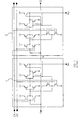
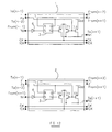
- FIG. 1 of the accompanying drawings illustrates part of a typical CMOS circuit comprising latches 1 and 2. The construction and operation of such an arrangement is well-known and will not be described in detail.
- Consecutive latches such as 1 and 2 are transparent on opposite clock phases of a two phase clock represented by CK and CK-. The input and output of each latch are "NANDed" together in order to produce the clock pulses Nn and Np as illustrated in Figure 2 of the accompanying drawings.
- Figure 2 also illustrates the two phase clock waveforms, the D input to the first latch 1, the output M of the first latch 1 which is also the input of the second latch 2, and the output Q of the second latch 2.
- a disadvantage of this arrangement is that the output pulses Nn and Np cannot be guaranteed to be non-overlapping. This can cause problems in certain applications, for example when the output pulses are used for sampling video data in pixel matrix display drivers.
- pass gate as used herein is defined to mean a semiconductor arrangement having a main conduction path which can be controlled to transmit or block the passage of an input signal.
- a static clock pulse generator comprising a clock input and N stages, characterised in that each ith one of the stages comprises a reset-set flip-flop having a set input for receiving a set signal from a gating circuit output of the (i-1)th stage and a reset input for receiving a reset signal from an (i+a)th stage, where a is greater than or equal to one, and a gating circuit for passing a clock pulse from the clock input to an output of the gating circuit when the flip-flop is set, where 1 ⁇ i ⁇ (N-a).
- the gating circuit may be arranged to hold the output of the gating circuit at an inactive state when the flip-flop is reset.
- the reset input of the flip-flop of each ith stage may be arranged to receive the reset signal from an output of the flip-flop of the (i+2)th stage.
- the reset input of the flip-flop of each ith stage may be arranged to receive the reset singal from the output of the gating circuit of the (i+1)th stage.
- the output of the gating circuit of each ith stage may be connectd to the set input of the flip-flop of the (i+1)th stage via a delay circuit.
- Each delay circuit may comprise a plurality of cascade-connected inverters.
- the generator may comprise a first stage comprising a reset-set flip-flop having a set input for receiving a start pulse and a reset input for receiving a reset signal from the (1+a)th stage, and a gating circuit for passing a clock pulse from the clock input to the second stage when the flip-flop is set.
- the generator may comprise an Nth stage comprising a reset-set flip-flop having a set input for receiving a set signal from the gating circuit output of the (N-1)th stage and a reset input, and a gating circuit for passing a clock pulse from the clock input to the reset inputs of the flip-flops of the Nth and (N-1)th stages.
- Each ith stage may comprise a first switching arrangement for selectively causing the flip-flop set input to receive a set signal from the gating circuit of the (i+1)th stage and the flip-flop reset input to receive a reset signal from the (i-a)th stage.
- the first stage may comprise a second switching arrangement for selectively causing the flip-flop set input to receive a set input signal from the gating circuit output of the second stage and the flip-flop reset input to receive a clock pulse from the gating circuit of the first stage.
- the Nth stage may comprise a third switching arrangement for selectively causing the flip-flop set input to receive a start pulse and the flip-flop reset input to receive a reset signal from the (1+a)th stage.
- At least some of the gating circuit outputs may constitute outputs of the generator.
- At least some of the outputs of the flip-flops may constitute outputs of the generator.
- the gating circuits may have inputs connected to the clock input.
- Each of the gating circuits may comprise a pass gate and a holding device for holding the output of the pass gate at an inactive state when the flip-flop is reset.
- Each of the pass gates may be a transmission gate comprising opposite conductivity metal-oxide-silicon field effect transistors whose source-drain paths are connected in antiparallel and whose gates are connected to direct and complementary outputs of the flip-flop.
- the clock input may be a two phase input.
- the pass gates of consecutive stages may be connected to different clock input phases.
- the clock pulses passed by the pass gates of the stages may be of the same polarity.
- the holding device of each stage may comprise a pull-down transistor whose control electrode is connected to a or the complementary output of the flip-flop.
- the holding device of each stage may comprise a pull-up transistor whose control electrode is connected to a or the direct output of the flip-flop.
- the clock input may be a single phase clock input.
- the clock pulses passed by the pass gates of consecutive stages may be of opposite polarity.
- the holding devices of the stages may comprise alternating pull-down and pull-up transistors, the control electrode of each pull-down transistor being connected to the complementary output of the associated flip-flop and the control electrode of each pull-up transistor being connected to the direct output of the associated flip-flop.
- Each of the gating circuits may comprise a gated sense amplifier.
- Each of the gating circuits may comprise a gated level shifter.
- Each of the flip-flops may comprise: a first inverter, at least one of whose input and output constitutes an output of the flip-flop; a second controllable inverter, whose input and output are connected to the output and input, respectively, of the first inverter; and an input circuit having first and second inputs constituting inputs of the flip-flop, the input circuit being arranged to supply to the input of the first inverter a signal corresponding to the states of the first and second inputs and to control the second inverter so as to switch the output of the second inverter to a high impedance state when the first or second input receives an active signal.
- the first input may be an active high input and the second input may be an active low input.
- the input circuit may comprise: a first active device connected between a first power supply input and the input of the first inverter and having a control electrode constituting the second input; and a second active device, of opposite conduction type to the first active device, connected between a second power supply input and the input of the first inverter and having a control electrode constituting the first input.
- Each of the first and second active devices may be connected in an inverting configuration.
- the second inverter may comprise third and fourth active devices of a first conduction type connected in series between a or the first power supply input and the output of the second inverter and fifth and sixth active devices of a second conduction type opposite the first type connected in series between a or the second power supply input and the output of the second inverter, the third and fifth active devices having control electrodes connected to the input of the second inverter and the fourth and sixth active devices having control electrodes connected to first and second inputs, respectively, of the input circuit.
- the control electrode of at least one of the third and fifth active devices may be connected to the input of the second inverter via a further active device.
- the or each further active device may have a control electrode connected to the first or second power supply input.
- the first inverter may comprise a seventh active device connected between a or the first power supply input and the output of the first inverter and an eighth active device, of opposite conduction type to the seventh active device, connected between a or the second power supply input and the output of the first inverter, the seventh and eighth active devices having control electrodes connected to the input of the first inverter.
- the generator may comprise a CMOS integrated circuit.
- a spatial light modulator comprising a generator according to the first aspect of the invention.
- the modulator may comprise a liquid crystal device.
- a display comprising a modulator according to the second aspect of the invention.
- clock pulse generator having a very high maximum frequency of operation.
- the clock pulses are required to charge only two transistor gates at a time (in addition to any external load when the gating circuit outputs constitute the outputs of the generator).
- the clock signal can be fully gated. This is important for two reasons. Firstly, transistor loading of the clock signal limits its rise and fall times and hence the maximum frequency. With the present arrangement, loading of the clock is mainly due to parasitic elements so that high speed can be maintained for relatively large clock pulse generators.
- the capacitive loading of the clock signal by transistor gates can be minimised.
- only the gates of transistors in stages which are in their switching state are charged. This results in reduced power dissipation in the track resistance of circuit tracks carrying the clock signal.
- the output pulses may be exact copies of the clock signal (degraded only by passage through the gating circuits).
- the gating circuits may be embodied as pass gates, which may be made relatively large so that the drive capability is high. The output pulses when taken from the pass gates are guaranteed to be non-overlapping.
- a variety of useful signals may be generated from each pair of consecutive stages and these include:
- the relative pulse widths may be changed merely by changing the mark-to-space ratio of the clock signal used to drive the clock pulse generator.
- voltage level shifting can be provided.
- the clock signal may be of lower voltage than the generator supply voltage so that a reduction in power consumption can be achieved.
- the output pulses may have amplitudes corresponding to substantially the whole supply voltage despite operating with clock signals of substantially lower amplitude.
- the generator can operate selectively in either direction ("forward" or "reverse”). This is advantageous in some applications, such as display driving in which the displayed image may need to be spatially inverted.
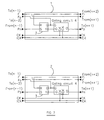
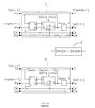
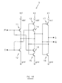
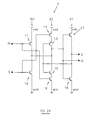
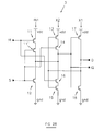
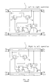
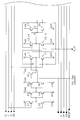
- FIG. 4 shows two stages 1 and 2 of a static clock pulse generator.
- the stage 1 comprises a reset-set (RS) flip-flop 3 having a reset input R, a set input S, a direct output Q and a complementary or inverted output !Q.
- the set input S is connected to an input of the stage for receiving a set signal Pn from the preceding or (n-1)th stage, which signal is also the output signal of the preceding stage.
- the reset input R is connected to an input Fi for receiving a reset signal from the (n+1)th stage.
- the outputs Q and !Q of the flip-flop 3 are connected to gate inputs G and !G, respectively, of a gating circuit 4, which has complementary clock inputs CK and !CK, which are connected to the complementary phases of a two phase clock input CK and !CK, respectively.
- a gating circuit 4 which has complementary clock inputs CK and !CK, which are connected to the complementary phases of a two phase clock input CK and !CK, respectively.
- the gating circuit 4 may have a single clock input connected to one of the clock phases or to a single clock phase.
- the output O of the gating circuit 4 is connected to the output Pp of the stage 1 for supplying a set signal to the following or (n+1)th stage.
- the output O of the gating circuit 4 is connected to an output Fo for supplying a reset signal to the preceding or (n-1)th stage.
- the stage 2 shown in the lower part of Figure 4 differs from the stage 1 in that the stage 2 receives a set signal Pp from the (n-1)th stage and supplies a set signal Pn to the (n+1)th stage. Also, the gating circuit 4 of the stage 1 is arranged to supply positive pulses Pp coinciding with the positive-going pulses of the clock signal CK whereas the stage 2 is arranged to supply at its output positive pulses Pn coinciding with negative-going pulses of the clock signal CK (which coincide with positive-going pulses of the complementary clock signal !CK).
- the gating circuit 4 is controlled by either or both outputs Q and !Q of the flip-flop 3 in each stage so as to transmit a single clock pulse from one of the clock inputs CK and !CK.
- the gating input signals to the circuit 4 are inactive, i.e. when the flip-flop 3 is reset, the output O of the circuit 4 and hence of the stage 1 or 2 is held low.
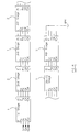
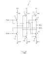
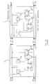
- Figure 5 shows part of a static clock pulse generator which comprises N stages 1, 2 connected in cascade.
- the stages 1 alternate with the stages 2.
- the set signal input Pn of the first stage is arranged to receive a start pulse SP whereas the clock inputs are connected to receive complementary clock signals CK and !CK from the two phase clock input.
- the input Fi of each stage 1, 2 is connected to the output Fo of the following stage.
- the input Fi of the last or Nth stage is connected to ground gnd.
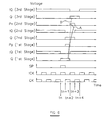
- a start pulse SP is supplied to the input Pn of the first stage 1.
- the flip-flop 3 of this stage is set so that the output Q goes high and the complementary output !Q goes low.
- the gating circuit 4 is thus switched on and the output signal Pp of the first stage follows the clock signal CK.
- the clock signal CK goes high so that the output signal Pp of the first stage 1 goes high.
- the flip-flop 3 of the second stage 2 is set so that its outputs Q and !Q go high and low, respectively.
- the gating circuit 4 of the second stage 2 is switched on so that the output signal Pn of the second stage 2 follows the complementary clock signal !CK.
- the complementary clock signal !CK goes high and hence so does the output signal Pn of the second stage 2.
- the flip-flop of the third stage 1 is thus set and its output Q goes high.
- the signal Pn is fed back to the reset input R of the flip-flop 3 of the first stage 1, which is therefore reset (as illustrated at A in Figure 6).
- the gating circuit 4 of the first stage 1 is switched off so that the output Pp of the first stage 1 remains held at ground potential until another start pulse is received.
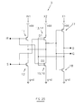
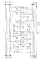
- the stages 1 and 2 shown in Figure 7 differ from those shown in Figure 4 in the feedback arrangments of resetting pulses.
- Each stage 1, 2 has an input F for receiving a reset signal from the (n+1)th stage and for routing this to an output F in order to supply the reset signal to the (n-1)th stage.
- the reset signal is supplied by the Q output of the flip-flop 3 via the output Fo to the (n-1)th stage.
- the reset input R of the flip-flop 3 connected to the input Fi receives a reset signal from the (n+2)th stage.
- the flip-flop outputs respond to the pulses generated by the gating circuits 4, the delay between each gated pulse and the response of the flip-flop is small.
- the timing of signals occurring in the clock pulse generator shown in Figure 8 and comprising the stages 1 and 2 shown in Figure 7 are therefore similar to those occurring in the clock pulse generator shown in Figure 5 so that the waveforms are almost identical to those illustrated in Figure 6.
- the rising edge of the flip-flop output Q of the third stage resets the signal Q of the first stage so that these signals are guaranteed to be overlapping. This may be an important feature if further logic signals of a certain type are required to be generated from the outputs Q of the flip-flops 3 by combinational logic.
- stages 1 and 2 shown in Figure 9 differ from those shown in Figure 4 in that the output of each stage is connected to the output O of the gating circuit 4 via a delay circuit 5, which may be embodied as an even number of series connected or cascaded inverters as shown at 5'.
- the feedback reset signal to the preceding stage is supplied directly from the output O of the gating circuit 4 via the output Fo and so is not delayed. This ensures that the flip-flop of the preceding stage is reset before the flip-flop of the succeeding stage is set.
- Figure 10 illustrates the effect of this on the outputs Q and !Q of the flip-flops of consecutive stages. This may be used by suitable combinational logic to derive further logic signals.
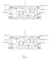
- FIG 11 shows stages 1 and 2 of the type shown in Figure 7 in which the gating circuits 4 are embodied in the form of transmission gates.
- the outputs Q and !Q of each flip-flop 3 are connected to the gates of transistors T1 and T2, respectively, whose source-drain paths are connected in antiparallal to form a transmission gate.
- the input of the transmission gate T1, T2 is connected to the phase CK or the phase !CK of the two phase clock input in the stage 1 or the stage 2, respectively.
- the output of the transmission gate T1, T2 is connected to the output Pp or Pn of the stage 1 or 2, respectively.
- a pull-down transistor T3 has a source connected to a ground or power supply input gnd, a drain connected to the output Pp of the stage 1 or Pn of the stage 2, and a gate connected to the complementary output !Q of the flip-flop 3.
- the transmission gate T1, T2 When the flip-flop 3 is in its reset state, the transmission gate T1, T2 is switched off and the transistor T3 holds the output of the stage at ground potential. When the flip-flop 3 is in its set state, the transmission gate T1, T2 is switched on to connect the stage output to the appropriate clock phase and the pull-down transistor T3 is disabled.
- stages 1 and 2 shown in Figures 4, 7, 9 and 11 supply positive pulses at the outputs Pp and Pn synchronised with the rising edges of the clock pulses CK and !CK.
- a static clock pulse generator which supplies negative output pulses Nn and Np.
- Figure 12 illustrates stages 1 and 2 which provide such pulses and which may be connected together as shown in Figure 8 to form a static clock pulse generator.
- the stage 1 shown in Figure 12 differs from that shown in Figure 11 in that an inverter 6 is connected between the input Np and the set input S of the flip-flop 3 and the output Nn is provided with a pull-up transistor T3 whose source is connected to a power supply input vdd and whose gate is connected to the direct output Q of the flip-flop 3.
- the stage 2 shown in Figure 12 differs from that shown in Figure 11 in that an inverter 6 is connected between the input Nn and the set input S of the flip-flop 3 and the output Np is provided with a pull-up transistor T3 whose gate is connected to the direct output Q of the flip-flop 3.
- FIG 13 illustrates stages 1 and 2 which may be connected together as shown in Figure 8.
- the stage 1 supplies positive going output signals Pp whereas the stage 2 supplies negative going output signals Nn.
- the stage 1 differs from that shown in Figure 11 in that an inverter 6 is provided between the input Nn and the set input S of the flip-flop 3.
- the stage 2 differs from that shown in Figure 12 in that the inverter 6 is omitted and the input of the transmission gate T1, T2 is connected to the single phase clock input CK.
- the whole static clock pulse generator requires a single phase clock input CK and alternate stages provide opposite polarity output signals or pulses.
- the flip-flops 3 may be embodied in any suitable way.
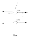
- a known type of RS flip-flop comprises a pair of cross-coupled NOR gates as shown in Figure 14 and as disclosed in F. Hill and G. Peterson, "Digital Logic and Microprocessors", John Wiley and Sons, 1984.
- the flip-flop comprises a pair of two input gates NOR1 and NOR2.
- One of the inputs of the gate NOR1 comprises a set input S whereas one of the inputs of the gate NOR2 comprises a reset input R.
- the output of the gate NOR1 comprises a complementary output !Q of the flip-flop and is connected to the second input of the gate NOR2.
- the output of the gate NOR2 comprises an output Q of the flip-flop and is connected to the second input of the gate NOR1.
- the output Q and the complementary output !Q respond to set and reset signals in accordance with the following truth table: S R Q t !Q t 0 0 Q t-1 !Q t-1 0 1 0 1 1 0 1 0 1 1 1 Undefined where 0 and 1 represent logic low and logic high levels, Q t and !Q t represent the current states of the outputs and Q t-1 and !Q t-1 represent the preceding states of the outputs.
- the set and reset signals S and R are both 0, the outputs Q and !Q retain their prior states and are thus latched.
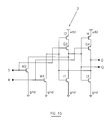
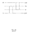
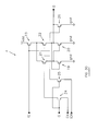
- the RS flip-flop shown in Figure 14 may be embodied as an eight transistor CMOS integrated circuit of known type as shown in Figure 15.
- the gate NOR1 comprises P-type transistors 12 and G2 and N-type transistors M2 and I1 whereas the gate NOR2 comprises P-type transistors I4 and G4 and N-type transistors M4 and I3.
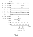
- Figure 16 of the accompanying drawings is a graph showing four waveform diagrams against a common time axis of signals occurring at the inputs R and S and at the outputs Q and !Q.
- the waveforms represent a simulation of the flip-flop illustrated in Figure 15 using arbitrary voltage levels and poor transistor performance to emphasise the relative timing of signal edges. For the purposes of the simulation, all of the transistors are of equal size and the outputs Q and !Q are each loaded with a unit inverter.
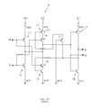
- the stages 1, 2 shown in Figure 17 differ from those shown in Figure 11 in that the flip-flop 3 has an active low reset input !R. Also, the reset signals fed back from each stage to the stage before the preceding stage are supplied by the complementary output !Q of the flip-flop 3.
- the stages 1, 2 as shown in Figure 17 allow the flip-flops 3 to be embodied by an improved type of flip-flop as shown in Figure 18.
- the flip-flop 3 comprises an input circuit IN1 comprising a first P-type transistor 11 and an N-type transistor 12 connected in series between a first power supply input or line vdd and a ground or second power supply input or line gnd.
- the first transistor 11 has a gate which is connected to an active low reset input !R.
- the reset signal supplied to the input !R is therefore normally at logic high or 1, for example at the voltage of the supply line vdd, and switches to the logic low or 0, such as zero or ground voltage, when the flip-flop is to be reset.
- the gate of the second transistor 12 is likewise connected to a set input S which is active high i.e. normally at logic low but switching to logic high when the flip-flop is to be set.
- the flip-flop further comprises a first inverter X1 and a second controllable inverter X2.
- the second inverter X2 comprises third and fourth P-type transistors 13 and 14 and fifth and sixth N-type transistors 15 and 16 connected in series between the supply lines vdd and gnd.
- the sources of the third and fifth transistors 13 and 15 are connected to the supply lines vdd and gnd, respectively whereas the gates are connected together to form the input of the inverter X2.
- the drains of the third and fifth transistors 13 and 15 are connected to the sources of the fourth and sixth transistors 14 and 16, respectively.
- the drains of the fourth and sixth transistors 14 and 16 are connected together to form the output of the second inverter X2.
- the gate of the fourth transistor 14 is connected to the set input S whereas the gate of the sixth transistor 16 is connected to the reset input !R.
- the first inverter X1 comprises a seventh P-type transistor 17 and an eighth N-type transistor 18 which are connected in series between the supply lines vdd and gnd.
- the gates of the transistors 17 and 18 are connected together to form the input of the first inverter X1 whereas the drain of the transistors 17 and 18 are connected together to form an output Q of the flip-flop.
- the input of the first inverter X1 is connected to the output of the second inverter X2 and to a complementary output !Q of the flip-flop.
- the output of the first inverter X1 is connected to the input of the second inverter X2.
- the input of the first inverter X1 is connected to the output of the input circuit IN1 formed by the drains of the transistors 11 and 12.
- the flip-flop shown in Figure 18 has an active high set input S and an active low reset input !R, its response to logic level signals differs from the arrangement illustrated in Figures 14 and 15.
- the response to the various combinations of logic level input signals is as follows: S !R Q t !Q t 0 1 Q t-1 !Q t-1 0 0 0 1 1 1 1 0 1 0 Undefined where the symbols are as described hereinbefore.
- the set signal is inactive (logic 0) and the reset signal is inactive (logic 1)
- the transistors 11 and 12 are switched off whereas the transistors 14 and 16 are conductive.
- the inverter X2 therefore functions as an inverter such that the signal at its output is the logical complement of the signal at its input.
- the flip-flop therefore comprises cross-coupled inverters with the outputs Q and !Q locked in opposite logic states which depend on whether the flip-flop was more recently set or reset.
- the flip-flop may be set by applying an active set signal (logic 1) to the set input S while the reset input !R remains at logic level 1 corresponding to the inactive reset signal.
- the second transistor 12 is thus turned on whereas the fourth transistor 14 is turned off so as to isolate the output of the second inverter X2 from the first supply line vdd.
- the input of the first inverter X1, which is connected to the output of the second inverter X2 is therefore pulled low by the transistor 12 so that the output Q is set to logic 1. This is fed back to the transistor 15, which ensures that the input of the inverter X1 is held at logic 0 after the set signal has ceased and the transistor 12 is switched off.
- the transistor 13 is similarly switched off by the feedback signal.
- the flip-flop can be reset by an inactive set signal (logic 0) and an active reset signal (logic 0).
- the first transistor 11 is turned on by the active reset signal whereas the transistor 16 is turned off.
- a logic level 1 is supplied to the input of the inverter X1 which therefore supplies a logic 0 signal at the output Q. This is fed back to the input of the second inverter X2 so that the transistor 13 conducts and the transistor 15 is switched off.
- the reset signal returns to its inactive (logic 1) level, the cross-coupled inverters X1 and X2 retain the reset state.
- both transistors 11 and 12 would conduct between the supply lines vdd and gnd and the output of the input circuit IN1 would be undefined. It is therefore essential for a designer to ensure that the input signals of the flip-flop cannot both be active at the same time.
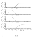
- Figure 19 illustrates input and output waveforms of the circuit of Figure 18 for set and reset operations. These waveforms were obtained by simulation using the same parameters as were used to obtain the waveforms shown in Figure 16. At time T1, the flip-flop of Figure 18 is set and the complementary output !Q responds before the output Q. similarly, at time T2, the flip-flop is reset and the complementary output !Q responds before the output Q. The flip-flop therefore provides the more desirable symmetrical switching behaviour which is advantageous in high speed logic circuits.
- Figures 20 and 21 compare the performance of the flip-flop of Figure 18 with that of the flip-flop of Figure 15 for set and reset transitions, respectively. These waveforms were obtained by simulation using the same parameters, namely equal-sized transistors of identical performance with each of the outputs driving a unit inverter load and the voltage waveforms being measured at the inputs of these inverters.
- the flip-flops are set at time T1.
- the outputs !Q of the "New RS flip-flop” of Figure 18 and of the "NOR RS flip-flop” of Figure 15 discharge at approximately the same rate.
- the speed of response of the outputs Q is substantially different.
- the output Q of the "new" flip-flop reaches the logic high state at a time T3, which is approximately 20% faster than the time taken for the output Q of the known circuit to reach the same logic level (at time T2).
- the flip-flops are reset at time T1.
- the output Q of the flip-flop of Figure 15 and the output !Q of the flip-flop of Figure 18 discharge and charge, respectively, at approximately the same rate.
- the output Q of the flip-flop of Figure 18 reaches the logic low state at time T3 substantially faster than the output !Q of the flip-flop of Figure 15 reaches the logic high state at time T2.
- Figure 22 illustrates stages 1 and 2 which differ from those shown in Figure 12 in that the inverters 6 are omitted and the flip-flops 3 have active low set inputs !S. These stages may make use of flip-flops having substantially the same architecture as illustrated in Figure 18.
- a suitable flip-flop of this type is illustrated in Figure 23, in which the inputs and outputs have been swapped.
- the gate of the first transistor 1 is connected to an active low set input !S whereas the gate of the second transistor 2 is connected to an active high reset input R.
- the output of the inverter X1 is connected to the complementary output !Q whereas the output of the inverter X2 is connected to the output Q.
- the relative position of the transistors 13 and 14 and of the transistors 15 and 16 in the second inverter is not important to the correct operation of the flip-flop.
- the transistor 14 may be disposed between the first supply line vdd and the transistor 13 and the transistor 16 may be disposed between the second supply line gnd and the transistor 15.
- pairs of transistors with their source-drain paths connected in series maybe replaced by multiple gate devices.
- the transistor 13 and 14 are replaced by a dual gate transistor D1 and the transistors 15 and 16 are replaced by a dual gate transistor D2.
- the flip-flops described hereinbefore with reference to Figures 18 and 23 to 25 are intended to operate with standard logic level signals such that the logic level 1 signal has the value of the voltage on the first power supply line vdd and the logic level 0 signal has the voltage on the second supply line gnd, these embodiments are capable operating on lower voltage input signals and may therefore perform level shifting.
- the set input S is capable of responding to an active high set signal having a voltage of Vs which is less that the supply voltage vdd (relative to the ground potential).
- the active low reset input !R of the embodiment of Figure 18 is capable of responding to a reset signal whose voltage Vr is greater than the ground potential.
- the transistor 12 can be turned on with a gate-source voltage which is less than the supply voltage.
- the transistor 14 may not be completely turned off because its gate-source voltage is equal to the difference between the supply voltage and the voltage of the set signal.
- the minimum value of the magnitude of the set signal required for the flip-flop to change state and become set may be increased by making the transistor 12 large in comparison to the transistors 13 and 14. This is the usual configuration for fast circuits with high drive capability outputs.
- the flip-flop shown in Figure 27 represents a modified version of that shown in Figure 18 and is further optimised for low input voltage operation.
- a further P-type transistor F1 arranged as a pass transistor is connected between the output of the first inverter X1 and the gate of the transistor 13.
- the gate of the transistor F1 is connected to the second supply line gnd.
- the operation of the flip-flop of Figure 27 relies on the fact that the transistor Fl can only pass a logic level 0 degraded by a threshold voltage.
- the condition of the flip-flop is such that the gate of the transistor 13 is at a potential close to the threshold voltage of the transistor F1. This ensures that the transistor 13 is only weakly turned on and that the combined pull-up drive of the transistors 13 and 14 is reduced. Consequently, during a subsequent setting operation, the flip-flop can be set with a lower input voltage Vs than could otherwise be achieved.
- an N-type transistor arranged as a pass gate is connected between the output of the inverter X1 and the gate of the transistor 15 with its gate electrode connected to the first supply line vdd.
- the flip-flop shown in Figure 28 is of a set-override type and differs from that shown in Figure 18 in that a further transistor 11' is provided.
- the transistor 11' is of P-type and is connected in series with the transistor 11.
- the drain of the transistor 11 is connected to the source of the transistor 11', the drain of the transistor 11' is connected to the drain of the transistor 12 and the gate of the transistor 11' is connected to the set input S.
- the source-drain path of the transistor 11' may be connected between the source of the transistor 11 and the supply line vdd or the transistors 11 and 11' may be embodied as a dual gate transistor.
- the operation of the flip-flop shown in Figure 28 is similar to that shown in Figure 18 but differs mainly in that there is no undefined state.
- the truth table for the flip-flop of Figure 28 is as follows: S !R Q t !Q t 0 1 Q t-1 !Q t-1 0 0 0 1 1 1 1 0 1 0 1 0 1 0 1 0 1 0
- the flip-flop of Figure 18 has an undefined state when the set and reset inputs are both simultaneously active.
- the flip-flop of 28 is arranged to be set when the set and reset inputs are both simultaneously active.
- the set input S overrides the reset input !R in this situation as illustrated in the truth table.
- the transistor 11' is turned off and disconnects the drain of the transistor 11 from the drain of the transistor 12 so that the flip-flop is forced into the set state.
- FIG 29 illustrates modified stages 1 and 2 which employ an alternative technique for providing low voltage operation. This technique may be used with single phase or two phase clock signals of amplitudes substantially lower than the power supply voltage.
- the stages 1 and 2 shown in Figure 29 differ from those shown in Figure 4 in that each of the gating circuits 4 is embodied as a gated level-shifter or gated sense amplifier. Thus, the gating circuits performs voltage level-shifting of the clock pulses.
- Figure 30 illustrates in more detail a gated sense amplifier which may be used as the gating circuit 4.
- the amplifier comprises ninth and tenth N-type transistors 19 and 20 and eleventh to thirteenth P-type transistors 21 to 23 arranged as a cross-coupled sense amplifier, for instance of the type disclosed in A. Bellaouar and M. Elmasry, "low-power digital VLSI design circuits and systems", Kluwer Academic Publishers, 1995, the contents of which are incorporated herein by reference.
- the sources of the transistors 19 and 20 are connected to ground whereas the drains thereof are connected to the drains of the transistors 21 and 22 and to the gates of the transistors 20 and 19, respectively.
- the sources of the transistors 21 and 22 are connected to the drain of the transistor 23 whose source is connected to the supply input vdd.
- the gate of the transistor 23 is connected to the complementary gate input !G.
- the amplifier further comprises fourteenth to sixteenth N-type transistors 24 to 26.
- the sources of the transistors 24 and 25 are connected to the direct and complementary clock inputs CK and !CK whereas the gates thereof arc connected together to the gate input G.
- the drains of the transistors 24 and 25 are connected to the gates of the transistors 21 and 22, respectively.
- the source-drain path of the transistor 26 is connected between the output O and ground gnd whereas the gate thereof is connected to the complementary gate input !G.
- the transistors 24 and 25 pass the clock signals to the gates of the transistors 21 and 22.
- the transistor 23 is grounded such that the sense amplifier operates with a high tail current.
- the transistor 26 is switched off so that the output O follows the logic state of the clock input CK with an appropriate level shift.
- the amplifier is disabled when the signals G and !G are low and high, respectively, so that the transistors 24 and 25 isolate the clock inputs.
- the transistor 23 is turned off so as to stop current flow through the amplifier.
- the pull-down transistor 26 is turned on so that the output O is held at its default logic low state.
- Figure 31 illustrates a gated level shifter which may be used as the gating circuit 4.
- the level shifter comprises seventeenth to nineteenth P-type transistors 27 to 29 and a twentieth N-type transistor 30.
- the sources of the transistors 27 and 29 are connected to the power supply input vdd.
- the gate of the transistor 27 is connected to the complementary gate input !G whereas the drain thereof is connected to the source of the transistor 28.
- the drain of the transistor 28 is connected to ground.
- the drain of the transistor 29 is connected to the drain of the transistor 30, whose source is connected to the complementary clock input !CK and whose gate is connected to the source of the transistor 28.
- the drains of the transistors 29 and 30 are connected to the gate of a twenty first P-type transistor 31 and a twenty second N-type transistor 32.
- the sources of the transistors 31 and 32 are connected to the power supply inputs vdd and gnd, respectively, whereas the drains thereof are connected together and to the output O.
- a twenty third N-type transistor 33 has a drain connected to the gates of the transistors 28 and 29, a source connected to the clock input CK and a gate connected to the gate input G.
- Twenty fourth and twenty fifth N-type transistors 34 and 35 have gates connected to the complementary gate input !G, sources connected to ground gnd, and drains connected to the gates of the transistors 30 and 29, respectively.
- the transistor 33 passes the clock signals to the gates of the transistors 29 and 30.
- the transistors 27 and 28 operate as a source follower with the transistor 27 switched hard on so as to provide maximum boost to the input signal.
- the transistors 34 and 35 are switched off and the circuit operates as a differential input level shifter so that the output O follows the logic state of the clock phase CK.
- the transistors 34 and 35 are turned on so as to ensure that the transistor 30 is turned off, the transistor 29 is turned on and the output of the inverter formed by the transistors 31 and 32 is held low.
- the transistor 33 isolates the clock phase CK.
- clock phases CK and !CK do not drive transistor gates directly but instead are gated by the transistors 24, 25, 30 and 33 which act as pass gates.
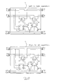
- Figure 32 illustrates a stage 1 of the type shown in Figure 11 modified for bi-directional operation.
- the upper part of Figure 32 illustrates the configuration for generating pulses in sequence from left to right whereas the lower part of Figure 32 illustrates the configuration for generating pulses in sequence from right to left. Similar modifications may be made in the other types of stages described hereinbefore.
- the modification comprises providing electronic switches 7 and 8, for instance in the form of transmission gates, for controlling the directions in which set and reset pulses are passed from stage to stage.
- the stage 1 has left and right feed back connections Fo which are selectively connected to the output Q of the flip-flop by the switch 7.
- the stage has left and right outputs Pp for set pulses supplied from the output of the transmission gate T1, T2 in accordance with the position of the switch 8.
- the switch 7 directs reset pulses from the output Q of the flip-flop to the left and via the preceding stage to the stage before the preceding stage where such pulses are used to reset the flip-flop.
- the output pulses from the transmission gate T1, T2 are supplied to the succeeding stage for setting the flip-flop thereof.
- Figure 33 illustrates a bi-directional stage 1 similar to that shown in Figure 32 but modified so as to reduce the number of signals which have to be routed between stages.
- the stage of Figure 33 differs from that of Figure 32 in that the left and right feedback connections Fo are selectively connected by the switch 7 to the output of the transmission gate comprising the transistors T1 and T2. This allows the two signal paths F of the stages shown in Figure 32 to be omitted.
- Figure 34 illustrates another bi-directional stage 1 in which the signal routing between stages is reduced even further.
- the set input S is selectively connected via the switch 7 to receive a pulse Pn from a preceding or succeeding stage whereas the reset input R of the flip-flop 3 is selectively connected via the switch 8 to receive a pulse Pn from a succeeding or preceding stage, respectively.
- Figure 35 illustrates the penultimate right hand stage 2 connected to a final stage 100 of a clock signal generator.
- the clock pulse transmitted by the final stage 100 resets that stage and also the penultimate stage.
- the switches 7 and 8 are changed over so that the flip-flop 3 of the final stage 100 is set by a start pulse SP.
- the clock pulse transmitted by this stage sets the flip-flop 3 of the penultimate stage 2 and the subsequent clock pulse passed by the penultimate stage 2 sets the flip-flop of the antepenultimate or preceding stage (1) (now shown) and resets the flip-flop of the final stage 100.
- the final stage 100 may be used in place of a pair of stages 1, 2, whose complexity is not needed.
- the stage 100 may also be used as the first stage of a bi-directional static clock pulse generator.
- the first and last stages may be of the type shown at 100 in Figure 35 but with the switches 7 and 8 replaced by the appropriate hard-wiring according to whether the stage is to be used as the first stage or the last stage of the generator.
- Figure 36 illustrates a bi-directional stage of the type shown in Figure 32 but rearranged slightly for use with flip-flops 3 of the type shown in Figure 25.
- the switch 7 is embodied by two transmission gates formed by transistors B 1 to B4 whereas the switch 8 is embodied by transmission gates formed by transistors B5 to B8.
- the direction of operation is controlled by direction control signals on lines L and !L.
- the output of the stage is indicated at S_O.
- the transistors B1, B2, B7 and B8 are turned on and the transistors B3, B4, B5 and B6 are turned off for operation from left to right. Conversely, the transistors B3, B4, B5 and B6 are turned on and the transistors B1, B2, B7 and B8 are turned off for operation from right to left.
- the transmission gates B5, B6 and B7, B8 supply the clock pulse output to output terminals QR and QL, respectively, depending on the direction of operation.
- the transmission gates B1, B2 and B3, B4 pass the signal from the complementary output !Q to the stage two places to the left or right, respectively, in order to reset the flip-flop thereof at the appropriate time.
- a reset transistor R1 is connected between a supply line vdd and the drains of the transistors 11 and 12 and has a gate connected to a reset line RESET. This arrangement ensures that all of the flip-flops of the stages are reset in response to a single signal, for instance when power is supplied to the generator.
- the various inputs and outputs D, FRL, F, FLR, FL and FR provide routing between stages for the various signals.
- the stage 1 shown in Figure 36 is of the type which provides positive output pulses Pp synchronised with the rising edge of the clock signals CK.
- a stage 2 for providing positive output pulses Pn synchronised with the rising edge of the complementary clock signal !CK differs from the stage shown in Figure 36 in that the input of the transmission gate T1, T2 is connected to the complementary clock line !CK.
- Figure 37 illustrates a static clock pulse generator comprising stages of this type arranged in cascade. This drawing illustrates the interconnections between consecutive stages.
- a start pulse SPL for operation from left to right
- a start pulse SPR is required for the Nth stage for operation from right to left.
- Direction control lines L and !L receive complementary signals for determining whether operation is from left to right or from right to left.
- a common reset line receives a common reset signal RESET for resetting the flip-flops 3 of all of the stages before commencing operation.
- stages of the type shown in Figure 36 are operated with low voltage clock inputs, several of the transistors are redundant and may be omitted.
- the P-type device T2 is superfluous and the N-type device T1 can easily pass the lower voltage signal. If the clock signals swing between gnd and vdd supply lines, the device T1 can only pass a logic high state degraded by its threshold voltage to the transistors 11 and 12 of the succeding stage. However, because the flip-flop devices can be optimised, the flip-flop may still be set with such a signal. If the transistor T2 is omitted, the P-type devices B5 and B7 are not required.
- the feedback signal passed by the transmission gates B1, B2 and B3, B4 is a negative going pulse. All transistors may not be needed because the P-type devices B1 and B3 can pass the logic low signal, possibly with acceptable degradation, sufficiently well to force resetting of the flip-flop.
- Figure 38 shows in more detail a stage similar to that shown in Figure 34 and using a flip-flop similar to that shown in Figure 28.
- the flip-flop of Figure 38 differs from that of Figure 28 in that it has an active high reset input R and an active low set input !S.
- An inverter comprising transistors 50 and 51 is connected between the active low set input and the switch 7 comprising transistors B1, B2, B5 and B6 so as to allow the flip-flop to be used in the configuration shown in Figure 34, which requires a flip-flop with active high inputs R and S.
- the switch 8 comprises transistors B3, B4, B7 and B8.
- the flip-flop shown in Figure 38 differs from that shown in Figure 28 in that the transistors 13 to 16 are replaced by dual gate transistors D1 and D2. Also, the transistor 11' is omitted and the transistor 12 is replaced by a dual gate transistor 12' whose gates are connected to the inputs R and !S.
- the flip-flop thus functions as a set-override reset-set flip-flop with an active high reset input R and an active low set input !S.
- FIGs 39a and 39b illustrate another type of bi-directional stage for a static clock pulse generator.
- This stage comprises a flip-flop formed by transistors 11 to 18 as shown in Figure 25 and a gated level shifter formed by transistors 27 to 35 as shown in Figure 31.
- the transmission gate transistors B1 to B8 correspond to and perform the same functions as the transistors Bl to B8 shown in Figure 36.
- Transistors D1 to D6 form a delay circuit of the type illustrated in at 5 in Figure 9 so as to ensure that the outputs S_O of every other stage do not overlap.
- a reset transistor R1 as shown in Figure 36 is also provided.
- This stage is shown as providing output signals S_O and S_O2, either or both of which may be used depending on the circuit application.
- the stage illustrated in Figures 39a and 39b provides positive pulses Pp synchronised with the positive-going pulses of the clock signal CK.
- Pn coinciding with the negative-going pulses of the clock signal CK
- the static clock pulse generator may be embodied as or as part of a CMOS integrated circuit.
- CMOS complementary metal-oxide-semiconductor
- LSI large scale integration
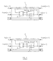
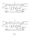
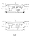
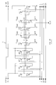
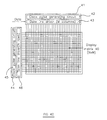
- Figure 40 illustrates a display comprising a display matrix 40 of N rows by M columns of pixels, for instance in the form of a spatial light modulator comprising a liquid crystal device.
- the display further comprises an address signal generator 41 comprising a clock pulse generating circuit 42 and a set of data line drivers 43.
- the clock pulse generating circuit 42 comprises a generator of any of the types described hereinbefore and illustrated in Figures 4 to 39b.
- a scan signal generator 44 supplies scan signals to the rows of pixels and comprises a clock pulse generating circuit 45 and a set of scan line drivers 46.
- the clock pulse generating circuit 45 comprises a generator of any of the types described hereinbefore and illustrated in Figures 4 to 39b.
- the clock pulse generating circuits generate clock pulses at pixel data rate for the circuit 42 and at line data rate for the circuit 45.
Landscapes
- Engineering & Computer Science (AREA)
- Physics & Mathematics (AREA)
- Computer Hardware Design (AREA)
- General Physics & Mathematics (AREA)
- Theoretical Computer Science (AREA)
- Chemical & Material Sciences (AREA)
- Crystallography & Structural Chemistry (AREA)
- Nonlinear Science (AREA)
- Shift Register Type Memory (AREA)
- Manipulation Of Pulses (AREA)
- Liquid Crystal Display Device Control (AREA)
- Control Of Indicators Other Than Cathode Ray Tubes (AREA)
Applications Claiming Priority (2)
| Application Number | Priority Date | Filing Date | Title |
|---|---|---|---|
| GB9828510A GB2345207A (en) | 1998-12-22 | 1998-12-22 | Static clock pulse generator for LCD |
| GB9828510 | 1998-12-22 |
Publications (1)
| Publication Number | Publication Date |
|---|---|
| EP1017060A1 true EP1017060A1 (en) | 2000-07-05 |
Family
ID=10844943
Family Applications (1)
| Application Number | Title | Priority Date | Filing Date |
|---|---|---|---|
| EP99310422A Withdrawn EP1017060A1 (en) | 1998-12-22 | 1999-12-22 | Static clock pulse generator, spatial light modulator and display. |
Country Status (5)
| Country | Link |
|---|---|
| US (1) | US6377099B1 (enExample) |
| EP (1) | EP1017060A1 (enExample) |
| JP (1) | JP3552972B2 (enExample) |
| KR (1) | KR100315610B1 (enExample) |
| GB (1) | GB2345207A (enExample) |
Cited By (4)
| Publication number | Priority date | Publication date | Assignee | Title |
|---|---|---|---|---|
| EP1492078A3 (en) * | 2003-06-23 | 2006-05-17 | Samsung Electronics Co., Ltd. | Display driving device with partitioned gate driving unit and liquid crystal display apparatus and method using the same |
| CN100362593C (zh) * | 2003-01-25 | 2008-01-16 | 夏普株式会社 | 移位寄存器 |
| CN101894517A (zh) * | 2009-05-21 | 2010-11-24 | 株式会社半导体能源研究所 | 电子电路、显示装置、电子设备以及电子电路的驱动方法 |
| US8035415B2 (en) | 2004-06-14 | 2011-10-11 | Semiconductor Energy Laboratory Co., Ltd. | Shift register and semiconductor display device |
Families Citing this family (23)
| Publication number | Priority date | Publication date | Assignee | Title |
|---|---|---|---|---|
| GB2361121A (en) * | 2000-04-04 | 2001-10-10 | Sharp Kk | A CMOS LCD scan pulse generating chain comprising static latches |
| SG153651A1 (en) * | 2001-07-16 | 2009-07-29 | Semiconductor Energy Lab | Shift register and method of driving the same |
| US20050012484A1 (en) * | 2001-11-02 | 2005-01-20 | Carl Gifford | Multizone capacitive anti-pinch system |
| WO2003107314A2 (en) * | 2002-06-01 | 2003-12-24 | Samsung Electronics Co., Ltd. | Method of driving a shift register, a shift register, a liquid crystal display device having the shift register |
| US7019884B2 (en) * | 2003-03-31 | 2006-03-28 | Intel Corporation | Light modulator with bi-directional drive |
| TWI263191B (en) * | 2003-11-18 | 2006-10-01 | Ind Tech Res Inst | Shift-register circuit |
| JP4608982B2 (ja) * | 2004-01-15 | 2011-01-12 | ソニー株式会社 | パルス信号生成方法、シフト回路、および表示装置 |
| JP4741293B2 (ja) * | 2004-06-14 | 2011-08-03 | 株式会社半導体エネルギー研究所 | シフトレジスタ及び半導体表示装置 |
| US7294089B2 (en) * | 2005-08-15 | 2007-11-13 | Ford Global Technologies, Llc | Multiple-speed automatic transmission |
| GB2446187A (en) * | 2007-01-30 | 2008-08-06 | Sharp Kk | A bidirectional scan pulse generator for an active matrix LCD display |
| GB2452278A (en) * | 2007-08-30 | 2009-03-04 | Sharp Kk | A scan pulse shift register for an active matrix LCD display |
| GB2452279A (en) * | 2007-08-30 | 2009-03-04 | Sharp Kk | An LCD scan pulse shift register stage with a gate line driver and a separate logic output buffer |
| JP2009124465A (ja) * | 2007-11-15 | 2009-06-04 | Seiko Epson Corp | ノイズフィルタ回路、およびその方法、ならびに、サーマルヘッドドライバ、サーマルヘッド、電子機器、および印刷システム |
| US20090167395A1 (en) * | 2007-12-31 | 2009-07-02 | Texas Instruments Incorporated | High performance latches |
| GB2459451A (en) * | 2008-04-22 | 2009-10-28 | Sharp Kk | A scan pulse shift register for an active matrix display |
| GB2459661A (en) * | 2008-04-29 | 2009-11-04 | Sharp Kk | A low power NMOS latch for an LCD scan pulse shift register |
| CN103081360B (zh) * | 2010-09-02 | 2016-04-27 | 夏普株式会社 | 驱动电路 |
| JP5774911B2 (ja) * | 2011-06-01 | 2015-09-09 | 株式会社ジャパンディスプレイ | 表示装置 |
| KR102051389B1 (ko) * | 2013-01-11 | 2019-12-03 | 엘지디스플레이 주식회사 | 액정표시장치 및 이의 구동회로 |
| CN104269132B (zh) * | 2014-10-29 | 2016-08-03 | 京东方科技集团股份有限公司 | 一种移位寄存单元、显示面板和显示装置 |
| US9473117B2 (en) * | 2015-02-13 | 2016-10-18 | Samsung Electronics Co., Ltd. | Multi-bit flip-flops and scan chain circuits |
| CN105337590B (zh) * | 2015-10-26 | 2017-10-17 | 宁波大学 | 一种基于cnfet的双边沿脉冲信号发生器 |
| CN106710561B (zh) * | 2017-03-08 | 2019-09-17 | 京东方科技集团股份有限公司 | 一种移位寄存器、栅线集成驱动电路及显示装置 |
Citations (6)
| Publication number | Priority date | Publication date | Assignee | Title |
|---|---|---|---|---|
| US4295055A (en) * | 1978-06-12 | 1981-10-13 | Hitachi, Ltd. | Circuit for generating scanning pulses |
| US5619157A (en) * | 1993-12-14 | 1997-04-08 | Sony Corporation | Synchronizing circuit with dynamic and static latch circuitry |
| JPH09153296A (ja) * | 1995-11-30 | 1997-06-10 | Matsushita Electric Ind Co Ltd | 液晶表示装置及びそのシフトレジスタ回路 |
| US5691740A (en) * | 1987-04-03 | 1997-11-25 | Canon Kabushiki Kaisha | Liquid crystal apparatus and driving method |
| US5790626A (en) * | 1996-09-10 | 1998-08-04 | Hewlett-Packard Company | Bi-directional linear feedback shift register |
| EP0875881A2 (en) * | 1997-04-30 | 1998-11-04 | SHARP Corporation | Active matrix light modulators, use of an active matrix light modulator, and display |
Family Cites Families (3)
| Publication number | Priority date | Publication date | Assignee | Title |
|---|---|---|---|---|
| DE69317927T2 (de) * | 1992-02-28 | 1998-11-19 | Sony Corp | Halbleiterspeicheranordnung mit einer Adressübergangsabfühlschaltung |
| US5646566A (en) * | 1996-06-21 | 1997-07-08 | International Business Machines Corporation | Low power clocked set/reset fast dynamic latch |
| US5952859A (en) * | 1998-03-09 | 1999-09-14 | Sun Microsystems, Inc. | Dynamic set/reset circuit with dual feedback |
-
1998
- 1998-12-22 GB GB9828510A patent/GB2345207A/en not_active Withdrawn
-
1999
- 1999-12-16 US US09/464,155 patent/US6377099B1/en not_active Expired - Fee Related
- 1999-12-21 JP JP36290099A patent/JP3552972B2/ja not_active Expired - Lifetime
- 1999-12-22 KR KR1019990060142A patent/KR100315610B1/ko not_active Expired - Fee Related
- 1999-12-22 EP EP99310422A patent/EP1017060A1/en not_active Withdrawn
Patent Citations (6)
| Publication number | Priority date | Publication date | Assignee | Title |
|---|---|---|---|---|
| US4295055A (en) * | 1978-06-12 | 1981-10-13 | Hitachi, Ltd. | Circuit for generating scanning pulses |
| US5691740A (en) * | 1987-04-03 | 1997-11-25 | Canon Kabushiki Kaisha | Liquid crystal apparatus and driving method |
| US5619157A (en) * | 1993-12-14 | 1997-04-08 | Sony Corporation | Synchronizing circuit with dynamic and static latch circuitry |
| JPH09153296A (ja) * | 1995-11-30 | 1997-06-10 | Matsushita Electric Ind Co Ltd | 液晶表示装置及びそのシフトレジスタ回路 |
| US5790626A (en) * | 1996-09-10 | 1998-08-04 | Hewlett-Packard Company | Bi-directional linear feedback shift register |
| EP0875881A2 (en) * | 1997-04-30 | 1998-11-04 | SHARP Corporation | Active matrix light modulators, use of an active matrix light modulator, and display |
Non-Patent Citations (1)
| Title |
|---|
| PATENT ABSTRACTS OF JAPAN vol. 1997, no. 10 31 October 1997 (1997-10-31) * |
Cited By (9)
| Publication number | Priority date | Publication date | Assignee | Title |
|---|---|---|---|---|
| CN100362593C (zh) * | 2003-01-25 | 2008-01-16 | 夏普株式会社 | 移位寄存器 |
| EP1492078A3 (en) * | 2003-06-23 | 2006-05-17 | Samsung Electronics Co., Ltd. | Display driving device with partitioned gate driving unit and liquid crystal display apparatus and method using the same |
| US7385576B2 (en) | 2003-06-23 | 2008-06-10 | Samsung Electronics Co., Ltd. | Display driving device and method and liquid crystal display apparatus having the same |
| US8274460B2 (en) | 2003-06-23 | 2012-09-25 | Samsung Electronics Co., Ltd. | Display driving device and method and liquid crystal display apparatus having the same |
| US8035415B2 (en) | 2004-06-14 | 2011-10-11 | Semiconductor Energy Laboratory Co., Ltd. | Shift register and semiconductor display device |
| US8664976B2 (en) | 2004-06-14 | 2014-03-04 | Semiconductor Energy Laboratory Co., Ltd. | Shift register and semiconductor display device |
| CN101894517A (zh) * | 2009-05-21 | 2010-11-24 | 株式会社半导体能源研究所 | 电子电路、显示装置、电子设备以及电子电路的驱动方法 |
| US8872745B2 (en) | 2009-05-21 | 2014-10-28 | Semiconductor Energy Laboratory Co., Ltd. | Electronic circuit, display device, electronic device, and method for driving electronic circuit |
| CN101894517B (zh) * | 2009-05-21 | 2015-03-11 | 株式会社半导体能源研究所 | 电子电路、显示装置、电子设备以及电子电路的驱动方法 |
Also Published As
| Publication number | Publication date |
|---|---|
| KR100315610B1 (ko) | 2001-12-12 |
| JP2000236234A (ja) | 2000-08-29 |
| GB2345207A (en) | 2000-06-28 |
| GB9828510D0 (en) | 1999-02-17 |
| JP3552972B2 (ja) | 2004-08-11 |
| KR20000052545A (ko) | 2000-08-25 |
| US6377099B1 (en) | 2002-04-23 |
Similar Documents
| Publication | Publication Date | Title |
|---|---|---|
| US6377099B1 (en) | Static clock pulse generator, spatial light modulator and display | |
| US5760609A (en) | Clock signal providing circuit with enable and a pulse generator with enable for use in a block clock circuit of a programmable logic device | |
| JP4737627B2 (ja) | スタティッククロックパルス発生器およびディスプレイ | |
| US5250852A (en) | Circuitry and method for latching a logic state | |
| US8975943B2 (en) | Compact level shifter | |
| KR100514029B1 (ko) | 레벨 시프팅 회로 및 액티브 매트릭스 드라이버 | |
| JPH05276016A (ja) | ランダム論理適用のための動的レイショレス・サーキットリー | |
| US5432529A (en) | Output circuit for electronic display device driver | |
| US4736119A (en) | Dynamic CMOS current surge control | |
| US6215346B1 (en) | Clock pulse generator, spatial light modulator and display | |
| CN1728223B (zh) | 显示设备驱动电路 | |
| US6249168B1 (en) | Clock pulse generator | |
| US20050168244A1 (en) | Single stage, level restore circuit with mixed signal inputs | |
| US6630846B2 (en) | Modified charge recycling differential logic | |
| US6661257B2 (en) | Method for clocking charge recycling differential logic | |
| JP2538628B2 (ja) | 半導体集積回路 | |
| EP1622123B1 (en) | Display device driving circuit | |
| US7764100B2 (en) | DFLOP circuit for an externally asynchronous-internally clocked system | |
| GB2345206A (en) | Set-reset bistable with symmetrical delay times | |
| JPH04261217A (ja) | 演算回路 |
Legal Events
| Date | Code | Title | Description |
|---|---|---|---|
| PUAI | Public reference made under article 153(3) epc to a published international application that has entered the european phase |
Free format text: ORIGINAL CODE: 0009012 |
|
| AK | Designated contracting states |
Kind code of ref document: A1 Designated state(s): DE FR GB |
|
| AX | Request for extension of the european patent |
Free format text: AL;LT;LV;MK;RO;SI |
|
| 17P | Request for examination filed |
Effective date: 20000914 |
|
| AKX | Designation fees paid |
Free format text: DE FR GB |
|
| 17Q | First examination report despatched |
Effective date: 20041202 |
|
| STAA | Information on the status of an ep patent application or granted ep patent |
Free format text: STATUS: THE APPLICATION IS DEEMED TO BE WITHDRAWN |
|
| 18D | Application deemed to be withdrawn |
Effective date: 20051101 |