EP1016971A2 - Multiprozessor-Digitaldatenverarbeitungssystem - Google Patents
Multiprozessor-Digitaldatenverarbeitungssystem Download PDFInfo
- Publication number
- EP1016971A2 EP1016971A2 EP00200994A EP00200994A EP1016971A2 EP 1016971 A2 EP1016971 A2 EP 1016971A2 EP 00200994 A EP00200994 A EP 00200994A EP 00200994 A EP00200994 A EP 00200994A EP 1016971 A2 EP1016971 A2 EP 1016971A2
- Authority
- EP
- European Patent Office
- Prior art keywords
- memory
- page
- state
- sub
- access
- Prior art date
- Legal status (The legal status is an assumption and is not a legal conclusion. Google has not performed a legal analysis and makes no representation as to the accuracy of the status listed.)
- Withdrawn
Links
Images


Classifications
-
- G—PHYSICS
- G06—COMPUTING OR CALCULATING; COUNTING
- G06F—ELECTRIC DIGITAL DATA PROCESSING
- G06F9/00—Arrangements for program control, e.g. control units
- G06F9/06—Arrangements for program control, e.g. control units using stored programs, i.e. using an internal store of processing equipment to receive or retain programs
- G06F9/46—Multiprogramming arrangements
- G06F9/50—Allocation of resources, e.g. of the central processing unit [CPU]
- G06F9/5005—Allocation of resources, e.g. of the central processing unit [CPU] to service a request
- G06F9/5011—Allocation of resources, e.g. of the central processing unit [CPU] to service a request the resources being hardware resources other than CPUs, Servers and Terminals
- G06F9/5016—Allocation of resources, e.g. of the central processing unit [CPU] to service a request the resources being hardware resources other than CPUs, Servers and Terminals the resource being the memory
-
- G—PHYSICS
- G06—COMPUTING OR CALCULATING; COUNTING
- G06F—ELECTRIC DIGITAL DATA PROCESSING
- G06F11/00—Error detection; Error correction; Monitoring
- G06F11/004—Error avoidance
-
- G—PHYSICS
- G06—COMPUTING OR CALCULATING; COUNTING
- G06F—ELECTRIC DIGITAL DATA PROCESSING
- G06F11/00—Error detection; Error correction; Monitoring
- G06F11/07—Responding to the occurrence of a fault, e.g. fault tolerance
- G06F11/0703—Error or fault processing not based on redundancy, i.e. by taking additional measures to deal with the error or fault not making use of redundancy in operation, in hardware, or in data representation
- G06F11/0706—Error or fault processing not based on redundancy, i.e. by taking additional measures to deal with the error or fault not making use of redundancy in operation, in hardware, or in data representation the processing taking place on a specific hardware platform or in a specific software environment
- G06F11/0721—Error or fault processing not based on redundancy, i.e. by taking additional measures to deal with the error or fault not making use of redundancy in operation, in hardware, or in data representation the processing taking place on a specific hardware platform or in a specific software environment within a central processing unit [CPU]
- G06F11/0724—Error or fault processing not based on redundancy, i.e. by taking additional measures to deal with the error or fault not making use of redundancy in operation, in hardware, or in data representation the processing taking place on a specific hardware platform or in a specific software environment within a central processing unit [CPU] in a multiprocessor or a multi-core unit
-
- G—PHYSICS
- G06—COMPUTING OR CALCULATING; COUNTING
- G06F—ELECTRIC DIGITAL DATA PROCESSING
- G06F11/00—Error detection; Error correction; Monitoring
- G06F11/07—Responding to the occurrence of a fault, e.g. fault tolerance
- G06F11/0703—Error or fault processing not based on redundancy, i.e. by taking additional measures to deal with the error or fault not making use of redundancy in operation, in hardware, or in data representation
- G06F11/0706—Error or fault processing not based on redundancy, i.e. by taking additional measures to deal with the error or fault not making use of redundancy in operation, in hardware, or in data representation the processing taking place on a specific hardware platform or in a specific software environment
- G06F11/073—Error or fault processing not based on redundancy, i.e. by taking additional measures to deal with the error or fault not making use of redundancy in operation, in hardware, or in data representation the processing taking place on a specific hardware platform or in a specific software environment in a memory management context, e.g. virtual memory or cache management
-
- G—PHYSICS
- G06—COMPUTING OR CALCULATING; COUNTING
- G06F—ELECTRIC DIGITAL DATA PROCESSING
- G06F11/00—Error detection; Error correction; Monitoring
- G06F11/07—Responding to the occurrence of a fault, e.g. fault tolerance
- G06F11/0703—Error or fault processing not based on redundancy, i.e. by taking additional measures to deal with the error or fault not making use of redundancy in operation, in hardware, or in data representation
- G06F11/0766—Error or fault reporting or storing
- G06F11/0772—Means for error signaling, e.g. using interrupts, exception flags, dedicated error registers
-
- G—PHYSICS
- G06—COMPUTING OR CALCULATING; COUNTING
- G06F—ELECTRIC DIGITAL DATA PROCESSING
- G06F12/00—Accessing, addressing or allocating within memory systems or architectures
- G06F12/02—Addressing or allocation; Relocation
- G06F12/08—Addressing or allocation; Relocation in hierarchically structured memory systems, e.g. virtual memory systems
- G06F12/0802—Addressing of a memory level in which the access to the desired data or data block requires associative addressing means, e.g. caches
- G06F12/0806—Multiuser, multiprocessor or multiprocessing cache systems
- G06F12/0811—Multiuser, multiprocessor or multiprocessing cache systems with multilevel cache hierarchies
-
- G—PHYSICS
- G06—COMPUTING OR CALCULATING; COUNTING
- G06F—ELECTRIC DIGITAL DATA PROCESSING
- G06F12/00—Accessing, addressing or allocating within memory systems or architectures
- G06F12/02—Addressing or allocation; Relocation
- G06F12/08—Addressing or allocation; Relocation in hierarchically structured memory systems, e.g. virtual memory systems
- G06F12/0802—Addressing of a memory level in which the access to the desired data or data block requires associative addressing means, e.g. caches
- G06F12/0806—Multiuser, multiprocessor or multiprocessing cache systems
- G06F12/0813—Multiuser, multiprocessor or multiprocessing cache systems with a network or matrix configuration
-
- G—PHYSICS
- G06—COMPUTING OR CALCULATING; COUNTING
- G06F—ELECTRIC DIGITAL DATA PROCESSING
- G06F12/00—Accessing, addressing or allocating within memory systems or architectures
- G06F12/02—Addressing or allocation; Relocation
- G06F12/08—Addressing or allocation; Relocation in hierarchically structured memory systems, e.g. virtual memory systems
- G06F12/0802—Addressing of a memory level in which the access to the desired data or data block requires associative addressing means, e.g. caches
- G06F12/0806—Multiuser, multiprocessor or multiprocessing cache systems
- G06F12/0815—Cache consistency protocols
- G06F12/0817—Cache consistency protocols using directory methods
-
- G—PHYSICS
- G06—COMPUTING OR CALCULATING; COUNTING
- G06F—ELECTRIC DIGITAL DATA PROCESSING
- G06F12/00—Accessing, addressing or allocating within memory systems or architectures
- G06F12/02—Addressing or allocation; Relocation
- G06F12/08—Addressing or allocation; Relocation in hierarchically structured memory systems, e.g. virtual memory systems
- G06F12/0802—Addressing of a memory level in which the access to the desired data or data block requires associative addressing means, e.g. caches
- G06F12/0806—Multiuser, multiprocessor or multiprocessing cache systems
- G06F12/0815—Cache consistency protocols
- G06F12/0831—Cache consistency protocols using a bus scheme, e.g. with bus monitoring or watching means
- G06F12/0833—Cache consistency protocols using a bus scheme, e.g. with bus monitoring or watching means in combination with broadcast means (e.g. for invalidation or updating)
-
- G—PHYSICS
- G06—COMPUTING OR CALCULATING; COUNTING
- G06F—ELECTRIC DIGITAL DATA PROCESSING
- G06F12/00—Accessing, addressing or allocating within memory systems or architectures
- G06F12/02—Addressing or allocation; Relocation
- G06F12/08—Addressing or allocation; Relocation in hierarchically structured memory systems, e.g. virtual memory systems
- G06F12/10—Address translation
- G06F12/1009—Address translation using page tables, e.g. page table structures
- G06F12/1018—Address translation using page tables, e.g. page table structures involving hashing techniques, e.g. inverted page tables
-
- G—PHYSICS
- G06—COMPUTING OR CALCULATING; COUNTING
- G06F—ELECTRIC DIGITAL DATA PROCESSING
- G06F9/00—Arrangements for program control, e.g. control units
- G06F9/06—Arrangements for program control, e.g. control units using stored programs, i.e. using an internal store of processing equipment to receive or retain programs
- G06F9/30—Arrangements for executing machine instructions, e.g. instruction decode
- G06F9/30003—Arrangements for executing specific machine instructions
- G06F9/3004—Arrangements for executing specific machine instructions to perform operations on memory
- G06F9/30047—Prefetch instructions; cache control instructions
-
- G—PHYSICS
- G06—COMPUTING OR CALCULATING; COUNTING
- G06F—ELECTRIC DIGITAL DATA PROCESSING
- G06F9/00—Arrangements for program control, e.g. control units
- G06F9/06—Arrangements for program control, e.g. control units using stored programs, i.e. using an internal store of processing equipment to receive or retain programs
- G06F9/30—Arrangements for executing machine instructions, e.g. instruction decode
- G06F9/30003—Arrangements for executing specific machine instructions
- G06F9/30076—Arrangements for executing specific machine instructions to perform miscellaneous control operations, e.g. NOP
- G06F9/30087—Synchronisation or serialisation instructions
-
- G—PHYSICS
- G06—COMPUTING OR CALCULATING; COUNTING
- G06F—ELECTRIC DIGITAL DATA PROCESSING
- G06F9/00—Arrangements for program control, e.g. control units
- G06F9/06—Arrangements for program control, e.g. control units using stored programs, i.e. using an internal store of processing equipment to receive or retain programs
- G06F9/30—Arrangements for executing machine instructions, e.g. instruction decode
- G06F9/32—Address formation of the next instruction, e.g. by incrementing the instruction counter
- G06F9/322—Address formation of the next instruction, e.g. by incrementing the instruction counter for non-sequential address
- G06F9/323—Address formation of the next instruction, e.g. by incrementing the instruction counter for non-sequential address for indirect branch instructions
-
- G—PHYSICS
- G06—COMPUTING OR CALCULATING; COUNTING
- G06F—ELECTRIC DIGITAL DATA PROCESSING
- G06F9/00—Arrangements for program control, e.g. control units
- G06F9/06—Arrangements for program control, e.g. control units using stored programs, i.e. using an internal store of processing equipment to receive or retain programs
- G06F9/30—Arrangements for executing machine instructions, e.g. instruction decode
- G06F9/38—Concurrent instruction execution, e.g. pipeline or look ahead
- G06F9/3824—Operand accessing
- G06F9/383—Operand prefetching
-
- G—PHYSICS
- G06—COMPUTING OR CALCULATING; COUNTING
- G06F—ELECTRIC DIGITAL DATA PROCESSING
- G06F9/00—Arrangements for program control, e.g. control units
- G06F9/06—Arrangements for program control, e.g. control units using stored programs, i.e. using an internal store of processing equipment to receive or retain programs
- G06F9/30—Arrangements for executing machine instructions, e.g. instruction decode
- G06F9/38—Concurrent instruction execution, e.g. pipeline or look ahead
- G06F9/3836—Instruction issuing, e.g. dynamic instruction scheduling or out of order instruction execution
- G06F9/3851—Instruction issuing, e.g. dynamic instruction scheduling or out of order instruction execution from multiple instruction streams, e.g. multistreaming
-
- G—PHYSICS
- G06—COMPUTING OR CALCULATING; COUNTING
- G06F—ELECTRIC DIGITAL DATA PROCESSING
- G06F9/00—Arrangements for program control, e.g. control units
- G06F9/06—Arrangements for program control, e.g. control units using stored programs, i.e. using an internal store of processing equipment to receive or retain programs
- G06F9/30—Arrangements for executing machine instructions, e.g. instruction decode
- G06F9/38—Concurrent instruction execution, e.g. pipeline or look ahead
- G06F9/3854—Instruction completion, e.g. retiring, committing or graduating
- G06F9/3856—Reordering of instructions, e.g. using queues or age tags
-
- G—PHYSICS
- G06—COMPUTING OR CALCULATING; COUNTING
- G06F—ELECTRIC DIGITAL DATA PROCESSING
- G06F9/00—Arrangements for program control, e.g. control units
- G06F9/06—Arrangements for program control, e.g. control units using stored programs, i.e. using an internal store of processing equipment to receive or retain programs
- G06F9/30—Arrangements for executing machine instructions, e.g. instruction decode
- G06F9/38—Concurrent instruction execution, e.g. pipeline or look ahead
- G06F9/3854—Instruction completion, e.g. retiring, committing or graduating
- G06F9/3858—Result writeback, i.e. updating the architectural state or memory
-
- G—PHYSICS
- G06—COMPUTING OR CALCULATING; COUNTING
- G06F—ELECTRIC DIGITAL DATA PROCESSING
- G06F9/00—Arrangements for program control, e.g. control units
- G06F9/06—Arrangements for program control, e.g. control units using stored programs, i.e. using an internal store of processing equipment to receive or retain programs
- G06F9/30—Arrangements for executing machine instructions, e.g. instruction decode
- G06F9/38—Concurrent instruction execution, e.g. pipeline or look ahead
- G06F9/3861—Recovery, e.g. branch miss-prediction, exception handling
- G06F9/3865—Recovery, e.g. branch miss-prediction, exception handling using deferred exception handling, e.g. exception flags
-
- G—PHYSICS
- G06—COMPUTING OR CALCULATING; COUNTING
- G06F—ELECTRIC DIGITAL DATA PROCESSING
- G06F9/00—Arrangements for program control, e.g. control units
- G06F9/06—Arrangements for program control, e.g. control units using stored programs, i.e. using an internal store of processing equipment to receive or retain programs
- G06F9/46—Multiprogramming arrangements
- G06F9/468—Specific access rights for resources, e.g. using capability register
-
- G—PHYSICS
- G06—COMPUTING OR CALCULATING; COUNTING
- G06F—ELECTRIC DIGITAL DATA PROCESSING
- G06F9/00—Arrangements for program control, e.g. control units
- G06F9/06—Arrangements for program control, e.g. control units using stored programs, i.e. using an internal store of processing equipment to receive or retain programs
- G06F9/46—Multiprogramming arrangements
- G06F9/52—Program synchronisation; Mutual exclusion, e.g. by means of semaphores
-
- H—ELECTRICITY
- H04—ELECTRIC COMMUNICATION TECHNIQUE
- H04L—TRANSMISSION OF DIGITAL INFORMATION, e.g. TELEGRAPHIC COMMUNICATION
- H04L12/00—Data switching networks
- H04L12/28—Data switching networks characterised by path configuration, e.g. LAN [Local Area Networks] or WAN [Wide Area Networks]
- H04L12/46—Interconnection of networks
- H04L12/4637—Interconnected ring systems
-
- H—ELECTRICITY
- H04—ELECTRIC COMMUNICATION TECHNIQUE
- H04L—TRANSMISSION OF DIGITAL INFORMATION, e.g. TELEGRAPHIC COMMUNICATION
- H04L45/00—Routing or path finding of packets in data switching networks
- H04L45/02—Topology update or discovery
- H04L45/04—Interdomain routing, e.g. hierarchical routing
-
- G—PHYSICS
- G06—COMPUTING OR CALCULATING; COUNTING
- G06F—ELECTRIC DIGITAL DATA PROCESSING
- G06F12/00—Accessing, addressing or allocating within memory systems or architectures
- G06F12/02—Addressing or allocation; Relocation
- G06F12/08—Addressing or allocation; Relocation in hierarchically structured memory systems, e.g. virtual memory systems
- G06F12/12—Replacement control
- G06F12/121—Replacement control using replacement algorithms
- G06F12/126—Replacement control using replacement algorithms with special data handling, e.g. priority of data or instructions, handling errors or pinning
-
- G—PHYSICS
- G06—COMPUTING OR CALCULATING; COUNTING
- G06F—ELECTRIC DIGITAL DATA PROCESSING
- G06F2212/00—Indexing scheme relating to accessing, addressing or allocation within memory systems or architectures
- G06F2212/27—Using a specific cache architecture
- G06F2212/272—Cache only memory architecture [COMA]
Definitions
- This invention relates to digital data processing systems and, more particularly, to multiprocessing systems with distributed hierarchical memory architectures.
- the art provides a number of configurations for coupling the processing units of multiprocessing systems.
- processing units that shared data stored in system memory banks were coupled to those banks via high-bandwidth shared buses or switching networks.
- bottlenecks were likely to develop as multiple processing units simultaneously contended for access to the shared data.
- Wilson Jr. et al United Kingdom Patent Application No. 2,178,205, wherein a multiprocessing system is said to include distributed cache memory elements coupled with one another over a first bus.
- a second, higher level cache memory attached to the first bus and to either a still higher level cache or to the main system memory, retains copies of every memory location in the caches below it.
- the still higher level caches, if any, and system main memory in turn, retain copies of each memory location of cache below them.
- the Wilson Jr. et al processors are understood to transmit modified copies of data from their own dedicated caches to associated higher level caches and to the system main memory, while concurrently signalling other caches to invalidate their own copies of that newly-modified data.
- a further object is to provide a multiprocessing system with unlimited scalability.
- Another objects of the invention are to provide a physically distributed memory multiprocessing system which requires little or no software overhead to maintain data coherency, as well as to provide a multiprocessing system with increased bus bandwidth and improved synchronization.
- a digital data processing system comprising a plurality of processing cells arranged in a hierarchy of rings.
- the system selectively allocates storage and moves exclusive data copies from cell to cell in response to access requests generated by the cells. Routing elements are employed to selectively broadcast data access requests, updates and transfers on the rings.
- a system of the type provided by the invention does not require a main memory element, i.e., a memory element coupled to and shared by the systems many processors. Rather, data maintained by the system is distributed, both on exclusive and shared bases, among the memory elements associated with those processors. Modifications to datum stored exclusively in any one processing cell do not have to be communicated along the bus structure to other storage areas. As a result of this design, only that data which the processors dynamically share, e.g., sharing required by the executing program themselves, must be transmitted along the bus structure.
- the processing cells include central processing units coupled with memory elements, each including a physical data and control signal store, a directory, and a control element.
- Groups of cells are interconnected along unidirectional intercellular bus rings, forming units referred to as segments. These segments together form a larger unit referred to as "information transfer domain(0).” While cells residing within each segment may communicate directly with one another via the associated intercellular bus, the associated central processing units are not themselves interconnected. Rather, intersegment communications are carried out via the exchange of data and control signals stored in the memory elements.
- a memory management element facilitates this transfer of information.
- Communications between cells of different domain(0) segments are carried out on higher level information transfer domains.
- These higher level domains are made up of one or more segments, each comprising a plurality of domain routing elements coupled via a unidirectional bus ring. It will be appreciated that the segments of higher level domains differ from those of domain(0) insofar as the former comprise a ring of routing elements, while the latter comprise a ring of processing cells.
- Each routing element is connected with an associated one of the segments of the next lower information transfer domain. These connected lower segments are referred to as "descendants.” Every information transfer domain includes fewer segments than the next lower domain. Apart from the single segment of the system's highest level domain, signals are transferred between segments of each information transfer domain via segments of the next higher domain.
- An exemplary system having six domain(0) segments includes two domain(1) segments, the first which transfers data between a first three of the domain(0) segments, and the second of which transfers data between the other three domain(0) segments, Data is transferred between the two domain(1) segments over a domain(2) segment having two domain routing elements, each connected with a corresponding one of the domain(1) segments.
- the system's memory elements each include a directory element that maintains a list of descriptors reflecting the identity and state of each datum stored in the corresponding memory.
- One portion of each descriptor is derived from the associated datum's system address, while another portion represents an access state governing the manner in which the local central processing unit may utilize the datum.
- This access state may include any one of an "ownership" state, a read-only state, and an invalid state.
- the first of these states is associated with data which can be modified by the local central processing unit, i.e., that unit included within the cell in which the datum is stored.
- the read-only state is associated with data which may be read, but not modified, by the local central processing unit.
- the invalid state is associated with invalid data copies.
- the domain routing elements themselves maintain directories listing all descriptors stored in their descendant domain(0) segments.
- the routing elements of first domain(1) segments maintain directories reflecting the combined content of the cells of their respective domain(0) segment.
- the single routing element of the domain(2) segment maintains a directory listing all descriptors retained in all of the system's processing cells.
- Data access requests generated by a processor are handled by the local memory element whenever possible. More particularly, a controller coupled with each memory monitors the cell's internal bus and responds to local processor requests by comparing the request with descriptors listed in the corresponding directory. If found, matching data is transmitted back along the internal bus to the requesting processor.
- Data requests that cannot be resolved locally are passed from the processing cell to the memory management system.
- the management element selectively routes those unresolved data requests to the other processing cells. This routing is accomplished by comparing requested descriptors with directory entries of the domain routing units. Control elements associated with each of those other cells, in turn, interrogate their own associated directories to find the requested data. Data satisfying a pending request is routed along the domain segment hierarchy from the remote cell to the requesting cell.
- Data movement between processing cells is governed by a protocol involving comparative evaluation of each access request with the access state associated with the requested item.
- the memory management system responds to a request for exclusive ownership of a datum by moving that datum to the memory element of the requesting cell.
- the memory management element allocates physical storage space for the requested item within the requesting cell's data storage area.
- the management element also invalidates the descriptor associated with the requested item within the data store of the remote cell, thereby effecting subsequent deallocation of the physical storage space which had retained the requested item prior to its transfer to the requesting cell.
- the memory management system responds to a request by a first cell for read-only access to datum exclusively owned by a second cell by transmitting a copy of that datum to the first cell while simultaneously designating the original copy of that data, stored in the second cell, as "nonexclusively owned.”
- the system permits an owning cell to disable the copying of its data by providing a further ownership state referred to as the "atomic" state.
- the memory management system responds to requests for data in that state by transmitting a wait, or "transient,” signal to requestors and by broadcasting the requested data over the hierarchy once atomic ownership is relinquished.
- a system of the type described above provides improved multiprocessing capability with reduced bus and memory contention.
- the dynamic allocation of exclusive data copies to processors requiring exclusive access, as well as the sharing of data copies required concurrently by multiple processors reduces bus traffic and data access delays.
- Utilization of a hardware-enforced access protocol further reduces bus and memory contention, while simultaneously decreasing software overhead required to maintain data coherency.
- the interconnection of information transfer domain segments permits localization of data access, transfer and update requests.
- FIG. 1 depicts the structure of a preferred multiprocessing system 10 constructed in accord with the invention.
- the illustrated system 10 includes three information transfer domains: domain(0), domain(1), and domain(2).
- Each information transfer domain includes one or more domain segments, characterized by a bus element and a plurality of cell interface elements.
- domain(0) of the illustrated system 10 includes six segments, designated 12A, 12B, 12C, 12D, 12E and 12F, respectively.
- domain(1) includes segments 14A and 14B
- domain(2) includes segment 16.
- Each segment of domain(0) i.e., segments 12A, 12B, ... 12F, comprise a plurality of processing cells.
- segment 12A includes cells 18A, 18B and 18C;
- segment 12B includes cells 18D, 18E and 18F; and so forth.
- Each of those cells include a central processing unit and a memory element, interconnected along an intracellular processor bus (not shown).
- the memory element contained in each cells stores all control and data signals used by its associated central processing unit.
- each domain(0) segment may be characterized as having a bus element providing a communication pathway for transferring information-representative signals between the cells of the segment.
- illustrated segment 12A is characterized by bus 20A, segment 12B by 20B, segment 12C by 20C, et cetera .
- information-representative signals are passed between the cells 18A, 18B and 18C of exemplary segment 12A by way of the memory elements associated with each of those cells.
- Specific interfaces between those memory elements and the bus 20A are provided by cell interface units 22A, 22B and 22C, as shown.
- Similar direct communication pathways are established in segments 12B, 12C and 12D between their respective cells 18D, 18E, ... 18R by cell interface units 22D, 22E, ... 22R, as illustrated.
- the remaining information transfer domains i.e., domain(1) and domain(2), each include one or more corresponding domain segments.
- the number of segments in each successive segment being less than the number of segments in the prior one.
- domain(1)'s two segments 14A and 14B number fewer than domain(0)'s six 12A, 12B ... 12F, while domain(2), having only segment 16, includes the fewest of all.
- Each of the segments in domain(1) and domain(2), the "higher" domains include a bus element for transferring information-representative signals within the respective segments.
- domain(1) segments 14A and 14B include bus elements 24A and 24B, respectively, while domain(2) segment 16 includes bus element 26.
- the segment buses serve to transfer information between the components elements of each segment, that is, between the segment's plural domain routing elements.
- the routing elements themselves provide a mechanism for transferring information between associated segments of successive domains.
- Routing elements 28A, 28B and 28C for example, provide a means for transferring information to and from domain(1) segment 14A and each of domain(0) segments 12A, 12B and 12C, respectively.
- routing elements 28D, 28E and 28F provide a means for transferring information to and from domain(1) segment 14B and each of domain(0) segments 12D, 12E and 12F, respectively.
- domain routing elements 30A and 30B provide an information transfer pathway between domain(2) segment 16 and domain(1) segments 14A and 14B, as shown.
- domain routing elements interface their respective segments via interconnections at the bus elements.
- domain routing element 28A interfaces bus elements 20A and 24A at cell interface units 32A and 34A, respectively
- element 28B interfaces bus elements 20B and 24B at cell interface units 32B and 34B, respectively, and so forth.
- routing elements 30A and 30B interface their respective buses, i.e., 24A, 24B and 26, at cell interface units 36A, 36B, 38A and 38B, as shown.
- Figure 1 illustrates further a preferred mechanism interconnecting remote domains and cells in a digital data processing system constructed in accord with the invention.
- Cell 18R which resides at a point physically remote from bus segment 20F, is coupled with that bus and its associated cells (18P and 18O) via a fiber optic transmission line, indicated by a dashed line.
- a remote interface unit 19 provides a physical interface between the cell interface 22R and the remote cell 18R.
- the remote cell 18R is constructed and operated similarly to the other illustrated cells and includes a remote interface unit for coupling the fiber optic link at its remote end.
- domain segments 12F and 14B are interconnected via a fiber optic link from their parent segments.
- the respective domain routing units 28F and 30B each comprise two remotely coupled parts.
- domain routing unit 28F for example, a first part is linked directly via a standard bus interconnect with cell interface 34F of segment 14B, while a second part is linked directly with cell interface unit 32F of segment 12F.
- These two parts which are identically constructed, are coupled via a fiber optic link, indicated by a dashed line.
- a physical interface between the domain routing unit parts and the fiber optic media is provided by a remote interface unit (not shown).
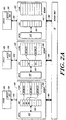
- Figure 2A depicts a preferred memory configuration providing data coherence in a multiprocessing system of the type, for example, described above.
- the illustrated system includes plural central processing units 40(A), 40(B) and 40(C) coupled, respectively, to associated memory elements 42(A), 42(B) and 42(C). Communications between the the processing and memory units of each pair are carried along buses 44A, 44B and 44C, as shown.
- the illustrated system further includes memory management element 46 for accessing information-representative signals stored in memory elements 44A, 44B and 44C via buses 48(A), 48(B) and 48(C), respectively.
- the central processing units 40A, 40B and 40C each include access request element, labelled 50A, 50B and 50C, respectively.
- These access request elements generate signals representative of requests for for access to an information stored in the memory elements 42A, 42B and 42C.
- the ownership-request signal representing requests for for priority access to an information-representative signal stored in the memories.
- access request elements 50A, 50B and 50C comprise a subset of an instruction subset implemented on CPU's 40A, 40B and 40C. This instruction subset is described below.
- the memory elements 40A, 40B and 40C include control elements 52A, 52B and 52C, respectively. Each of these control units interfaces a data storage area 54A, 54B and 54C via a corresponding directory element 56A, 56B and 56C, as shown.
- Stores 54A, 54B and 54C are utilized by the illustrated system to provide physical storage space for data and instruction signals needed by their respective central processing units. Thus, store 54A maintains data and control information used by CPU 40A, while stores 54B and 54C maintain such information used by central processing units 40B and 40C, respectively.
- the information signals maintained in each of the stores are identified by unique descriptors, corresponding to the signals' system addresses. Those descriptors are stored in address storage locations of the corresponding directory. While the descriptors are considered unique, multiple copies of some descriptors may exist among the memory elements 42A, 4B and 42C where those copies themselves identify copies of the same data element.
- Access request signals generated by the central processing units 40A, 40B and 40C include, along with other control information, an SA request portion matching the SA address of the requested information signal.
- the control elements 52A, 52B and 52C respond to access-request signals generated their respective central processing units 40A, 40B and 40C for determining whether the requested information-representative signal is stored in the corresponding storage element 54A, 54B and 54C. If so, that item of information is transferred for use by the requesting processor. If not, the control unit 52A, 52B, 52C transmits the access-request signal to said memory management element along lines 48A, 48B and 48C.
- the memory management element broadcasts an access-request signal received from the requesting central processing unit to the memory elements associated with the other central processing units.
- the memory management element effects comparison of the SA of an access request signal with the descriptors stored in the directories 56A, 56B and 56C of each of the memory elements to determine whether the requested signal is stored in any of those elements. If so, the requested signal, or a copy thereof, is transferred via the memory management element 46 to the memory element associated with the requesting central processing unit. If the requested information signal is not found among the memory elements 42A, 42B and 42C, the operating system can effect a search among the system's peripheral devices (not shown) in a manner described below.
- data coherency is maintained through action of the memory management element on memory stores 54A, 54B and 54C and their associated directories 56A, 56B and 56C. More particularly, following generation of an ownership-access request by a first CPU/memory pair (e.g., CPU 40C and its associated memory element 42C), the memory management element 46 effects allocation of space to hold the requested data in the store of the memory element of that pair (e.g., data store 54C of memory element 42C). Concurrent with the transfer of the requested information-representative signal from the memory element in which it was previously stored (e.g., memory element 42A), the memory management element deallocates that physical storage space which had been previously allocated for storage of the requested signal.
- a first CPU/memory pair e.g., CPU 40C and its associated memory element 42C
- the memory management element 46 effects allocation of space to hold the requested data in the store of the memory element of that pair (e.g., data store 54C of memory element 42C).
- the memory management element deallocates that physical
- the illustrated system stores information signals DATUM(3) and DATUM(2). Corresponding to each of those data elements are descriptors "car” and “bas,” retained in directory 56B. DATUM(2), and it. descriptor "bas,” are copied from store 42A and, therefore, retain the same labels.
- the system illustrated in Figure 2A does not store any data in the memory element 54C partnered to CPU 40C.
- Figure 2B illustrates actions effected by the memory management system 46A following issuance of an ownership-access request by one of the central processing units.
- the illustration depicts the movement of information signal DATUM(0) following issuance of an ownership-access request for that signal by CPU 40C.
- the memory management element 46 allocates physical storage space in the store 54C of the memory element partnered with CPU 40C.
- the memory management element 46 also moves the requested information signal DATUM(0) from store 54A, where it had previously been stored, to the requestor's store 54C, while concurrently deallocating that space in store 54A which had previously held the requested signal.
- the memory management element 46 Along with moving the requested information signal, the memory management element 46 also effects invalidation of the descriptor "foo" in directory 56A, where it had previously been used to identify DATUM(0) in store 54A, and reallocation of that same descriptor in directory 56C, where it will subsequently be used to identify the signal in store 54C.
- the memory management element 46 includes a mechanism for assigning access state information to the data and control signals stored in the memory elements 42A, 42B and 42C.
- These access states which include the invalid, read-only, owner and atomic states, govern the manner in which data may be accessed by specific processors.
- a datum which is stored in a memory element whose associated CPU maintains priority access over that datum is assigned an ownership state. While, a datum which is stored in a memory element whose associated CPU does not maintain priority access over that datum is assigned a read-only state. Further, a purported datum which associated with "bad" data is assigned the invalid state.
- Figure 3 depicts a preferred configuration for exemplary domain(0) segment 12A of Figure 1.
- the segment 12A includes processing cells 18A, 18B and 18C interconnected by cell interconnects 22A, 22B and 22c along bus segment 20A.
- Domain routing unit 28A provides an interconnection between the domain(0) segment 12A and if parent, domain(1) segment 14a of Figure 1. This routing unit 28A is coupled along bus 20A by way of cell interconnect 32A, as shown.
- the structure of illustrated bus segment 20A, as well as its interrelationship with cell interconnects 22A, 22B, 22C and 32A is more fully discussed in copending, European application no. EP-A-0322116.
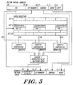
- FIG. 4 depicts a preferred structure for processing cells 18A, 18B . . . 18R.
- the illustrated processing cell 18A includes a central processing unit 58 coupled with external device interface 60, data subcache 62 and instruction subcache 64 over processor bus 66 and instruction bus 68, respectively.
- Interface 60 which provides communications with external devices, e.g., disk drives, over external device bus, is constructed in a manner conventional to the art.
- Processor 58 can comprise any one of several commercially available processors, for example, the Motorola 68000 CPU, adapted to interface subcaches 62 and 64, under control of a subcache co-execution unit acting through data and address control lines 69A and 69B, in a manner conventional to the art, and further adapted to execute memory instructions as described below.
- processors for example, the Motorola 68000 CPU, adapted to interface subcaches 62 and 64, under control of a subcache co-execution unit acting through data and address control lines 69A and 69B, in a manner conventional to the art, and further adapted to execute memory instructions as described below.
- Processing cell 18A further includes data memory units 72A and 72B coupled, via cache control units 74A and 74B, to cache bus 76.
- Cache control units 74C and 74D provide coupling between cache bus 76 and processing and data buses 66 and 68.
- bus 78 provides an interconnection between cache bus 76 and the domain(0) bus segment 20A associated with illustrated cell.
- data caches 72A and 72B dynamic random access memory devices, each capable of storing up to 8 Mbytes of data.
- the subcaches 62 and 64 are static random access memory devices, the former capable of storing up to 512k bytes of data, the latter of up to 256k bytes of instruction information.
- cache and processor buses 76 and 64 provide 64-bit transmission pathways, while instruction bus 68 provides a 32-bit transmission pathway.
- illustrated CPU 58 represents a conventional central processing unit and, more generally, any device capable of issuing memory requests, e.g., an i/o controller or other special purpose processing element.
- a multiprocessing system 10 constructed in accord with a preferred embodiment of the invention permits access to individual data elements stored within processing cells 18A, 18B, . . . 18R by reference to a unique system virtual address (SVA) associated with each datum.
- SVA system virtual address
- Implementation of this capability is provided by the combined actions of the memory management system 46, the subcaches 62, 64 and the caches 72A, 72B.
- the memory management system 46 includes cache control units 74A, 74B, 74C and 74D, with their related interface circuitry. It will further be appreciated that the aforementioned elements are collectively referred to as the "memory system.”
- storage accesses are considered “strongly ordered” if accesses to data by any one processor are initiated, issued and performed in program order and; if at the time when a store by processor I is observed by processor K, all accesses to data performed with respect to I before the issuing of the store must be performed with respect to K.
- storage accesses are weakly ordered if accesses to synchronizing variables are strongly ordered and; if no access to synchronizing variable is issued in a processor before all previous data accesses have been performed and; if no access to data is issued by a processor before a previous access to a synchronizing variable has been performed.
- the memory system stores data in units of pages and subpages, with each page containing 4k bytes and each subpage containing 64 bytes.
- the memory system allocates storage in the caches 74A, 74B on a page basis.
- Each page of SVA space is either entirely represented in the system or not represented at all.
- the memory system shares data between caches in units of subpages.
- the term "caches" refers to the cache storage elements 74A, 74B of the respective processing cells.
- SVA space within the illustrated system is a major departure from ordinary virtual memory schemes.
- Conventional architectures include a software controlled page-level translation mechanism that maps system addresses to physical memory addressor generates missing page exceptions.
- the software is responsible for multiplexing the page table(s) among all the segments in use.
- the memory system can handle a significant portion of the address space management normally performed by software in conventional architectures. These management responsibilities include:
- the illustrated system's processors e.g., processors 40A, 40B, 40C, communicate with the memory system via two primary logical interfaces.
- the first is the data access interface, which is implemented by the load and store instructions.
- the processor presents the memory system with an SVA and access mode information, and the memory system attempts to satisfy that access by finding the subpage containing the data and returning it.
- the second logical interface mode is control access, which is implemented by memory system control instructions.
- control access the processor instructs the memory system to perform some side effect or return some information other than the actual data from a page.
- system software uses control locations in SPA space for configuration, maintenance, fault recovery, and diagnosis.
- the caches e.g., elements 72A, 72B of cell 18A, stores information in units of pages, i.e.,4096 bytes. Each page of SVA space is either entirely present in the caches or not present at all.
- Each individual cache e.g., the combination of elements 72A and 72B of cell 18A, allocates space for data on a page by page basis.
- Each cache stores data on a subpage by subpage basis. Therefore, when a page of SVA space is resident in the system, the following are true:
- Each cache directory is made up of descriptors. There is one descriptor for each page of memory in a cache. At a particular time, each descriptor is either valid or invalid. If a descriptor is valid, then the corresponding cache memory page is associated with a page of SVA space, and the descriptor records the associated SVA page address and state information. If a descriptor is invalid, then the corresponding cache memory page is not in use.
- Each cache directory 46A acts as a content-addressable memory. This permits a cache to locate a descriptor for a particular page of SVA space without an iterative search through all of its descriptors.
- Each cache directory is implemented as a 32 way set-associative memory with 128 sets. All of the pages of SVA space are divided into 128 equivalence classes. A descriptor for a page can only be stored in the set of a cache directory that corresponds to the page's equivalence class. The equivalence class is selected by SVA[18:12]. At any given time, a cache can store no more than 32 pages with the same value for SVA[18:12], since that are 32 elements in each set.
- SVA[18:12] selects a set. Each of the descriptors in the selected set is simultaneously compared against SVA[63:19]. If one of the elements of the set is a descriptor for the desired page, the corresponding comparator will indicate a match.
- the index in the set of the matching descriptor concatenated with the set number, identifies a page in the cache. If no descriptor in the set matches, the cache signals a missing_page exception. If more than one descriptor matches, the cache signals a multiple_descriptor_match exception.
- SVA[18:12] is used as a hash function over SVA addresses to select a set.
- System software assigns SVA addresses so that this hash function gives good performance in common cases. Two important distribution cases are produced by referencing many pages of a single segment and by referencing the first page of many segments.
- SVA[18:12] to select a cache set produces good cache behavior for contiguous groups of pages, since 128 contiguous pages can all reside in a set. However, this key produces poor hashing behavior for many pages with the same value in that field.
- System software avoids this situation by applying a hash function when allocating SVA space to context segments.
- descriptors contain the following fields, the bit-size of each of which is indicated in parentheses:
- descriptor.no_write If descriptor.no_write is set, write accesses to the page result in a page_no_write exception.
- System software can trap page reads by keeping a table of pages to be trapped, and refusing to create an SVA page for them. Then, it can translate missing_page exceptions into software generated page_no_read exceptions.
- Descriptor.no_write can be used to implement an copy-on-access scheme, which in turn can be used as an approximation of 'copy-on-write.'
- the pages of the forking process's address space are set to take page_no_write exceptions.
- the child process's address space segments are left sparse.
- the page fault is satisfied by making a copy of the corresponding page of the parent process, and the descriptor.no_write is cleared for that page. If the parent writes a page before the child has copied it, the page_no_write handler copies the page into the child address space and then clears descriptor.no_write.
- descriptor.held is 1 in a descriptor, then the descriptor's cache is prevented from invalidating it.
- all of the field of the descriptor except descriptor.tag, descriptor.held, descriptor.LRU_insert_index and descriptor.LRU_insert_priority are reinitialized as if the descriptor had not existed when the subpage arrived.
- Descriptor.held is not propagated from one cache to another.
- Descriptor.owner_limit limits ownership of subpages of the page to a particular cache or domain(0) in the system bus hierarchy.
- the following list shows the values of descriptor.owner_limit, and the semantics from the point of view of an owning cache responding to requests from other caches.
- Descriptor.owner_limit is propagated to other caches as follows: so long as all of the subpages of a descriptor are read-only copies, descriptor.owner_limit is always Default_owner_limit. When a new cache becomes the owner of a subpage, it copies the value of descriptor.owner_limit from the old owner.
- descriptor.no_owner is 1 in a descriptor, then the descriptor's cache cannot acquire an ownership state for any subpages of the page described by the descriptor.
- a cache containing a descriptor with descriptor.no_owner of 1 never responds to requests from other caches except to indicate that it is holding the copy.
- Descriptor.no_owner is not propagated from one cache to another.
- descriptor.no_atomic is 1 in a descriptor, then the descriptors cache cannot acquire atomic or pending atomic ownership states for any subpages of the page described by the descriptor.
- a processor attempt to set atomic or pending atomic ownership state fails, and is signalled back to the processor.
- the processor signals a page_no_atomic exception.
- Descriptor.no_atomic is propagated from one cache to another.
- Descriptor summarizes subpage state field corresponding to four consecutive subpages. There is one two-bit field for each of the 12 sets of four subpages represented by the descriptor. The following is a list of summary states:
- the illustrated memory elements detect errors, for example, while executing a synchronous request from its local processor.
- the element signals the error in its response to the request.
- the local processor then signals a corresponding exception.
- a memory element detects an error while executing a request from a remote cell, it sends an interrupt to its local processor and responds to the request with an error reply.
- the expression "the cache signals an exception” is an abbreviation for this process.
- Each memory includes a Cache Activity Descriptor Table (CADT) (not shown), in which it maintains the status of ongoing activities.
- Cache Activity Descriptor Table (CADT) (not shown), in which it maintains the status of ongoing activities.
- a memory element detects an error in responding to a request from its domain(0) or in executing an asynchronous control instruction or a remote control instruction, it notes the error in a descriptor in the CADT before sending an interrupt.
- Software reads the CADT to identify the particular source and type of error.
- Software resets the CADT to acknowledge receipt of the error.
- each of its subpages is resident in one or more of the caches.
- the descriptor in that cache for the page containing that subpage records the presence of that subpage in one of several states.
- the state of the subpage in a cache determines two things:
- the states of subpages in caches change over time as user programs request operations that require particular states.
- a set of transition rules specify the changes in subpage states that result from processor requests and inter-cache domain communications.
- the processors local cache communicates over the domains to acquire a copy of the subpage and/or to acquire the necessary state for the subpage. If the cache fails to satisfy the request, it returns an error indication to the processor, which signals an appropriate exception.
- the instruction set includes several different forms of loan and store instructions that permit programs to request subpage states appropriate to the expected future data reference pattern of the current thread of control, as well as protocol between different threads of control in a parallel application.
- the states and their transitions are described in three groups.
- the first group are the basic states and transitions that implement the strongly ordered, sequentially consistent model of memory access.
- Second are the additional states that implement the transaction primitives.
- the transient states which improve the performance of the memory system, are presented.
- the processor subcaching system is divided into two sides: data and instruction.
- the data subcache 62 is organized in 64 bit words, like the cache.
- the instruction subcache 64 is organized into 32 bit half-words, since there re two 32 bit instructions in each 64 bit memory word.
- the data subcache stores .5Mbyte, and the instruction subcache .25Mbyte. Since the items in the instruction subcache are half-words, the two subcaches store the same number of items.
- the two sides of the subcache are similar in structure to the cache.
- Subcache descriptors do not describe entire pages of SVA space. They describe different units, called blocks. The size of a block is different on the two sides of the subcache. On the data side, blocks are the half the size of pages. On the instruction side, they are one quarter as large as pages. On both sides, each block is divided into 32 subblocks. The following table shows the relative sizes of blocks, subblocks and other items in the two subcaches.
- the subcache allocates pages and copies data one subblock at a time.
- the subcaches 62, 64 are organized similarly to the caches. Where the caches are 32-way set associative (each set contains 32 descriptors), the subcaches are 4 way set-associative. For the data side, the set number is bits [16:11] of the SVA, and the tag bits [63:17]. For the instruction side, the set number is bits [15:10], and the tag is bits [63:16].
- the data subcaches maintain modification information for each subblock.
- each subcache implements a simple approximation of the cache LRU scheme.
- each subcache maintains the identity of the most recently referenced descriptor.
- a descriptor is needed, one of the three descriptors that is not the most recently referenced descriptor is selected at random for replacement.
- the data subcaches write modified subblocks to their caches as described above in the section entitled 'Updates from the Subcache to the Cache.'
- the basic model of data sharing is defined in terms of three classes of subpage states: invalid, read-only, and owner. These three classes are ordered in strength according to the access that they permit; invalid states permit no access, read-only states permit load access, and owner states permit load and store access. Only one cache may hold a particular subpage in an owner state at any given time. The cache that holds a subpage in an owner state is called the owner of the subpage. Ownership of each subpage moves from cache to cache as processors request ownership via store instructions and special load instructions that request ownership. Any number of caches may hold a particular subpage in a read-only state.
- a subpage When a subpage is not present in a cache, it is said to be in an invalid state with respect to that cache. If a processor requests a load or store to a subpage which is in an invalid state in its local cache, then that cache must request a copy of the subpage in some other state in order to satisfy the data access. There are two invalid states: invalid descriptor and invalid. When a particular cache has no descriptor for a particular page, then all of the subpages of that page are said to be in invalid descriptor state in that cache. Thus, subpages in invalid descriptor state are not explicitly represented. When a particular cache has a descriptor for a particular page, but a particular subpage is not present in that cache, then that subpage is in invalid state.
- the two invalid states are distinguished because it is much easier for a subpage to undergo a transition to a read-only or owner state from invalid than from invalid descriptor.
- a descriptor is already present.
- a descriptor must be allocated.
- Non-exclusive and exclusive There are two basic owner states: non-exclusive and exclusive. When a particular cache holds a particular subpage in non-exclusive state, any number of other caches may simultaneously hold that subpage in read-only state. When a particular cache holds a particular subpage in exclusive state, then no other cache may hold a copy so long as that cache retains exclusive state. When a cache holds a subpage in non-exclusive state, and the data in that subpage are modified, then that cache sends the modified data to all of the caches with read-only copies.
- the basic state transitions can be illustrated by considering a subpage in exclusive state on a particular cache.
- the basic mechanism by which data moves from this first cache to other caches is the execution of load and store instructions by processors other than the local processor of that first cache.
- the different load and store instructions, as well as the prefetch instructions permit programs to request that their local cache acquired read-only, non-exclusive, or exclusive state. If another cache requests read-only state, then the first cache reduces its state from exclusive to non-exclusive and grants read-only state to the requestor. If another cache requests non-exclusive state, then the first cache reduces its state to read-only and grants non-exclusive state to the requestor. If another cache requests exclusive state, then the first cache reduces its state to invalid and grants exclusive state to the requestor.
- Ownership moves from cache to cache as processors request exclusive and non-exclusive states. When a cache requests non-exclusive ownership, any read-only copies are invalidated (undergo a transition to an invalid state).
- a cache When a cache acquires ownership of a subpage in order to satisfy a store instruction, it does not grant that ownership to another cache until the store instruction is complete. In the case of non-exclusive state, a cache does not grant ownership to another cache until the new data from the store is sent to the caches with read-only copies.
- This rule provides the strongly ordered nature of the memory system, in that it ensures readers of a memory location to see modifications in the order that they are made.
- the memory system includes two mechanisms for avoiding unnecessary non-exclusive owner states.
- a non-exclusive owner sends an update out over the domains, it receives a return receipt that includes whether any other caches actually hold read-only copies. It the receipt indicates that there are no read-only copies, then the owner changes the subpage's state from non-exclusive to exclusive, avoiding future updates.
- a cache receives an update for a subpage that it holds in read-only state, its action depends on whether that subpage is currently resident in the CPU's subcache.
- the cache invalidates it. If the subpage is cached, then the cache removes it from the subcache. The effect of these actions is as follows: So long as a subpage is not modified, read-only copies of it propagate throughout the memory system. When a subpage is modified, each read-only copy persists only if that copy is referenced at least as frequently as the subpage is modified.
- the synchronization states and related transitions implement the KSR transaction model.
- the transaction model is a primitive synchronization mechanism that can be used to implement a wide variety of synchronization protocols between programs. All of these protocols share the purpose of imposing an orderly structure in time on accesses to shared data.
- the transaction model is based on two states, atomic and pending atomic, a set of instructions that explicitly request transitions to and from these states, and forms of the load and store instructions whose semantics are dependent on whether the subpage that they reference is currently in atomic state.
- the atomic state is the central feature of the transaction model. Atomic state is a stronger form of ownership than exclusive state. Subpage only enter and leave atomic state as a result of explicit requests by programs.
- atomic state can be used to single-thread access to any subpage in SVA space.
- a processor executes an instruction that requests that a subpage enter atomic state, the instruction will only complete normally if the subpage is not in atomic state already.
- atomic state on a subpage can be used as a simple lock. The lock is locked by taking the subpage atomic, and unlocked by releasing it to exclusive.
- a program requests that a subpage enter atomic state with one of the forms of the get instruction, and releases it with the rsp instruction. These instructions are described in more detail below.
- a sequence of get, manipulate some protected information, and rsp is the simplest form of transaction.
- the following sections present more complex features of the transaction mechanism that permit the implementation of more sophisticated protocols. These protocols provide high performance for particular parallel programming applications.
- a subpage In simple transactions, a subpage is used purely as a lock. The data in the subpage is not relevant. Some of the more sophisticated forms of synchronization mechanisms make use of the data in a subpage held in atomic state. The simplest case is to use atomic state on a subpage as a lock on the data in that subpage. Programs take one or more subpages into atomic state, manipulate their contents, and release them.
- Non-blocking load instructions access the data in a subpage regardless of whether or not that subpage is in atomic state. These are used by ordinary programs and by the single-threaded transactions described above. Blocking load instructions only proceed normally if the subpage is not in atomic state. If the subpage referenced by a blocking load instruction is in atomic state, the instruction blocks until the subpage leaves atomic state. In a producer-consumer relationship, the producer(s) hold the subpage(s) containing the data in atomic state, while the consumers read the data using blocking load instructions.
- the get instructions actively request atomic state over the domains may have absolute knowledge that a particular subpage is already in atomic state. In this case, sending a request across the domains is pointless. Instead, the program can use the stop instruction to place the subpage in pending atomic state in the local cache, and depend upon another program to expel the subpage using the rspe instruction.
- a subpage When a subpage is in pending atomic state in a particular cache, this indicates that atomic state is desired in that cache. If a message arrives over the domains in a cache that holds a particular subpage in pending atomic state that indicates that atomic state is available for that subpage, then that cache will take the subpage in atomic state.
- a processor executes a stop instruction for a subpage, that subpage is placed in pending atomic state on the local cache.
- another processor executes an rspe instruction, a message is sent across the domains indicating that atomic state is available for the subpage. When this message reaches a cache with the subpage in pending atomic state, that cache acquires atomic state.
- the transitive states are used automatically by the memory system to improve the performance of accesses to subpages in case of contention.
- a particular subpage enters a transient state in a particular cache when that cache receives a request for the subpage to which it cannot respond immediately. If a subpage is in atomic state and another cache requests that subpage, that subpage enters transient atomic state in the holding cache.
- the transient state forces the subpage to be expelled as if an rspe had been used.
- a subpage enters a transient state on a cache due to a request by a single other cache.
- any number of additional caches may make requests for the same subpage before the holding cache expels it.
- the single expulsion satisfies all of the requesting caches with a single message over the domains.
- Multiple read/writer sharing is multiple read-only copies with high temporal locality and write updates with lower temporal locality. Retaining read-only copies is most efficient since multiple copies are read multiple times between updates. Updates take place in a single domain operation.
- Single read/writer access is multiple read-only copies read-only copies with low temporal locality and write updates with much higher locality. Retaining read-only copies is less efficient since copies are updated multiple times between updates.
- a single read/write copy (exclusive owner state) does not require a domain operation for write update. Applying these two cases independently to all read-only copies allows transition from non-exclusive ownership with multiple read-only copies to exclusive ownership with no read-only copies. The strategy for balancing these considerations is as follows:
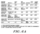
- the tables shown in Figures 6A and 6B provide the precise specification of the action that a cache takes in response to data access requests from its local processor. There is one row of the table for each processor request to the cache. There is a column for each possible state of the subpage in the cache.
- the entry in the table states the message, if any, sent over the domains by a cache to satisfy the request when the subpage is in the specified state in that cache.
- the messages are defined below.
- the local cache sets the subpage in state state after receiving a successful response to the message.
- Caches send messages over the domains to acquire copies of subpages in particular states.
- Each message consists of a request type, a descriptor, and the data for a subpage.
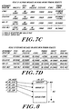
- the tables shown in Figures 7, 7A, 7B, 7C, and 7D provide the precise specification of how each cache responds to messages on the domain.
- the tables are divided into three sections: read operations, write operations, and response operations. Each section includes the definition of the operations.
- the tables give the state that results when a cache with a subpage in a specified state receives a particular message. In addition to the states, the tables are annotated with the following side effects and modifications:
- read operations are used to acquire the state necessary for a processor operation. Once the subpage has been 'read' into the local cache, the operation can proceed.
- read messages are simply requests for the subpage in a particular state, and are named after the state. For example, read atomic requests atomic state.
- write operations are used to send modified data out to other caches or to force other caches to give up state.
- descriptor.owner_limit When descriptor.owner limit is Domain0_owner_limit, a recombine message is not delivered outside of the originating domain(0). When descriptor.owner_limit is Cache_owner_limit, a recombine message is never sent. Note that the indication "recombine?" indicates the LRU position comparison described above.
- response messages are sent by caches that respond to read messages.
- the first table shows the action, if any, taken for a response message by a cache that already holds the subpage in the specified state.
- the second table shows the action of a cache that is awaiting a response to the specified type of request for the subpage. There are two cases shown in the tables:
- a cache When a cache receives a copy of a subpage in invalid descriptor state, it initializes its descriptor by copying most of the fields of the descriptor on the source cache. LRS_position, LRU insert , index, subcache, subpage_state, held and no_ owner are never copied. Owner_limit is handled specifically.
- a processor makes data requests to its local cache to satisfy load and store instructions and co-processor operations.
- a cache makes requests to its local processor to force the processor to invalidate its copy of a subpage in subcache.
- a processor passes load and store instructions to its local cache as requests when the subpage containing the referenced address is not present in the subcache in the required state.
- the different types of load and store instructions pass information to the local cache about the access patterns of the following instructions. For example, if the sequence of the instructions is a load followed by a store, and the subpage containing the data item is not yet resident in the local cache, it is more efficient to acquire ownership for the load than to get a read-only copy for the load instruction and then communicate over the domains a second time to acquire ownership for the store instruction.
- load and store instructions are described below. Each description begins with a brief summary of the semantics of the instruction, and continues with a detailed description of the cache's action.
- All of the load instructions described here have two forms: blocking and non-blocking. These forms control the behavior of the load instructions with respect to atomic state. If a processor executes a blocking load instruction that references a subpage in atomic state, that instruction will wait until the subpage leaves atomic state before proceeding. If a processor executes a non-blocking load instruction that references a subpage in atomic state, that instruction will acquire atomic state in the local cache and proceed.
- the subpage atomic instructions are the program interface to the get, stop, and release operations described above. These instructions exist in several forms to permit precise tuning of parallel programs.
- a processor propagates modified information to its local cache with an Update data request.
- a cache forces its local processor to remove a subpage from subcache in order to invalidate the subpage in response to a request from another cache.
- each cache responds to messages from other caches delivered by its local domain(0).
- a read message requests some other cache to respond with the data for a subpage.
- Each read message also requests a particular state, and both the cache that responds with the data and other caches with copies change the state of their copy of the subpage in order to satisfy the state request.
- a write message either supplies an updated copy of a subpage to caches with read-only copies, or directs other caches to change the state of their copies.
- a response message is sent in response to a read message. Caches other than the original requestor take actions on response messages as specified below.
- read and write message do not correspond to load and store instructions. Both load and store instructions result in read messages to acquire a copy of the subpage in the appropriate state. A particular store instruction will not result in an immediate write message unless the subpage is held in nonexclusive state.
- the caches of a KSR system can be used by system software as part of a multilevel storage system.
- physical memory is multiplexed over a large address space via demand paging.
- the caches include features that accelerate the implementation of a multi-level storage system in which software moves data between the caches and secondary storage in units of SVA pages.
- each cache approximately orders the pages from Most Recently Used (MRU) to Least Recently Used (LRU).
- MRU Most Recently Used
- LRU Least Recently Used
- each cache maintains an approximate measurement of the working set of the cache.
- the working set is a measurement of the number of pages which are in steady use by programs running on a cache's local processor over time, as distinct from pages referenced a few times or infrequently.
- Software measures the working set of each cache as a point between MRU and LRU. Pages above the working set point are in the working set, while pages below have left the working set.
- the working set information accelerates a software strategy that treats the non-working set portion of each cache's memory as system backing store.
- each cache includes facilities to automatically move and remove pages in parallel with other computation to avoid the need for frequent software intervention required by full sets. These facilities use the LRU and working set information to:
- Each cache recombines pages from LRU up to the working set point, it is significantly less likely to be referenced again that if it is above the working set point. Therefore, each cache recombine. pages when they pass the working set point.
- a cache uses the write exclusive recombine or write non-exclusive recombine message for each subpage to recombine a page. If the recombine messages fail to find another cache to take over the page, the recombining cache retains the data. If the recombine messages fail to find another cache to take over the page, the recombining cache retains the data. In effect, it has found itself as the target of the recombine. Since pages are recombined as soon as possible after they leave the working set, any other cache with copies is likely to have the page in the working set. (were it not in the working set in some other cache, that cache would have recombined it.)
- a cache will automatically drop a page which is below the working set point and which has subpages in read-only or invalid state (a read-only page). If a cache has no free descriptors and cannot allocate a descriptor by recombining a page, it will drop a read-only page that is not subcached and is anywhere in the MRU-LRU order. If a cache has no read-only pages, it will drop an unmodified page with subpages in invalid, read-only, or exclusive state that is not subcached and is in the lower portion of the working set, as defined by the WS_Low register defined below.
- Software sometimes has knowledge of the expected reference pattern for some data. If software expects a page to be referenced only one, that page should be put into the LRU order someplace below MRU, to avoid displacing information that is more likely to be used later. In particular, if software is prefetching data that it won't reference for a while, and perhaps not reference it at all, it should not be inserted at MRU. Software controls the insertion point by setting the appropriate LRU_insert_index in the prefetch and chng instructions.
- Each cache maintains LRU state for all of the resident pages.
- the LRU data is maintained separately for each of the 128 sets of the descriptor associative memory, and orders the 32 pages in the set according to their approximate time of last reference.
- Each cache maintains an LRU ⁇ MRU ordering of the descriptors in each set. The ordering is maintained in descriptor.LRU_priority.
- Each of the descriptors in a set has a value from (MRU) to 31 (LRU) in descriptor.LRU_priority.
- descriptor.LRU_priority When a page is first subcached, descriptor.LRU_priority is set to zero, which inserts it at MRU. When the last subcached subpage of a page is evicted from the subcache, descriptor.LRU_priority is set as specified by descriptor.LRU_insert_index. The insert index selects an entry in LRU_insert_table, a per-cache table described below. descriptor.LRU_priority is set to
- LRU_insert_table (descriptor.LRU_insert_index) and the descriptor.LRU_priority is changed for other descriptors as appropriate to accommodate it. Note that if an entry of the LRU_insert_table is set close enough to MRU, then pages evicted from subcache will be inserted closer to MRU than pages in subcache.
- Each cache has an array of 32 working set rate counters, 16 bits. The counters freeze at 2 16 -1.
- the bucket corresponding to its current LRU position is incremented.
- software can determine the approximate working set size. Software can attempt to maintain the working set for each schedulable entity, or it can just run a set of entities on a cache and maintain the aggregate working set. The later incurs less cost at scheduling time.
- Subcached pages complicate working set measurement.
- the LRU value of a page can change any time that some other page moves into the cache.
- the LRU numbers do not consider whether or not a page is subcached. Instead, all the hardware mechanisms which use LRU consider all subcached pages as one LRU level, and all non-subcached pages at various other LRU levels.
- the LRU_insert_table maps from four logical points in the LRU ⁇ MRU sequence to the 32 actual slots in the set.
- the four slots are named:
- the cache proceeds through as many of the following actions needed to find a usable descriptor:
- the cache uses otherwise idle time to recombine pages. If Recombine_high_limit is not 31, then the background task scans across the sets looking for pages in each set that can be recombined and recombines them.
- Allocation recombines and automatic recombines will generally recombine pages as they leave the working set. There will be few recombinable pages in backing store. If at some time there are not recombinable pages in a cache, new recombinable pages will appear in the form of pages dropping out of the working set. If background and allocation recombines keep up with this rate, the only source of recombinable pages in the backing store will be references by other caches to pages in backing store. The referencing caches' descriptors will probably be in their working sets, and so recombining the pages to them is appropriate.
- LRU_insert_index When one of these instructions moves the first subpage for a page into subcache, the LRU_insert_index in the instruction replaces descriptor.LRU_insert_index for that page. Then, when the page leaves subcache, it is inserted into the LRU according to the specified entry in the LRU_insert_table.
- the chng instruction and the various prefetch instructions permit the programmer to specify an LRU_insert_index. When a cache executes one of these instructions for a subpage of a page which has no valid subpages, the specified LRU_insert_index becomes descriptor.LRU_insert_index.
- the LRU insert index specified in control instruction replaces the index previously stored in the descriptor. Once the index is set in a cache, it persists in that cache until it is reset or all of the subpages become invalid. In effect, the memory system has a limited memory for LRU bias information. If one program indicates that a page is likely to be referenced again, and shortly thereafter another program indicates that it is unlikely to be referenced again, the second indication persists.
- System software can establish a different default behavior. For example, system software might include a background task that changes descriptor.LRU_insert_index to WS_High for pages below BS_High. This would implement a policy as follows: once a page had aged to backing store, any LRU insert index information was too old to be valuable, and the ordinary default should apply instead.
- Prefetching requires care in the use of LRU insertion bias. It is desirable for software to be able to 'over prefetch,' to prefetch any data that it may need. To avoid driving higher priority information out of the LRU, the over-prefetched pages should be fetched with an LRU_insert_index other than WS_High.
- Figure 9 depicts an exemplary domain routing unit 28F constructed according to a preferred practice of the invention.
- the unit 28F includes domain directory section 80 and remote fiber interface section 82 interconnected via cache bus 76.
- Directory section 80 includes dual routing control units 84A and 84B coupled to memory stores 86A and 86B, as illustrated.
- the stores comprise 8 Mbyte dynamic random access memory elements arranged for storing lists of the descriptors identifying data maintained in the domain segments which descend from the upper level domain segment to which the illustrated routing unit 28F is attached.
- Routing control units 84A and 84B are constructed and operate similarly to the cache control units 74A, 74B, 74C and 74D, described above.
- the units additionally include hash encoding logic for controlling storage and access of descriptors within stores 86A and 86B. This encoding logic, as well as the descriptor storage and access mechanisms, are conventional in the art.
- the remote fiber interface section 82 includes remote interface unit 88, coupled with fiber receiver and decoding section 90 and with fiber encoding and transmitting section 92, in the manner illustrated in Figure 9.
- the receiver 90 interfaces the incoming fiber optic line 94, while the transmitter 92 interfaces the outgoing line 96.
- the unit 88 provides CRC encoding and decoding for the fiber optic link.
- Receiver 90 and transmitter 92 are constructed in accord with techniques conventional in the art.
- domain routing unit 28F is specifically configured to interface remote domain segments (see, for example, segments 12F and 14B of Figure 1)
- direct interconnect units i.e., those domain routing units which provide interconnection between non-remote segments, e.g., segments 14A and 12A of Figure 1
- the remote fiber interface section 82 is replaced by a local interface section, which provides buffering for transmissions between respective domain segment buses.
- a multiprocessing system constructed in accord with the invention features improved data coherency, reduced latency and bus contention, as well as unlimited scalability.
Landscapes
- Engineering & Computer Science (AREA)
- Theoretical Computer Science (AREA)
- Software Systems (AREA)
- Physics & Mathematics (AREA)
- General Physics & Mathematics (AREA)
- General Engineering & Computer Science (AREA)
- Quality & Reliability (AREA)
- Signal Processing (AREA)
- Computer Networks & Wireless Communication (AREA)
- Mathematical Physics (AREA)
- Multimedia (AREA)
- Memory System Of A Hierarchy Structure (AREA)
- Multi Processors (AREA)
- Information Retrieval, Db Structures And Fs Structures Therefor (AREA)
Applications Claiming Priority (3)
| Application Number | Priority Date | Filing Date | Title |
|---|---|---|---|
| US136930 | 1987-12-22 | ||
| US07/136,930 US5055999A (en) | 1987-12-22 | 1987-12-22 | Multiprocessor digital data processing system |
| EP88311139A EP0322117B1 (de) | 1987-12-22 | 1988-11-24 | Multiprozessor-Digitaldatenverarbeitungssystem |
Related Parent Applications (1)
| Application Number | Title | Priority Date | Filing Date |
|---|---|---|---|
| EP88311139A Division EP0322117B1 (de) | 1987-12-22 | 1988-11-24 | Multiprozessor-Digitaldatenverarbeitungssystem |
Publications (1)
| Publication Number | Publication Date |
|---|---|
| EP1016971A2 true EP1016971A2 (de) | 2000-07-05 |
Family
ID=22475061
Family Applications (6)
| Application Number | Title | Priority Date | Filing Date |
|---|---|---|---|
| EP00200995A Withdrawn EP1020799A2 (de) | 1987-12-22 | 1988-11-24 | Multiprozessor-Digitaldatenverarbeitungssystem |
| EP00200994A Withdrawn EP1016971A2 (de) | 1987-12-22 | 1988-11-24 | Multiprozessor-Digitaldatenverarbeitungssystem |
| EP19910116719 Withdrawn EP0468542A3 (en) | 1987-12-22 | 1988-11-24 | Multiprocessor digital data processing system |
| EP93120309A Expired - Lifetime EP0593100B1 (de) | 1987-12-22 | 1988-11-24 | Multiprozessor-Digitaldatenverarbeitungssystem und Verfahren zum Betreiben dieses Systems |
| EP00200993A Withdrawn EP1016979A2 (de) | 1987-12-22 | 1988-11-24 | Multiprozessor-Digitaldatenverarbeitungssystem |
| EP88311139A Expired - Lifetime EP0322117B1 (de) | 1987-12-22 | 1988-11-24 | Multiprozessor-Digitaldatenverarbeitungssystem |
Family Applications Before (1)
| Application Number | Title | Priority Date | Filing Date |
|---|---|---|---|
| EP00200995A Withdrawn EP1020799A2 (de) | 1987-12-22 | 1988-11-24 | Multiprozessor-Digitaldatenverarbeitungssystem |
Family Applications After (4)
| Application Number | Title | Priority Date | Filing Date |
|---|---|---|---|
| EP19910116719 Withdrawn EP0468542A3 (en) | 1987-12-22 | 1988-11-24 | Multiprocessor digital data processing system |
| EP93120309A Expired - Lifetime EP0593100B1 (de) | 1987-12-22 | 1988-11-24 | Multiprozessor-Digitaldatenverarbeitungssystem und Verfahren zum Betreiben dieses Systems |
| EP00200993A Withdrawn EP1016979A2 (de) | 1987-12-22 | 1988-11-24 | Multiprozessor-Digitaldatenverarbeitungssystem |
| EP88311139A Expired - Lifetime EP0322117B1 (de) | 1987-12-22 | 1988-11-24 | Multiprozessor-Digitaldatenverarbeitungssystem |
Country Status (6)
| Country | Link |
|---|---|
| US (5) | US5055999A (de) |
| EP (6) | EP1020799A2 (de) |
| JP (1) | JP2780032B2 (de) |
| AT (2) | ATE198673T1 (de) |
| CA (1) | CA1333727C (de) |
| DE (2) | DE3856552T2 (de) |
Cited By (2)
| Publication number | Priority date | Publication date | Assignee | Title |
|---|---|---|---|---|
| CN110293539A (zh) * | 2019-06-24 | 2019-10-01 | 佛山智异科技开发有限公司 | 工业机器人示教器软件架构的实现方法、装置及示教器 |
| CN110399313A (zh) * | 2018-04-25 | 2019-11-01 | Emc知识产权控股有限公司 | 用于提高缓存性能的系统和方法 |
Families Citing this family (206)
| Publication number | Priority date | Publication date | Assignee | Title |
|---|---|---|---|---|
| US5282201A (en) * | 1987-12-22 | 1994-01-25 | Kendall Square Research Corporation | Dynamic packet routing network |
| US5335325A (en) * | 1987-12-22 | 1994-08-02 | Kendall Square Research Corporation | High-speed packet switching apparatus and method |
| US5055999A (en) * | 1987-12-22 | 1991-10-08 | Kendall Square Research Corporation | Multiprocessor digital data processing system |
| US5341483A (en) * | 1987-12-22 | 1994-08-23 | Kendall Square Research Corporation | Dynamic hierarchial associative memory |
| US5251308A (en) * | 1987-12-22 | 1993-10-05 | Kendall Square Research Corporation | Shared memory multiprocessor with data hiding and post-store |
| US5761413A (en) * | 1987-12-22 | 1998-06-02 | Sun Microsystems, Inc. | Fault containment system for multiprocessor with shared memory |
| US5822578A (en) * | 1987-12-22 | 1998-10-13 | Sun Microsystems, Inc. | System for inserting instructions into processor instruction stream in order to perform interrupt processing |
| US5226039A (en) * | 1987-12-22 | 1993-07-06 | Kendall Square Research Corporation | Packet routing switch |
| EP0330425B1 (de) * | 1988-02-23 | 1995-12-06 | Digital Equipment Corporation | Symmetrische Steuerungsanordnung für Multiverarbeitung |
| US5136717A (en) * | 1988-11-23 | 1992-08-04 | Flavors Technology Inc. | Realtime systolic, multiple-instruction, single-data parallel computer system |
| US5371874A (en) * | 1989-01-27 | 1994-12-06 | Digital Equipment Corporation | Write-read/write-pass memory subsystem cycle |
| JPH0833958B2 (ja) * | 1989-05-30 | 1996-03-29 | 沖電気工業株式会社 | 顧客情報処理システム |
| CA2019300C (en) | 1989-06-22 | 2001-06-12 | Kendall Square Research Corporation | Multiprocessor system with shared memory |
| JPH0362257A (ja) * | 1989-07-31 | 1991-03-18 | Toshiba Corp | ネットワークモニタリングシステム |
| US5230070A (en) * | 1989-09-08 | 1993-07-20 | International Business Machines Corporation | Access authorization table for multi-processor caches |
| US5265227A (en) * | 1989-11-14 | 1993-11-23 | Intel Corporation | Parallel protection checking in an address translation look-aside buffer |
| JP2665813B2 (ja) * | 1990-02-23 | 1997-10-22 | 三菱電機株式会社 | 記憶制御装置 |
| EP0447736B1 (de) * | 1990-03-19 | 1995-09-27 | BULL HN INFORMATION SYSTEMS ITALIA S.p.A. | Mehrrechnersystem mit verteilten gemeinsamen Betriebsmitteln und dynamischer und selektiver Vervielfältigung globaler Daten und Verfahren dafür |
| US5410691A (en) * | 1990-05-07 | 1995-04-25 | Next Computer, Inc. | Method and apparatus for providing a network configuration database |
| ATE231259T1 (de) * | 1990-05-18 | 2003-02-15 | Sun Microsystems Inc | Dynamischer hierarchischer leitwegverzeichnisorganisationsassoziativspeich r |
| DE69127773T2 (de) * | 1990-06-15 | 1998-04-02 | Compaq Computer Corp | Vorrichtung zur echten LRU-Ersetzung |
| JPH0476681A (ja) * | 1990-07-13 | 1992-03-11 | Mitsubishi Electric Corp | マイクロコンピュータ |
| US5261069A (en) * | 1990-08-13 | 1993-11-09 | Hewlett-Packard Company | Method of maintaining consistency of cached data in a database system |
| US5530941A (en) * | 1990-08-06 | 1996-06-25 | Ncr Corporation | System and method for prefetching data from a main computer memory into a cache memory |
| DE69130967T2 (de) * | 1990-08-06 | 1999-10-21 | Ncr International, Inc. | Rechnerspeicheranordnung |
| US5339397A (en) * | 1990-10-12 | 1994-08-16 | International Business Machines Corporation | Hardware primary directory lock |
| US5829030A (en) * | 1990-11-05 | 1998-10-27 | Mitsubishi Denki Kabushiki Kaisha | System for performing cache flush transactions from interconnected processor modules to paired memory modules |
| US5313647A (en) * | 1991-09-20 | 1994-05-17 | Kendall Square Research Corporation | Digital data processor with improved checkpointing and forking |
| CA2078312A1 (en) * | 1991-09-20 | 1993-03-21 | Mark A. Kaufman | Digital data processor with improved paging |
| CA2078315A1 (en) * | 1991-09-20 | 1993-03-21 | Christopher L. Reeve | Parallel processing apparatus and method for utilizing tiling |
| US5245563A (en) * | 1991-09-20 | 1993-09-14 | Kendall Square Research Corporation | Fast control for round unit |
| JP3182806B2 (ja) * | 1991-09-20 | 2001-07-03 | 株式会社日立製作所 | バージョンアップ方法 |
| CA2078310A1 (en) * | 1991-09-20 | 1993-03-21 | Mark A. Kaufman | Digital processor with distributed memory system |
| CA2078311A1 (en) * | 1991-09-23 | 1993-03-24 | Sun Microsystems, Inc. | Fault containment system for multiprocessor with shared memory |
| EP0543032A1 (de) * | 1991-11-16 | 1993-05-26 | International Business Machines Corporation | Erweitertes Speicheradressierungsschema |
| US5493663A (en) * | 1992-04-22 | 1996-02-20 | International Business Machines Corporation | Method and apparatus for predetermining pages for swapping from physical memory in accordance with the number of accesses |
| US5432917A (en) * | 1992-04-22 | 1995-07-11 | International Business Machines Corporation | Tabulation of multi-bit vector history |
| US5428803A (en) * | 1992-07-10 | 1995-06-27 | Cray Research, Inc. | Method and apparatus for a unified parallel processing architecture |
| US5361385A (en) * | 1992-08-26 | 1994-11-01 | Reuven Bakalash | Parallel computing system for volumetric modeling, data processing and visualization |
| US5418966A (en) * | 1992-10-16 | 1995-05-23 | International Business Machines Corporation | Updating replicated objects in a plurality of memory partitions |
| GB2272545A (en) * | 1992-11-13 | 1994-05-18 | White Cross Syst Ltd | A database network. |
| JPH06314110A (ja) * | 1993-04-28 | 1994-11-08 | Fanuc Ltd | 数値制御機能を実行するコンピュータシステム部分と他のコンピュータシステムとの結合方式 |
| US5535116A (en) * | 1993-05-18 | 1996-07-09 | Stanford University | Flat cache-only multi-processor architectures |
| US6604118B2 (en) | 1998-07-31 | 2003-08-05 | Network Appliance, Inc. | File system image transfer |
| US5963962A (en) * | 1995-05-31 | 1999-10-05 | Network Appliance, Inc. | Write anywhere file-system layout |
| US7174352B2 (en) | 1993-06-03 | 2007-02-06 | Network Appliance, Inc. | File system image transfer |
| US5406504A (en) * | 1993-06-30 | 1995-04-11 | Digital Equipment | Multiprocessor cache examiner and coherency checker |
| FR2707778B1 (fr) * | 1993-07-15 | 1995-08-18 | Bull Sa | NÓoeud de processeurs. |
| FR2707776B1 (fr) | 1993-07-15 | 1995-08-18 | Bull Sa | Procédé de gestion de mémoires d'un système informatique, système informatique mémoire et support d'enregistrement mettant en Óoeuvre le procédé. |
| US5745778A (en) * | 1994-01-26 | 1998-04-28 | Data General Corporation | Apparatus and method for improved CPU affinity in a multiprocessor system |
| US5464435A (en) * | 1994-02-03 | 1995-11-07 | Medtronic, Inc. | Parallel processors in implantable medical device |
| WO1995025306A2 (en) * | 1994-03-14 | 1995-09-21 | Stanford University | Distributed shared-cache for multi-processors |
| US5577226A (en) * | 1994-05-06 | 1996-11-19 | Eec Systems, Inc. | Method and system for coherently caching I/O devices across a network |
| US5606688A (en) * | 1994-08-31 | 1997-02-25 | International Business Machines Corporation | Method and apparatus for dynamic cache memory allocation via single-reference residency times |
| US5592618A (en) * | 1994-10-03 | 1997-01-07 | International Business Machines Corporation | Remote copy secondary data copy validation-audit function |
| US5644751A (en) * | 1994-10-03 | 1997-07-01 | International Business Machines Corporation | Distributed file system (DFS) cache management based on file access characteristics |
| US5721917A (en) * | 1995-01-30 | 1998-02-24 | Hewlett-Packard Company | System and method for determining a process's actual working set and relating same to high level data structures |
| US5680608A (en) * | 1995-02-06 | 1997-10-21 | International Business Machines Corporation | Method and system for avoiding blocking in a data processing system having a sort-merge network |
| US5692149A (en) * | 1995-03-16 | 1997-11-25 | Samsung Electronics Co., Ltd. | Block replacement method in cache only memory architecture multiprocessor |
| US5634110A (en) * | 1995-05-05 | 1997-05-27 | Silicon Graphics, Inc. | Cache coherency using flexible directory bit vectors |
| US6105053A (en) * | 1995-06-23 | 2000-08-15 | Emc Corporation | Operating system for a non-uniform memory access multiprocessor system |
| EP0752644A3 (de) * | 1995-07-07 | 2001-08-22 | Sun Microsystems, Inc. | Speicherverwaltungseinheit zur Vorauswahlsteuerung |
| US5778427A (en) * | 1995-07-07 | 1998-07-07 | Sun Microsystems, Inc. | Method and apparatus for selecting a way of a multi-way associative cache by storing waylets in a translation structure |
| EP0752645B1 (de) * | 1995-07-07 | 2017-11-22 | Oracle America, Inc. | Abstimmbare Softwaresteuerung von Pufferspeichern einer Harvard-Architektur mittels Vorausladebefehlen |
| US6728959B1 (en) | 1995-08-08 | 2004-04-27 | Novell, Inc. | Method and apparatus for strong affinity multiprocessor scheduling |
| US5727220A (en) * | 1995-11-29 | 1998-03-10 | International Business Machines Corporation | Method and system for caching and referencing cached document pages utilizing a presentation data stream |
| US6374329B1 (en) * | 1996-02-20 | 2002-04-16 | Intergraph Corporation | High-availability super server |
| JP3510042B2 (ja) | 1996-04-26 | 2004-03-22 | 株式会社日立製作所 | データベース管理方法及びシステム |
| US5940870A (en) * | 1996-05-21 | 1999-08-17 | Industrial Technology Research Institute | Address translation for shared-memory multiprocessor clustering |
| US5933653A (en) * | 1996-05-31 | 1999-08-03 | Emc Corporation | Method and apparatus for mirroring data in a remote data storage system |
| US6065052A (en) * | 1996-07-01 | 2000-05-16 | Sun Microsystems, Inc. | System for maintaining strongly sequentially ordered packet flow in a ring network system with busy and failed nodes |
| US6064672A (en) * | 1996-07-01 | 2000-05-16 | Sun Microsystems, Inc. | System for dynamic ordering support in a ringlet serial interconnect |
| US5864671A (en) | 1996-07-01 | 1999-01-26 | Sun Microsystems, Inc. | Hybrid memory access protocol for servicing memory access request by ascertaining whether the memory block is currently cached in determining which protocols to be used |
| US5778243A (en) * | 1996-07-03 | 1998-07-07 | International Business Machines Corporation | Multi-threaded cell for a memory |
| US20060129627A1 (en) * | 1996-11-22 | 2006-06-15 | Mangosoft Corp. | Internet-based shared file service with native PC client access and semantics and distributed version control |
| US6148377A (en) * | 1996-11-22 | 2000-11-14 | Mangosoft Corporation | Shared memory computer networks |
| US5987506A (en) * | 1996-11-22 | 1999-11-16 | Mangosoft Corporation | Remote access and geographically distributed computers in a globally addressable storage environment |
| US5909540A (en) * | 1996-11-22 | 1999-06-01 | Mangosoft Corporation | System and method for providing highly available data storage using globally addressable memory |
| US7058696B1 (en) | 1996-11-22 | 2006-06-06 | Mangosoft Corporation | Internet-based shared file service with native PC client access and semantics |
| US6647393B1 (en) | 1996-11-22 | 2003-11-11 | Mangosoft Corporation | Dynamic directory service |
| US6026474A (en) * | 1996-11-22 | 2000-02-15 | Mangosoft Corporation | Shared client-side web caching using globally addressable memory |
| KR100240572B1 (ko) * | 1996-12-05 | 2000-01-15 | 윤종용 | 프로그램 메모리를 공유하는 멀티 프로세서 시스템 |
| US5860116A (en) * | 1996-12-11 | 1999-01-12 | Ncr Corporation | Memory page location control for multiple memory-multiple processor system |
| US5809528A (en) * | 1996-12-24 | 1998-09-15 | International Business Machines Corporation | Method and circuit for a least recently used replacement mechanism and invalidated address handling in a fully associative many-way cache memory |
| US6052778A (en) * | 1997-01-13 | 2000-04-18 | International Business Machines Corporation | Embedded system having dynamically linked dynamic loader and method for linking dynamic loader shared libraries and application programs |
| US5920703A (en) * | 1997-02-19 | 1999-07-06 | International Business Machines Corp. | Systems and methods for managing the processing of relatively large data objects in a communications stack |
| US5983259A (en) * | 1997-02-19 | 1999-11-09 | International Business Machines Corp. | Systems and methods for transmitting and receiving data in connection with a communications stack in a communications system |
| US5909553A (en) * | 1997-02-19 | 1999-06-01 | International Business Machines Corporation | Systems and methods for controlling the transmission of relatively large data objects in a communications system |
| US5813042A (en) * | 1997-02-19 | 1998-09-22 | International Business Machines Corp. | Methods and systems for control of memory |
| US6115705A (en) * | 1997-05-19 | 2000-09-05 | Microsoft Corporation | Relational database system and method for query processing using early aggregation |
| US6115756A (en) | 1997-06-27 | 2000-09-05 | Sun Microsystems, Inc. | Electro-optically connected multiprocessor and multiring configuration for dynamically allocating time |
| US5966729A (en) * | 1997-06-30 | 1999-10-12 | Sun Microsystems, Inc. | Snoop filter for use in multiprocessor computer systems |
| US6094709A (en) * | 1997-07-01 | 2000-07-25 | International Business Machines Corporation | Cache coherence for lazy entry consistency in lockup-free caches |
| US6192398B1 (en) | 1997-10-17 | 2001-02-20 | International Business Machines Corporation | Remote/shared browser cache |
| US6052760A (en) * | 1997-11-05 | 2000-04-18 | Unisys Corporation | Computer system including plural caches and utilizing access history or patterns to determine data ownership for efficient handling of software locks |
| US6026475A (en) * | 1997-11-26 | 2000-02-15 | Digital Equipment Corporation | Method for dynamically remapping a virtual address to a physical address to maintain an even distribution of cache page addresses in a virtual address space |
| US6457130B2 (en) | 1998-03-03 | 2002-09-24 | Network Appliance, Inc. | File access control in a multi-protocol file server |
| US6317844B1 (en) | 1998-03-10 | 2001-11-13 | Network Appliance, Inc. | File server storage arrangement |
| US6233661B1 (en) | 1998-04-28 | 2001-05-15 | Compaq Computer Corporation | Computer system with memory controller that hides the next cycle during the current cycle |
| US6269433B1 (en) * | 1998-04-29 | 2001-07-31 | Compaq Computer Corporation | Memory controller using queue look-ahead to reduce memory latency |
| US6202124B1 (en) * | 1998-05-05 | 2001-03-13 | International Business Machines Corporation | Data storage system with outboard physical data transfer operation utilizing data path distinct from host |
| US6148300A (en) * | 1998-06-19 | 2000-11-14 | Sun Microsystems, Inc. | Hybrid queue and backoff computer resource lock featuring different spin speeds corresponding to multiple-states |
| US6247143B1 (en) * | 1998-06-30 | 2001-06-12 | Sun Microsystems, Inc. | I/O handling for a multiprocessor computer system |
| US6542966B1 (en) * | 1998-07-16 | 2003-04-01 | Intel Corporation | Method and apparatus for managing temporal and non-temporal data in a single cache structure |
| US6327644B1 (en) | 1998-08-18 | 2001-12-04 | International Business Machines Corporation | Method and system for managing data in cache |
| US6381677B1 (en) | 1998-08-19 | 2002-04-30 | International Business Machines Corporation | Method and system for staging data into cache |
| US6141731A (en) * | 1998-08-19 | 2000-10-31 | International Business Machines Corporation | Method and system for managing data in cache using multiple data structures |
| US6343984B1 (en) | 1998-11-30 | 2002-02-05 | Network Appliance, Inc. | Laminar flow duct cooling system |
| US6766424B1 (en) * | 1999-02-09 | 2004-07-20 | Hewlett-Packard Development Company, L.P. | Computer architecture with dynamic sub-page placement |
| US6839739B2 (en) * | 1999-02-09 | 2005-01-04 | Hewlett-Packard Development Company, L.P. | Computer architecture with caching of history counters for dynamic page placement |
| US6647468B1 (en) * | 1999-02-26 | 2003-11-11 | Hewlett-Packard Development Company, L.P. | Method and system for optimizing translation buffer recovery after a miss operation within a multi-processor environment |
| US6278959B1 (en) * | 1999-03-19 | 2001-08-21 | International Business Machines Corporation | Method and system for monitoring the performance of a data processing system |
| US6408292B1 (en) * | 1999-08-04 | 2002-06-18 | Hyperroll, Israel, Ltd. | Method of and system for managing multi-dimensional databases using modular-arithmetic based address data mapping processes on integer-encoded business dimensions |
| US6385604B1 (en) * | 1999-08-04 | 2002-05-07 | Hyperroll, Israel Limited | Relational database management system having integrated non-relational multi-dimensional data store of aggregated data elements |
| GB2353612B (en) * | 1999-08-24 | 2003-11-12 | Mitel Corp | Processing by use of synchronised tuple spaces and assertions |
| CA2383531A1 (en) * | 1999-09-01 | 2001-03-08 | Intel Corporation | Instruction for multithreaded parallel processor |
| JP3661531B2 (ja) * | 1999-11-24 | 2005-06-15 | 日本電気株式会社 | マルチプロセッサシステム及びそのアドレス解決方法 |
| US6771654B1 (en) * | 2000-01-24 | 2004-08-03 | Advanced Micro Devices, Inc. | Apparatus and method for sharing memory using a single ring data bus connection configuration |
| US6457107B1 (en) * | 2000-02-28 | 2002-09-24 | International Business Machines Corporation | Method and apparatus for reducing false sharing in a distributed computing environment |
| US20020029207A1 (en) * | 2000-02-28 | 2002-03-07 | Hyperroll, Inc. | Data aggregation server for managing a multi-dimensional database and database management system having data aggregation server integrated therein |
| US6973521B1 (en) * | 2000-05-16 | 2005-12-06 | Cisco Technology, Inc. | Lock controller supporting blocking and non-blocking requests |
| US6704863B1 (en) * | 2000-06-14 | 2004-03-09 | Cypress Semiconductor Corp. | Low-latency DMA handling in pipelined processors |
| US7640315B1 (en) | 2000-08-04 | 2009-12-29 | Advanced Micro Devices, Inc. | Implementing locks in a distributed processing system |
| US6728922B1 (en) | 2000-08-18 | 2004-04-27 | Network Appliance, Inc. | Dynamic data space |
| US7072916B1 (en) | 2000-08-18 | 2006-07-04 | Network Appliance, Inc. | Instant snapshot |
| US6636879B1 (en) * | 2000-08-18 | 2003-10-21 | Network Appliance, Inc. | Space allocation in a write anywhere file system |
| US7178137B1 (en) | 2001-04-05 | 2007-02-13 | Network Appliance, Inc. | Automatic verification of scheduling domain consistency |
| US7694302B1 (en) | 2001-04-05 | 2010-04-06 | Network Appliance, Inc. | Symmetric multiprocessor synchronization using migrating scheduling domains |
| US6944736B2 (en) * | 2001-06-28 | 2005-09-13 | Hewlett-Packard Development Company, L.P. | Managing latencies in accessing memory of computer systems |
| US6795907B2 (en) * | 2001-06-28 | 2004-09-21 | Hewlett-Packard Development Company, L.P. | Relocation table for use in memory management |
| US20030005252A1 (en) * | 2001-06-28 | 2003-01-02 | Wilson Kenneth M. | Managing latencies in accessing memory of computer systems |
| US6959358B2 (en) * | 2001-07-06 | 2005-10-25 | Micron Technology, Inc. | Distributed content addressable memory |
| US6877108B2 (en) * | 2001-09-25 | 2005-04-05 | Sun Microsystems, Inc. | Method and apparatus for providing error isolation in a multi-domain computer system |
| US7516236B2 (en) * | 2001-12-21 | 2009-04-07 | Nokia Corporation | Method to improve perceived access speed to data network content using a multicast channel and local cache |
| JP4130076B2 (ja) * | 2001-12-21 | 2008-08-06 | 富士通株式会社 | データベース管理プログラムおよび記録媒体 |
| US7231463B2 (en) * | 2002-01-04 | 2007-06-12 | Intel Corporation | Multi-level ring peer-to-peer network structure for peer and object discovery |
| US7020753B2 (en) * | 2002-01-09 | 2006-03-28 | Sun Microsystems, Inc. | Inter-domain data transfer |
| WO2003081454A2 (de) * | 2002-03-21 | 2003-10-02 | Pact Xpp Technologies Ag | Verfahren und vorrichtung zur datenverarbeitung |
| US8055728B2 (en) * | 2002-04-25 | 2011-11-08 | International Business Machines Corporation | Remote control of selected target client computers in enterprise computer networks through global master hubs |
| US8108843B2 (en) * | 2002-09-17 | 2012-01-31 | International Business Machines Corporation | Hybrid mechanism for more efficient emulation and method therefor |
| US7496494B2 (en) * | 2002-09-17 | 2009-02-24 | International Business Machines Corporation | Method and system for multiprocessor emulation on a multiprocessor host system |
| US7953588B2 (en) * | 2002-09-17 | 2011-05-31 | International Business Machines Corporation | Method and system for efficient emulation of multiprocessor address translation on a multiprocessor host |
| US9043194B2 (en) * | 2002-09-17 | 2015-05-26 | International Business Machines Corporation | Method and system for efficient emulation of multiprocessor memory consistency |
| US6851030B2 (en) * | 2002-10-16 | 2005-02-01 | International Business Machines Corporation | System and method for dynamically allocating associative resources |
| US8185602B2 (en) * | 2002-11-05 | 2012-05-22 | Newisys, Inc. | Transaction processing using multiple protocol engines in systems having multiple multi-processor clusters |
| US6886089B2 (en) * | 2002-11-15 | 2005-04-26 | Silicon Labs Cp, Inc. | Method and apparatus for accessing paged memory with indirect addressing |
| US6898689B2 (en) * | 2002-11-15 | 2005-05-24 | Silicon Labs Cp, Inc. | Paging scheme for a microcontroller for extending available register space |
| US6981106B1 (en) * | 2002-11-26 | 2005-12-27 | Unisys Corporation | System and method for accelerating ownership within a directory-based memory system |
| US7653912B2 (en) * | 2003-05-30 | 2010-01-26 | Steven Frank | Virtual processor methods and apparatus with unified event notification and consumer-producer memory operations |
| US7373640B1 (en) | 2003-07-31 | 2008-05-13 | Network Appliance, Inc. | Technique for dynamically restricting thread concurrency without rewriting thread code |
| CA2438366A1 (en) * | 2003-08-26 | 2005-02-26 | Ibm Canada Limited - Ibm Canada Limitee | System and method for starting a buffer pool |
| US7614056B1 (en) | 2003-09-12 | 2009-11-03 | Sun Microsystems, Inc. | Processor specific dispatching in a heterogeneous configuration |
| US8515923B2 (en) * | 2003-11-17 | 2013-08-20 | Xerox Corporation | Organizational usage document management system |
| US8171480B2 (en) * | 2004-01-27 | 2012-05-01 | Network Appliance, Inc. | Method and apparatus for allocating shared resources to process domains according to current processor utilization in a shared resource processor |
| US7200718B2 (en) * | 2004-04-26 | 2007-04-03 | Broadband Royalty Corporation | Cache memory for a scalable information distribution system |
| US7673164B1 (en) | 2004-12-13 | 2010-03-02 | Massachusetts Institute Of Technology | Managing power in a parallel processing environment |
| US20060282606A1 (en) * | 2005-06-08 | 2006-12-14 | Dell Products L.P. | System and method for automatically optimizing available virtual memory |
| JP4346587B2 (ja) * | 2005-07-27 | 2009-10-21 | 富士通株式会社 | システムシミュレーション方法 |
| US7865570B2 (en) * | 2005-08-30 | 2011-01-04 | Illinois Institute Of Technology | Memory server |
| US7370155B2 (en) * | 2005-10-06 | 2008-05-06 | International Business Machines Corporation | Chained cache coherency states for sequential homogeneous access to a cache line with outstanding data response |
| US7409504B2 (en) * | 2005-10-06 | 2008-08-05 | International Business Machines Corporation | Chained cache coherency states for sequential non-homogeneous access to a cache line with outstanding data response |
| US8347293B2 (en) * | 2005-10-20 | 2013-01-01 | Network Appliance, Inc. | Mutual exclusion domains to perform file system processes on stripes |
| US7587547B2 (en) * | 2006-03-30 | 2009-09-08 | Intel Corporation | Dynamic update adaptive idle timer |
| US7911474B2 (en) * | 2006-04-03 | 2011-03-22 | Siemens Medical Solutions Usa, Inc. | Memory management system and method for GPU-based volume rendering |
| US7882307B1 (en) | 2006-04-14 | 2011-02-01 | Tilera Corporation | Managing cache memory in a parallel processing environment |
| JP5933161B2 (ja) * | 2006-05-31 | 2016-06-08 | クリー インコーポレイテッドCree Inc. | 照明装置、および照明方法 |
| US7853755B1 (en) | 2006-09-29 | 2010-12-14 | Tilera Corporation | Caching in multicore and multiprocessor architectures |
| US9336387B2 (en) * | 2007-07-30 | 2016-05-10 | Stroz Friedberg, Inc. | System, method, and computer program product for detecting access to a memory device |
| US20090106498A1 (en) * | 2007-10-23 | 2009-04-23 | Kevin Michael Lepak | Coherent dram prefetcher |
| US7966453B2 (en) | 2007-12-12 | 2011-06-21 | International Business Machines Corporation | Method and apparatus for active software disown of cache line's exlusive rights |
| US20090327535A1 (en) * | 2008-06-30 | 2009-12-31 | Liu Tz-Yi | Adjustable read latency for memory device in page-mode access |
| EP2499576A2 (de) * | 2009-11-13 | 2012-09-19 | Richard S. Anderson | Verteilte symmetrische multiprozessor-datenverabreitungsarchitektur |
| US8627331B1 (en) | 2010-04-30 | 2014-01-07 | Netapp, Inc. | Multi-level parallelism of process execution in a mutual exclusion domain of a processing system |
| US9075858B2 (en) * | 2010-12-16 | 2015-07-07 | Sybase, Inc. | Non-disruptive data movement and node rebalancing in extreme OLTP environments |
| US9477600B2 (en) | 2011-08-08 | 2016-10-25 | Arm Limited | Apparatus and method for shared cache control including cache lines selectively operable in inclusive or non-inclusive mode |
| US10095526B2 (en) * | 2012-10-12 | 2018-10-09 | Nvidia Corporation | Technique for improving performance in multi-threaded processing units |
| US9361237B2 (en) * | 2012-10-18 | 2016-06-07 | Vmware, Inc. | System and method for exclusive read caching in a virtualized computing environment |
| US9170955B2 (en) * | 2012-11-27 | 2015-10-27 | Intel Corporation | Providing extended cache replacement state information |
| US9158702B2 (en) | 2012-12-28 | 2015-10-13 | Intel Corporation | Apparatus and method for implementing a scratchpad memory using priority hint |
| KR20150115752A (ko) * | 2013-01-31 | 2015-10-14 | 휴렛-팩커드 디벨롭먼트 컴퍼니, 엘.피. | 적응성 입도 로우 버퍼 캐시 |
| US9218291B2 (en) * | 2013-07-25 | 2015-12-22 | International Business Machines Corporation | Implementing selective cache injection |
| JP6221717B2 (ja) * | 2013-12-12 | 2017-11-01 | 富士通株式会社 | ストレージ装置、ストレージシステム及びデータ管理プログラム |
| US9934194B2 (en) | 2013-12-20 | 2018-04-03 | Rambus Inc. | Memory packet, data structure and hierarchy within a memory appliance for accessing memory |
| US9672043B2 (en) | 2014-05-12 | 2017-06-06 | International Business Machines Corporation | Processing of multiple instruction streams in a parallel slice processor |
| US9665372B2 (en) | 2014-05-12 | 2017-05-30 | International Business Machines Corporation | Parallel slice processor with dynamic instruction stream mapping |
| US9760375B2 (en) | 2014-09-09 | 2017-09-12 | International Business Machines Corporation | Register files for storing data operated on by instructions of multiple widths |
| US9720696B2 (en) | 2014-09-30 | 2017-08-01 | International Business Machines Corporation | Independent mapping of threads |
| US9977678B2 (en) | 2015-01-12 | 2018-05-22 | International Business Machines Corporation | Reconfigurable parallel execution and load-store slice processor |
| US10133581B2 (en) | 2015-01-13 | 2018-11-20 | International Business Machines Corporation | Linkable issue queue parallel execution slice for a processor |
| US10133576B2 (en) * | 2015-01-13 | 2018-11-20 | International Business Machines Corporation | Parallel slice processor having a recirculating load-store queue for fast deallocation of issue queue entries |
| TWI552536B (zh) * | 2015-03-20 | 2016-10-01 | 國立交通大學 | 光資料中心網路系統以及光交換器 |
| CN106293637B (zh) * | 2015-05-28 | 2018-10-30 | 华为技术有限公司 | 数据移动、将数据设置为无效的方法、处理器及系统 |
| US11240334B2 (en) | 2015-10-01 | 2022-02-01 | TidalScale, Inc. | Network attached memory using selective resource migration |
| US9983875B2 (en) | 2016-03-04 | 2018-05-29 | International Business Machines Corporation | Operation of a multi-slice processor preventing early dependent instruction wakeup |
| US10037211B2 (en) | 2016-03-22 | 2018-07-31 | International Business Machines Corporation | Operation of a multi-slice processor with an expanded merge fetching queue |
| US10346174B2 (en) | 2016-03-24 | 2019-07-09 | International Business Machines Corporation | Operation of a multi-slice processor with dynamic canceling of partial loads |
| US10761854B2 (en) | 2016-04-19 | 2020-09-01 | International Business Machines Corporation | Preventing hazard flushes in an instruction sequencing unit of a multi-slice processor |
| US10037229B2 (en) | 2016-05-11 | 2018-07-31 | International Business Machines Corporation | Operation of a multi-slice processor implementing a load/store unit maintaining rejected instructions |
| US9934033B2 (en) | 2016-06-13 | 2018-04-03 | International Business Machines Corporation | Operation of a multi-slice processor implementing simultaneous two-target loads and stores |
| US10042647B2 (en) | 2016-06-27 | 2018-08-07 | International Business Machines Corporation | Managing a divided load reorder queue |
| US10318419B2 (en) | 2016-08-08 | 2019-06-11 | International Business Machines Corporation | Flush avoidance in a load store unit |
| US11023135B2 (en) | 2017-06-27 | 2021-06-01 | TidalScale, Inc. | Handling frequently accessed pages |
| US10817347B2 (en) | 2017-08-31 | 2020-10-27 | TidalScale, Inc. | Entanglement of pages and guest threads |
| US11175927B2 (en) | 2017-11-14 | 2021-11-16 | TidalScale, Inc. | Fast boot |
| US10802973B1 (en) | 2019-07-01 | 2020-10-13 | Bank Of America Corporation | Data access tool |
| US20230101512A1 (en) * | 2021-09-25 | 2023-03-30 | Intel Corporation | Shared prefetch instruction and support |
Family Cites Families (96)
| Publication number | Priority date | Publication date | Assignee | Title |
|---|---|---|---|---|
| US136701A (en) | 1873-03-11 | Improvement in sewing-machine tables | ||
| JPS5113118Y1 (de) | 1970-06-09 | 1976-04-08 | ||
| USRE28811E (en) * | 1970-10-08 | 1976-05-11 | Bell Telephone Laboratories, Incorporated | Interconnected loop data block transmission system |
| US3731002A (en) * | 1970-10-08 | 1973-05-01 | Bell Telephone Labor Inc | Interconnected loop data block transmission system |
| US3713096A (en) * | 1971-03-31 | 1973-01-23 | Ibm | Shift register interconnection of data processing system |
| US3748647A (en) * | 1971-06-30 | 1973-07-24 | Ibm | Toroidal interconnection system |
| US3735362A (en) * | 1971-09-22 | 1973-05-22 | Ibm | Shift register interconnection system |
| US3723976A (en) * | 1972-01-20 | 1973-03-27 | Ibm | Memory system with logical and real addressing |
| USRE28211E (en) * | 1972-09-05 | 1974-10-22 | Forced closure dipolar electro-optic shutter and method | |
| US3800291A (en) | 1972-09-21 | 1974-03-26 | Ibm | Data processing system memory relocation apparatus and method |
| US3885742A (en) * | 1973-02-14 | 1975-05-27 | Iplex Plastic Ind Pty Ltd | Attachment of drip feed devices to hoses or the like |
| US4011545A (en) * | 1975-04-28 | 1977-03-08 | Ridan Computers, Inc. | Computer and communications systems employing new architectures |
| US4031512A (en) * | 1975-05-29 | 1977-06-21 | Burroughs Corporation | Communications network for general purpose data communications in a heterogeneous environment |
| US4077059A (en) * | 1975-12-18 | 1978-02-28 | Cordi Vincent A | Multi-processing system with a hierarchial memory having journaling and copyback |
| US4358823A (en) * | 1977-03-25 | 1982-11-09 | Trw, Inc. | Double redundant processor |
| US4141067A (en) * | 1977-06-13 | 1979-02-20 | General Automation | Multiprocessor system with cache memory |
| US4245306A (en) * | 1978-12-21 | 1981-01-13 | Burroughs Corporation | Selection of addressed processor in a multi-processor network |
| US4240143A (en) * | 1978-12-22 | 1980-12-16 | Burroughs Corporation | Hierarchical multi-processor network for memory sharing |
| US4484262A (en) * | 1979-01-09 | 1984-11-20 | Sullivan Herbert W | Shared memory computer method and apparatus |
| IT1118355B (it) * | 1979-02-15 | 1986-02-24 | Cselt Centro Studi Lab Telecom | Sistema di interconnessione tra processori |
| US4293910A (en) * | 1979-07-02 | 1981-10-06 | International Business Machines Corporation | Reconfigurable key-in-storage means for protecting interleaved main storage |
| AU543278B2 (en) * | 1979-12-14 | 1985-04-18 | Honeywell Information Systems Incorp. | Cache clearing in multiprocessor system |
| US4322795A (en) * | 1980-01-24 | 1982-03-30 | Honeywell Information Systems Inc. | Cache memory utilizing selective clearing and least recently used updating |
| GB2077468B (en) * | 1980-06-04 | 1984-10-24 | Hitachi Ltd | Multi-computer system with plural serial bus loops |
| US4394731A (en) * | 1980-11-10 | 1983-07-19 | International Business Machines Corporation | Cache storage line shareability control for a multiprocessor system |
| US4410944A (en) | 1981-03-24 | 1983-10-18 | Burroughs Corporation | Apparatus and method for maintaining cache memory integrity in a shared memory environment |
| US4814979A (en) * | 1981-04-01 | 1989-03-21 | Teradata Corporation | Network to transmit prioritized subtask pockets to dedicated processors |
| US4445171A (en) * | 1981-04-01 | 1984-04-24 | Teradata Corporation | Data processing systems and methods |
| JPS57166756A (en) * | 1981-04-08 | 1982-10-14 | Hitachi Ltd | Transmission controlling method |
| US4410946A (en) * | 1981-06-15 | 1983-10-18 | International Business Machines Corporation | Cache extension to processor local storage |
| US4476524A (en) | 1981-07-02 | 1984-10-09 | International Business Machines Corporation | Page storage control methods and means |
| US4488256A (en) | 1981-11-23 | 1984-12-11 | Motorola, Inc. | Memory management unit having means for detecting and preventing mapping conflicts |
| US4432057A (en) * | 1981-11-27 | 1984-02-14 | International Business Machines Corporation | Method for the dynamic replication of data under distributed system control to control utilization of resources in a multiprocessing, distributed data base system |
| US4811203A (en) * | 1982-03-03 | 1989-03-07 | Unisys Corporation | Hierarchial memory system with separate criteria for replacement and writeback without replacement |
| US4493026A (en) * | 1982-05-26 | 1985-01-08 | International Business Machines Corporation | Set associative sector cache |
| US4503497A (en) * | 1982-05-27 | 1985-03-05 | International Business Machines Corporation | System for independent cache-to-cache transfer |
| US4714990A (en) * | 1982-09-18 | 1987-12-22 | International Computers Limited | Data storage apparatus |
| US4625081A (en) * | 1982-11-30 | 1986-11-25 | Lotito Lawrence A | Automated telephone voice service system |
| JPS59103166A (ja) * | 1982-12-02 | 1984-06-14 | Fujitsu Ltd | 階層型並列デ−タ処理装置 |
| JPS59102166A (ja) | 1982-12-06 | 1984-06-13 | Fanuc Ltd | 速度検出回路 |
| US4598400A (en) * | 1983-05-31 | 1986-07-01 | Thinking Machines Corporation | Method and apparatus for routing message packets |
| US5212773A (en) | 1983-05-31 | 1993-05-18 | Thinking Machines Corporation | Wormhole communications arrangement for massively parallel processor |
| US4768144A (en) | 1983-10-25 | 1988-08-30 | Keycom Electronic Publishing, Inc. | Method and apparatus for retrieving information distributed over nonconsecutive pages |
| US4604694A (en) * | 1983-12-14 | 1986-08-05 | International Business Machines Corporation | Shared and exclusive access control |
| JPS60136097A (ja) * | 1983-12-23 | 1985-07-19 | Hitachi Ltd | 連想メモリ装置 |
| US4622631B1 (en) * | 1983-12-30 | 1996-04-09 | Recognition Int Inc | Data processing system having a data coherence solution |
| US4792895A (en) * | 1984-07-30 | 1988-12-20 | International Business Machines Corp. | Instruction processing in higher level virtual machines by a real machine |
| US4754394A (en) * | 1984-10-24 | 1988-06-28 | International Business Machines Corporation | Multiprocessing system having dynamically allocated local/global storage and including interleaving transformation circuit for transforming real addresses to corresponding absolute address of the storage |
| US4700347A (en) * | 1985-02-13 | 1987-10-13 | Bolt Beranek And Newman Inc. | Digital phase adjustment |
| US5067071A (en) | 1985-02-27 | 1991-11-19 | Encore Computer Corporation | Multiprocessor computer system employing a plurality of tightly coupled processors with interrupt vector bus |
| JPH0732401B2 (ja) * | 1985-04-24 | 1995-04-10 | 株式会社日立製作所 | 伝送制御方式 |
| US4972338A (en) * | 1985-06-13 | 1990-11-20 | Intel Corporation | Memory management for microprocessor system |
| GB2176918B (en) * | 1985-06-13 | 1989-11-01 | Intel Corp | Memory management for microprocessor system |
| US4755930A (en) * | 1985-06-27 | 1988-07-05 | Encore Computer Corporation | Hierarchical cache memory system and method |
| EP0214718A3 (de) * | 1985-07-22 | 1990-04-04 | Alliant Computer Systems Corporation | Digitalrechner |
| US4706080A (en) * | 1985-08-26 | 1987-11-10 | Bell Communications Research, Inc. | Interconnection of broadcast networks |
| US4734907A (en) * | 1985-09-06 | 1988-03-29 | Washington University | Broadcast packet switching network |
| US4701756A (en) * | 1985-09-10 | 1987-10-20 | Burr William E | Fault-tolerant hierarchical network |
| IT1184013B (it) * | 1985-12-13 | 1987-10-22 | Elsag | Memoria ad elevata capacita accessibile a diverse agenti |
| IT1184015B (it) * | 1985-12-13 | 1987-10-22 | Elsag | Sistema multiprocessore a piu livelli gerarchici |
| US4730249A (en) | 1986-01-16 | 1988-03-08 | International Business Machines Corporation | Method to operate on large segments of data in a virtual memory data processing system |
| US4758946A (en) * | 1986-04-09 | 1988-07-19 | Elxsi | Page mapping system |
| US4780873A (en) | 1986-05-19 | 1988-10-25 | General Electric Company | Circuit switching network with routing nodes |
| JPS6336348A (ja) * | 1986-07-30 | 1988-02-17 | Toshiba Corp | バツフアメモリ管理方法 |
| CA1293819C (en) * | 1986-08-29 | 1991-12-31 | Thinking Machines Corporation | Very large scale computer |
| JPS6364144A (ja) * | 1986-09-04 | 1988-03-22 | Hitachi Ltd | 記憶装置間デ−タ転送方式 |
| US4951193A (en) * | 1986-09-05 | 1990-08-21 | Hitachi, Ltd. | Parallel computer with distributed shared memories and distributed task activating circuits |
| US4811216A (en) * | 1986-12-22 | 1989-03-07 | American Telephone And Telegraph Company | Multiprocessor memory management method |
| IT1217130B (it) * | 1987-03-12 | 1990-03-14 | Cselt Centro Studi Lab Telecom | Sistema di commutazione in tecnologia ottica |
| EP0288649B1 (de) * | 1987-04-22 | 1992-10-21 | International Business Machines Corporation | Speichersteuersystem |
| US4888726A (en) * | 1987-04-22 | 1989-12-19 | Allen-Bradley Company. Inc. | Distributed processing in a cluster of industrial controls linked by a communications network |
| US4984235A (en) * | 1987-04-27 | 1991-01-08 | Thinking Machines Corporation | Method and apparatus for routing message packets and recording the roofing sequence |
| US4797880A (en) * | 1987-10-07 | 1989-01-10 | Bell Communications Research, Inc. | Non-blocking, self-routing packet switch |
| JP3023425B2 (ja) * | 1987-10-09 | 2000-03-21 | 株式会社日立製作所 | データ処理装置 |
| IT1223142B (it) | 1987-11-17 | 1990-09-12 | Honeywell Bull Spa | Sistema multiprocessore di elaborazione con multiplazione di dati globali |
| US4980816A (en) * | 1987-12-18 | 1990-12-25 | Nec Corporation | Translation look-aside buffer control system with multiple prioritized buffers |
| US5226039A (en) | 1987-12-22 | 1993-07-06 | Kendall Square Research Corporation | Packet routing switch |
| US5282201A (en) | 1987-12-22 | 1994-01-25 | Kendall Square Research Corporation | Dynamic packet routing network |
| US5119481A (en) | 1987-12-22 | 1992-06-02 | Kendall Square Research Corporation | Register bus multiprocessor system with shift |
| US5251308A (en) | 1987-12-22 | 1993-10-05 | Kendall Square Research Corporation | Shared memory multiprocessor with data hiding and post-store |
| US5055999A (en) * | 1987-12-22 | 1991-10-08 | Kendall Square Research Corporation | Multiprocessor digital data processing system |
| US5025366A (en) * | 1988-01-20 | 1991-06-18 | Advanced Micro Devices, Inc. | Organization of an integrated cache unit for flexible usage in cache system design |
| JP2584647B2 (ja) | 1988-01-28 | 1997-02-26 | 株式会社リコー | 通信網のノード装置 |
| JPH01230275A (ja) | 1988-03-10 | 1989-09-13 | Mitsubishi Metal Corp | 超電導薄膜の形成法 |
| US4887265A (en) * | 1988-03-18 | 1989-12-12 | Motorola, Inc. | Packet-switched cellular telephone system |
| US4979100A (en) * | 1988-04-01 | 1990-12-18 | Sprint International Communications Corp. | Communication processor for a packet-switched network |
| JPH01253059A (ja) | 1988-04-01 | 1989-10-09 | Kokusai Denshin Denwa Co Ltd <Kdd> | 並列信号処理方式 |
| US5101402A (en) * | 1988-05-24 | 1992-03-31 | Digital Equipment Corporation | Apparatus and method for realtime monitoring of network sessions in a local area network |
| JPH03505793A (ja) * | 1988-07-04 | 1991-12-12 | スウェーディッシュ インスティテュート オブ コンピューター サイエンス | 階層構造を有するキャッシュメモリシステムを含むマルチプロセッサシステム |
| US4930106A (en) | 1988-08-29 | 1990-05-29 | Unisys Corporation | Dual cache RAM for rapid invalidation |
| US5025365A (en) | 1988-11-14 | 1991-06-18 | Unisys Corporation | Hardware implemented cache coherency protocol with duplicated distributed directories for high-performance multiprocessors |
| US5136717A (en) | 1988-11-23 | 1992-08-04 | Flavors Technology Inc. | Realtime systolic, multiple-instruction, single-data parallel computer system |
| US5101485B1 (en) | 1989-06-29 | 1996-12-10 | Frank L Perazzoli Jr | Virtual memory page table paging apparatus and method |
| US5226175A (en) | 1989-07-21 | 1993-07-06 | Graphic Edge, Inc. | Technique for representing sampled images |
| US5226109A (en) | 1990-04-26 | 1993-07-06 | Honeywell Inc. | Three dimensional computer graphic symbol generator |
| US5313647A (en) | 1991-09-20 | 1994-05-17 | Kendall Square Research Corporation | Digital data processor with improved checkpointing and forking |
-
1987
- 1987-12-22 US US07/136,930 patent/US5055999A/en not_active Expired - Lifetime
-
1988
- 1988-11-08 CA CA000582560A patent/CA1333727C/en not_active Expired - Fee Related
- 1988-11-24 EP EP00200995A patent/EP1020799A2/de not_active Withdrawn
- 1988-11-24 EP EP00200994A patent/EP1016971A2/de not_active Withdrawn
- 1988-11-24 EP EP19910116719 patent/EP0468542A3/en not_active Withdrawn
- 1988-11-24 DE DE3856552T patent/DE3856552T2/de not_active Expired - Fee Related
- 1988-11-24 AT AT88311139T patent/ATE198673T1/de active
- 1988-11-24 AT AT93120309T patent/ATE231996T1/de not_active IP Right Cessation
- 1988-11-24 EP EP93120309A patent/EP0593100B1/de not_active Expired - Lifetime
- 1988-11-24 EP EP00200993A patent/EP1016979A2/de not_active Withdrawn
- 1988-11-24 EP EP88311139A patent/EP0322117B1/de not_active Expired - Lifetime
- 1988-11-24 DE DE3856451T patent/DE3856451T2/de not_active Expired - Fee Related
- 1988-12-22 JP JP63322254A patent/JP2780032B2/ja not_active Expired - Fee Related
-
1989
- 1989-06-22 US US07/370,341 patent/US5297265A/en not_active Expired - Fee Related
-
1995
- 1995-03-14 US US08/403,308 patent/US5960461A/en not_active Expired - Lifetime
-
1999
- 1999-08-16 US US09/375,042 patent/US6330649B1/en not_active Expired - Fee Related
-
2001
- 2001-09-28 US US09/967,404 patent/US6694412B2/en not_active Expired - Fee Related
Cited By (4)
| Publication number | Priority date | Publication date | Assignee | Title |
|---|---|---|---|---|
| CN110399313A (zh) * | 2018-04-25 | 2019-11-01 | Emc知识产权控股有限公司 | 用于提高缓存性能的系统和方法 |
| CN110399313B (zh) * | 2018-04-25 | 2023-11-03 | Emc知识产权控股有限公司 | 用于提高缓存性能的系统和方法 |
| CN110293539A (zh) * | 2019-06-24 | 2019-10-01 | 佛山智异科技开发有限公司 | 工业机器人示教器软件架构的实现方法、装置及示教器 |
| CN110293539B (zh) * | 2019-06-24 | 2022-09-30 | 佛山智异科技开发有限公司 | 工业机器人示教器软件架构的实现方法、装置及示教器 |
Also Published As
| Publication number | Publication date |
|---|---|
| DE3856552D1 (de) | 2003-03-06 |
| US5055999A (en) | 1991-10-08 |
| EP0593100B1 (de) | 2003-01-29 |
| EP1020799A2 (de) | 2000-07-19 |
| EP0468542A3 (en) | 1992-08-12 |
| ATE198673T1 (de) | 2001-01-15 |
| EP0593100A2 (de) | 1994-04-20 |
| EP0322117A3 (de) | 1990-07-25 |
| EP1016979A2 (de) | 2000-07-05 |
| DE3856451T2 (de) | 2001-07-19 |
| DE3856552T2 (de) | 2003-11-20 |
| EP0468542A2 (de) | 1992-01-29 |
| EP0593100A3 (de) | 1995-05-24 |
| DE3856451D1 (de) | 2001-02-15 |
| US6694412B2 (en) | 2004-02-17 |
| ATE231996T1 (de) | 2003-02-15 |
| US20020078310A1 (en) | 2002-06-20 |
| US6330649B1 (en) | 2001-12-11 |
| EP0322117A2 (de) | 1989-06-28 |
| JP2780032B2 (ja) | 1998-07-23 |
| EP0322117B1 (de) | 2001-01-10 |
| US5960461A (en) | 1999-09-28 |
| JPH01281555A (ja) | 1989-11-13 |
| US5297265A (en) | 1994-03-22 |
| CA1333727C (en) | 1994-12-27 |
Similar Documents
| Publication | Publication Date | Title |
|---|---|---|
| EP0593100B1 (de) | Multiprozessor-Digitaldatenverarbeitungssystem und Verfahren zum Betreiben dieses Systems | |
| US5251308A (en) | Shared memory multiprocessor with data hiding and post-store | |
| US5341483A (en) | Dynamic hierarchial associative memory | |
| US5282201A (en) | Dynamic packet routing network | |
| EP0458553B1 (de) | Schalter und Verfahren zum Verteilen von Paketen in Netzwerken | |
| EP0539012B1 (de) | Verbesserter Digitalprozessor mit verteiltem Speichersystem | |
| JP4124849B2 (ja) | 対称的マルチプロセッサのクラスタのための可変粒度型メモリ共用方法 | |
| US5604882A (en) | System and method for empty notification from peer cache units to global storage control unit in a multiprocessor data processing system | |
| US6640287B2 (en) | Scalable multiprocessor system and cache coherence method incorporating invalid-to-dirty requests | |
| US6675265B2 (en) | Multiprocessor cache coherence system and method in which processor nodes and input/output nodes are equal participants | |
| EP0533446B1 (de) | Digitaldatenprozessor mit verbesserter Wiederanlaufkennzeichnung und Verzweigung | |
| US5524212A (en) | Multiprocessor system with write generate method for updating cache | |
| EP0533447B1 (de) | Rechner für digitale Daten mit Seitenaustausch | |
| CA2019300C (en) | Multiprocessor system with shared memory | |
| CA1341154C (en) | Multiprocessor digital data processing system | |
| EP0458552B1 (de) | Dynamischer hierarchischer Leitwegverzeichnisorganisationsassoziativspeicher | |
| CA2042291C (en) | Dynamic hierarchical associative memory | |
| CA2042610C (en) | Dynamic packet routing network |
Legal Events
| Date | Code | Title | Description |
|---|---|---|---|
| PUAI | Public reference made under article 153(3) epc to a published international application that has entered the european phase |
Free format text: ORIGINAL CODE: 0009012 |
|
| 17P | Request for examination filed |
Effective date: 20000317 |
|
| AC | Divisional application: reference to earlier application |
Ref document number: 322117 Country of ref document: EP |
|
| AK | Designated contracting states |
Kind code of ref document: A2 Designated state(s): AT BE CH DE ES FR GB GR IT LI LU NL SE |
|
| RAP1 | Party data changed (applicant data changed or rights of an application transferred) |
Owner name: SUN MICROSYSTEMS, INC. |
|
| STAA | Information on the status of an ep patent application or granted ep patent |
Free format text: STATUS: THE APPLICATION HAS BEEN WITHDRAWN |
|
| 18W | Application withdrawn |
Effective date: 20031120 |