EP1011071A2 - Méthode et dispositif pour la fabrication de cartes à puce personnalisées - Google Patents
Méthode et dispositif pour la fabrication de cartes à puce personnalisées Download PDFInfo
- Publication number
- EP1011071A2 EP1011071A2 EP99124007A EP99124007A EP1011071A2 EP 1011071 A2 EP1011071 A2 EP 1011071A2 EP 99124007 A EP99124007 A EP 99124007A EP 99124007 A EP99124007 A EP 99124007A EP 1011071 A2 EP1011071 A2 EP 1011071A2
- Authority
- EP
- European Patent Office
- Prior art keywords
- personalized
- data
- card body
- chip
- card
- Prior art date
- Legal status (The legal status is an assumption and is not a legal conclusion. Google has not performed a legal analysis and makes no representation as to the accuracy of the status listed.)
- Granted
Links
Images
Classifications
-
- G—PHYSICS
- G06—COMPUTING; CALCULATING OR COUNTING
- G06K—GRAPHICAL DATA READING; PRESENTATION OF DATA; RECORD CARRIERS; HANDLING RECORD CARRIERS
- G06K19/00—Record carriers for use with machines and with at least a part designed to carry digital markings
- G06K19/06—Record carriers for use with machines and with at least a part designed to carry digital markings characterised by the kind of the digital marking, e.g. shape, nature, code
- G06K19/067—Record carriers with conductive marks, printed circuits or semiconductor circuit elements, e.g. credit or identity cards also with resonating or responding marks without active components
- G06K19/07—Record carriers with conductive marks, printed circuits or semiconductor circuit elements, e.g. credit or identity cards also with resonating or responding marks without active components with integrated circuit chips
- G06K19/077—Constructional details, e.g. mounting of circuits in the carrier
- G06K19/07716—Constructional details, e.g. mounting of circuits in the carrier the record carrier comprising means for customization, e.g. being arranged for personalization in batch
-
- G—PHYSICS
- G06—COMPUTING; CALCULATING OR COUNTING
- G06K—GRAPHICAL DATA READING; PRESENTATION OF DATA; RECORD CARRIERS; HANDLING RECORD CARRIERS
- G06K19/00—Record carriers for use with machines and with at least a part designed to carry digital markings
- G06K19/06—Record carriers for use with machines and with at least a part designed to carry digital markings characterised by the kind of the digital marking, e.g. shape, nature, code
- G06K19/067—Record carriers with conductive marks, printed circuits or semiconductor circuit elements, e.g. credit or identity cards also with resonating or responding marks without active components
- G06K19/07—Record carriers with conductive marks, printed circuits or semiconductor circuit elements, e.g. credit or identity cards also with resonating or responding marks without active components with integrated circuit chips
- G06K19/077—Constructional details, e.g. mounting of circuits in the carrier
Definitions
- the invention relates to a method and an apparatus for manufacturing of personalized chip cards, which are at least partially flat Surface for visible application of data and an integrated Circuit with memory included.
- This form of personalization represents the merging chip and card body is not a problem since every chip in every card body fits. Especially in the variant in which an already personalized chip in The card body inserted can not be correctly personalized Chips should be discarded beforehand, so that an error occurred Personalizing the chip does not result in a reject card.
- the disadvantage the method shown is that in the case of faulty later personalization of the card body, i.e. when labeling the card with the personal data of the future card user, including the chip is lost.
- a method is known from European patent application EP-OS 0 266 926 known in which a non-personalized card body with a not personalized magnetic stripe and a non-personalized chip an encoder for magnetic stripe labeling is then carried out the IC personalization is carried out, which is checked in order to next step is the labeling, i.e. the personalization of the Card body.
- EP-OS 0 266 926 known in which a non-personalized card body with a not personalized magnetic stripe and a non-personalized chip an encoder for magnetic stripe labeling is then carried out the IC personalization is carried out, which is checked in order to next step is the labeling, i.e. the personalization of the Card body.
- the object of the invention is therefore a method and a device with which the disadvantages mentioned above are avoided, i.e. the reject rate when personalizing smart cards is further reduced becomes.
- the integrated circuits and the Personalize card body separately from each other and then the personalized circuit in the personalized card body bring in.
- the integrated circuits are made into modules for easier handling fed embedded on a carrier tape to a contact station.
- the contact station is preferably a Multi-contact station where testing and / or initialization and Personalization of multiple modules is possible at the same time. In this way is achieved that the sensitive integrated circuits in this Manufacturing step, i.e. when contacting a module mass are surrounded so that the integrated circuit itself is already protected. Initialization is omitted if chips already pre-initialized on the carrier tape or modules are used.
- the integrated Circuits performed another test to before the further Processing of incorrectly initialized or personalized circuits to be able to sort out.
- the integrated circuit itself can Giving out error message to incorrect personalization display.
- the module carrier tape is preferably attached to one Stamping device transported in which the modules from the Carrier tape are punched, whereupon they are inserted into the Card body are passed to an implantation device.
- the chip can advantageously be read out again before punching so that in the event of a previous fault, the personalized Chip can be clearly identified.
- the Card blanks simultaneously with the personalization of the modules in one Coded workpiece carrier placed with the code with the order the successfully personalized circuits are linked so that the Card bodies are personalized in the order they are personalized There are circuits or modules.
- the fully personalized chip cards are then preferably in placed a sorting buffer and then stacked in a magazine. Storage in the sorting buffer takes place in a through the data records predetermined order, for example by the client is specified.
- Independent claim 11 provides an apparatus for manufacturing personalized data carrier according to the above-mentioned procedure, and has a multi-contact station in which the integrated circuits one Undergo entrance test, i.e. functionality is tested. Then the chips or modules are initialized, if not pre-initialized chips have been used and personalized. The integrated circuits are arranged on a carrier tape with which they are fed to the multi-contact station or following the Personalization and, if necessary, a review of the correct ones Personalization can be transported to a punching device.
- a magazine input device which is not arranges personalized card body on the coded workpiece carrier.
- the device further contains means for identifying the Workpiece carrier codes and to assign these codes to one Personalization record with which the card body eventually is personalized.
- these are in the personalized card body introduced.
- a test device is also advantageously arranged, which after the implantation of the integrated circuits or modules in check the card body for data correspondence makes. Instead of or in addition to the review At this point the circuit can match its data Functionality to be checked to prevent damage to the IC's To recognize implantation.
- a sorting buffer is provided, in which the finished cards in filed in a predetermined order and stacked in a magazine become. In this way it is achieved that the cards in one for the later processing desired order can be stored in the magazine can.
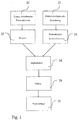
- Fig. 1 shows a flow chart, which the inventive Production order in the production of personalized chip cards indicates.
- the integrated circuits or Modules that contain the integrated circuits in one Multi-contact station subjected to an entrance test. After that If necessary, the chips recognized as good are initialized and personalized. When personalizing the individual chips card-specific data records in a specified order assigned. Personalization after the test and initialization ensures that the error rate in personalization caused by Chip defects or contact problems is caused is very low.
- the integrated circuits or modules are opened the carrier tape on which they are arranged for transport is punched out.
- an adjustment criterion can advantageously be made from the Can be read to ensure synchronicity in the event of a fault Restore personalization of the chip modules and card body.
- This code will be used in the next step 23 for card body personalization evaluated so that the code of the workpiece carrier assigned data record for the personalization of the card body can be used.
- the chip card additional Contains magnetic stripes preferably takes place after the chip personalization in the order of the successfully personalized chips the magnetic stripe coding.
- the magnetic stripe coding will preferably carried out before optical coding.
- Step 25 then sees, for example, with the help of the read one Workpiece carrier codes before a check with which are determined can whether the personalized modules the personalized card bodies were assigned correctly or the chip was not assigned during implantation was damaged.
- step 26 the cards are given in a predetermined format Order placed in a magazine.
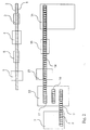
- Fig. 2 shows a device with which the The inventive method can be used. It will be a coil-shaped rolled carrier tape 1 on which the integrated Circuits 2 are preferably arranged in two rows for transporting the Circuits or the modules used. In station 3 it is checked whether the carrier tape is correctly equipped with the modules. Furthermore, in a bad hole detection was carried out at this station, i.e. it will checks whether the chips or modules have already been tested were marked as incorrect to be corrected in the later Personalization.
- the modules are first one Functional test. A predetermined number can be stored in this station modules can be contacted and processed at the same time. As well-tested circuits are then initialized if necessary, whereupon the successfully initialized modules with the individual cards Data records, i.e. be personalized.
- the personalized modules 2 become optional arranged reading station 5 supplied with the freedom from errors is checked again before the modules in the punching device 6 are punched out and passed on to the implantation device 10.
- the virgin card bodies from magazine 7 on the coded workpiece carrier 9 to the personalization device 12 transported. On the way there can be a test device if necessary be arranged with which the card body e.g. optically examined for errors become.
- the card bodies are in the personalization device 12 individually or in a group 10 according to the Workpiece carrier coding personalized with the assigned data record.
- the workpiece carriers are personalized with the Card bodies guided on the carrier tape 11 and the Implantation device 13 supplied.
- the completed ones Chip cards 14 are used for the final check for the correct one Complete personalization of a checking device 15, in which reads the data stored in the chip and with the data on the Card body applied personalization data and / or the Workpiece carrier code can be compared.
- a checking device 15 in which reads the data stored in the chip and with the data on the Card body applied personalization data and / or the Workpiece carrier code can be compared.
- To check the data can for example an image acquisition unit with text recognition or Barcode reading to record the information on the card surface Data are used.
- Faulty cards are sorted out by a unit 16 and it is post-personalization is initialized for the data record concerned.
- the cards tested are fed to a sorting buffer 17, of the completed smart cards in one through the records predefined order in a magazine.
- the finished chip card also contain a magnetic strip should, a device for Personalization of the magnetic stripe can be arranged.
Landscapes
- Engineering & Computer Science (AREA)
- Computer Hardware Design (AREA)
- Microelectronics & Electronic Packaging (AREA)
- Physics & Mathematics (AREA)
- General Physics & Mathematics (AREA)
- Theoretical Computer Science (AREA)
- Credit Cards Or The Like (AREA)
- Encapsulation Of And Coatings For Semiconductor Or Solid State Devices (AREA)
- Die Bonding (AREA)
Applications Claiming Priority (2)
| Application Number | Priority Date | Filing Date | Title |
|---|---|---|---|
| DE19858343 | 1998-12-17 | ||
| DE19858343A DE19858343A1 (de) | 1998-12-17 | 1998-12-17 | Verfahren und Vorrichtung zum Herstellen von personalisierten Chipkarten |
Publications (3)
| Publication Number | Publication Date |
|---|---|
| EP1011071A2 true EP1011071A2 (fr) | 2000-06-21 |
| EP1011071A3 EP1011071A3 (fr) | 2004-03-10 |
| EP1011071B1 EP1011071B1 (fr) | 2009-03-11 |
Family
ID=7891488
Family Applications (1)
| Application Number | Title | Priority Date | Filing Date |
|---|---|---|---|
| EP99124007A Expired - Lifetime EP1011071B1 (fr) | 1998-12-17 | 1999-12-08 | Méthode et dispositif pour la fabrication de cartes à puce personnalisées |
Country Status (5)
| Country | Link |
|---|---|
| US (2) | US6484935B1 (fr) |
| EP (1) | EP1011071B1 (fr) |
| JP (1) | JP4607273B2 (fr) |
| AT (1) | ATE425511T1 (fr) |
| DE (2) | DE19858343A1 (fr) |
Cited By (9)
| Publication number | Priority date | Publication date | Assignee | Title |
|---|---|---|---|---|
| WO2001097169A1 (fr) * | 2000-06-13 | 2001-12-20 | Nedcard B.V. | Procede de traitement de microcircuits installes sur un ruban porteur |
| EP1187065A2 (fr) * | 2000-09-05 | 2002-03-13 | ACG Aktiengesellschaft für Chipkarten und Informationssysteme | Procédé de fabrication en série de puces, en particulier pour des cartes SIM |
| EP1187064A1 (fr) * | 2000-09-05 | 2002-03-13 | ACG Aktiengesellschaft für Chipkarten und Informationssysteme | Procédé de fabrication en série de cartes à puce, notamment de cartes SIM |
| EP1187063A1 (fr) * | 2000-09-05 | 2002-03-13 | ACG Aktiengesellschaft für Chipkarten und Informationssysteme | Procédé de fabrication en série de cartes à puce, notamment de cartes SIM |
| FR2822987A1 (fr) * | 2001-04-03 | 2002-10-04 | Cybernetix | Procede de manipulation et de traitement des cartes dans une machine lineaire et cartes ainsi obtenues |
| FR2822989A1 (fr) * | 2001-04-03 | 2002-10-04 | Cybernetix | Machine lineaire de traitement de cartes, notamment a circuit integre |
| WO2007124939A1 (fr) * | 2006-04-28 | 2007-11-08 | Giesecke & Devrient Gmbh | Procede et dispositif pour la personnalisation de supports de donnees portables |
| FR2952213A1 (fr) * | 2009-11-04 | 2011-05-06 | Nbs Technologies | Machine lineaire de traitement individuel d'objets et procede de mise en oeuvre |
| CN101479744B (zh) * | 2006-04-28 | 2013-05-22 | 德国捷德有限公司 | 个性化便携式数据载体的方法和装置 |
Families Citing this family (13)
| Publication number | Priority date | Publication date | Assignee | Title |
|---|---|---|---|---|
| FR2847363B1 (fr) * | 2002-11-15 | 2005-01-07 | Smartware | Machine a haute cadence de personnalisation de module a circuit integre |
| FR2853434B1 (fr) * | 2003-04-03 | 2005-07-01 | Oberthur Card Syst Sa | Carte a microcircuit fixee sur un support adaptateur, support de carte et procede de fabrication |
| FR2862409B1 (fr) * | 2003-11-17 | 2006-04-14 | Datacard Inc | Element d'adaptation pour supports electroniques programmables |
| DE102004028218B4 (de) * | 2004-06-09 | 2006-06-29 | Giesecke & Devrient Gmbh | Verfahren zur Herstellung eines tragbaren Datenträgers |
| DE102004058020A1 (de) * | 2004-12-01 | 2006-06-08 | Siemens Ag | Verfahren zur Personalisierung von Chipkarten |
| US7963438B2 (en) * | 2005-11-10 | 2011-06-21 | Magtek, Inc. | System and method for personalizing a card |
| DE102006020227A1 (de) * | 2006-05-02 | 2007-11-08 | Giesecke & Devrient Gmbh | Verfahren zur Personalisierung elektronischer Datenträger und Personalisierungsautomat dafür |
| DE102006034375A1 (de) * | 2006-07-25 | 2008-01-31 | Giesecke & Devrient Gmbh | Personalisierung von tragbaren Datenträgern |
| FR2906952B1 (fr) * | 2006-10-05 | 2009-02-27 | Inside Contactless Sa | Procede d'authentification mutuelle entre une interface de communication et un processeur hote d'un chipset nfc. |
| FR2918196B1 (fr) * | 2007-06-27 | 2009-08-14 | Datacard Corp | Machine pour personnaliser des cartes a puce avec une cadence elevee. |
| FR2953617B1 (fr) * | 2009-12-03 | 2012-01-20 | Herve Mongin | Machine de personnalisation electrique et graphique d'objets electroniques portatifs |
| ITUB20155233A1 (it) * | 2015-10-30 | 2017-04-30 | Automation 4 Industiral Solutions S R L | Metodo di impianto per la realizzazione di dispositivi rfid |
| CN111307833B (zh) * | 2019-11-25 | 2023-05-23 | 新恒汇电子股份有限公司 | 一种智能卡芯片贴装视觉检测方法 |
Citations (2)
| Publication number | Priority date | Publication date | Assignee | Title |
|---|---|---|---|---|
| DE19614808A1 (de) * | 1996-04-15 | 1997-10-16 | Giesecke & Devrient Gmbh | Verfahren zur Herstellung von Karten |
| WO1998018106A1 (fr) * | 1996-10-17 | 1998-04-30 | Gkard S.A.S. | Procede et installation pour realiser un titre d'usager personnalise infalsifiable |
Family Cites Families (19)
| Publication number | Priority date | Publication date | Assignee | Title |
|---|---|---|---|---|
| US4222516A (en) * | 1975-12-31 | 1980-09-16 | Compagnie Internationale Pour L'informatique Cii-Honeywell Bull | Standardized information card |
| DE3019207A1 (de) * | 1980-05-20 | 1981-11-26 | GAO Gesellschaft für Automation und Organisation mbH, 8000 München | Traegerelement fuer einen ic-chip |
| DE3123198C2 (de) * | 1980-12-08 | 1993-10-07 | Gao Ges Automation Org | Trägerelemente für einen IC-Baustein |
| US4889980A (en) * | 1985-07-10 | 1989-12-26 | Casio Computer Co., Ltd. | Electronic memory card and method of manufacturing same |
| US4874935A (en) * | 1986-03-10 | 1989-10-17 | Data Card Coprporation | Smart card apparatus and method of programming same |
| AU7129487A (en) * | 1986-03-10 | 1987-09-28 | Data Card Corporation | Smart card apparatus and method of programming same |
| JPS6356785A (ja) | 1986-08-28 | 1988-03-11 | Toshiba Corp | 携帯可能記憶媒体処理装置 |
| US4827425A (en) * | 1986-10-31 | 1989-05-02 | Thorn Emi Malco, Incorporated | System for personalization of integrated circuit microchip cards |
| JPH0196781A (ja) * | 1987-10-09 | 1989-04-14 | Toshiba Corp | 携帯可能記憶媒体処理装置 |
| US4825054A (en) * | 1988-02-16 | 1989-04-25 | Datacard Corporation | Method and apparatus for parallel integrated circuit card initialization and embossing |
| JP2808303B2 (ja) * | 1989-05-10 | 1998-10-08 | 大日本印刷株式会社 | Icデバイステスト装置 |
| US5049728A (en) * | 1990-04-04 | 1991-09-17 | Rovin George H | IC card system with removable IC modules |
| JPH04179595A (ja) * | 1990-11-14 | 1992-06-26 | Dainippon Printing Co Ltd | Icカードおよびその製造方法 |
| DE4421607A1 (de) * | 1994-06-21 | 1996-01-04 | Giesecke & Devrient Gmbh | Verfahren zur Herstellung von Datenträgern |
| US5680936A (en) | 1995-03-14 | 1997-10-28 | Automated Technologies Industries, Inc. | Printed circuit board sorting device |
| DE19544944A1 (de) * | 1995-12-01 | 1997-06-05 | Weisser Otto Marina | Speicherkarte zur Aufnahme unpersonalisierter Daten |
| US5889941A (en) * | 1996-04-15 | 1999-03-30 | Ubiq Inc. | System and apparatus for smart card personalization |
| DE19615980C2 (de) * | 1996-04-22 | 1999-02-04 | Fraunhofer Ges Forschung | Datenträgerkarte mit einem Kartenzwischenerzeugnis |
| US6193163B1 (en) * | 1998-08-31 | 2001-02-27 | The Standard Register Company | Smart card with replaceable chip |
-
1998
- 1998-12-17 DE DE19858343A patent/DE19858343A1/de not_active Withdrawn
-
1999
- 1999-12-08 DE DE59914976T patent/DE59914976D1/de not_active Expired - Lifetime
- 1999-12-08 AT AT99124007T patent/ATE425511T1/de not_active IP Right Cessation
- 1999-12-08 EP EP99124007A patent/EP1011071B1/fr not_active Expired - Lifetime
- 1999-12-17 JP JP35949499A patent/JP4607273B2/ja not_active Expired - Fee Related
- 1999-12-17 US US09/466,221 patent/US6484935B1/en not_active Expired - Fee Related
-
2002
- 2002-07-26 US US10/205,221 patent/US6622910B2/en not_active Expired - Fee Related
Patent Citations (2)
| Publication number | Priority date | Publication date | Assignee | Title |
|---|---|---|---|---|
| DE19614808A1 (de) * | 1996-04-15 | 1997-10-16 | Giesecke & Devrient Gmbh | Verfahren zur Herstellung von Karten |
| WO1998018106A1 (fr) * | 1996-10-17 | 1998-04-30 | Gkard S.A.S. | Procede et installation pour realiser un titre d'usager personnalise infalsifiable |
Non-Patent Citations (1)
| Title |
|---|
| LENDER F: "HERSTELLUNG, PERSONALISIERUNG UND VERSAND VON CHIPKARTEN - EIN UEBERBLICK" IT + TI INFORMATIONSTECHNIK UND TECHNISCHE INFORMATIK, OLDENBOURG VERLAG. MUNCHEN, DE, Bd. 39, Nr. 5, 1. Oktober 1997 (1997-10-01), Seiten 7-13, XP000702135 ISSN: 0944-2774 * |
Cited By (14)
| Publication number | Priority date | Publication date | Assignee | Title |
|---|---|---|---|---|
| WO2001097169A1 (fr) * | 2000-06-13 | 2001-12-20 | Nedcard B.V. | Procede de traitement de microcircuits installes sur un ruban porteur |
| EP1187065A2 (fr) * | 2000-09-05 | 2002-03-13 | ACG Aktiengesellschaft für Chipkarten und Informationssysteme | Procédé de fabrication en série de puces, en particulier pour des cartes SIM |
| EP1187064A1 (fr) * | 2000-09-05 | 2002-03-13 | ACG Aktiengesellschaft für Chipkarten und Informationssysteme | Procédé de fabrication en série de cartes à puce, notamment de cartes SIM |
| EP1187063A1 (fr) * | 2000-09-05 | 2002-03-13 | ACG Aktiengesellschaft für Chipkarten und Informationssysteme | Procédé de fabrication en série de cartes à puce, notamment de cartes SIM |
| WO2002021434A1 (fr) * | 2000-09-05 | 2002-03-14 | Acg Advanced Component Group Aktiengesellschaft | Procede de fabrication de puces en serie, notamment pour des cartes sim |
| EP1187065A3 (fr) * | 2000-09-05 | 2002-07-31 | ACG Aktiengesellschaft für Chipkarten und Informationssysteme | Procédé de fabrication en série de puces, en particulier pour des cartes SIM |
| FR2822987A1 (fr) * | 2001-04-03 | 2002-10-04 | Cybernetix | Procede de manipulation et de traitement des cartes dans une machine lineaire et cartes ainsi obtenues |
| FR2822989A1 (fr) * | 2001-04-03 | 2002-10-04 | Cybernetix | Machine lineaire de traitement de cartes, notamment a circuit integre |
| WO2002082360A1 (fr) * | 2001-04-03 | 2002-10-17 | Cybernetix S.A. | Machine lineaire de traitement de cartes, notamment a circuit integre |
| WO2002082370A1 (fr) * | 2001-04-03 | 2002-10-17 | Cybernetix | Procede de manipulation et de traitement des cartes dans une machine lineaire |
| WO2007124939A1 (fr) * | 2006-04-28 | 2007-11-08 | Giesecke & Devrient Gmbh | Procede et dispositif pour la personnalisation de supports de donnees portables |
| CN101479744B (zh) * | 2006-04-28 | 2013-05-22 | 德国捷德有限公司 | 个性化便携式数据载体的方法和装置 |
| US8544733B2 (en) | 2006-04-28 | 2013-10-01 | Giesecke & Devrient Gmbh | Method and apparatus for personalizing portable data storage media |
| FR2952213A1 (fr) * | 2009-11-04 | 2011-05-06 | Nbs Technologies | Machine lineaire de traitement individuel d'objets et procede de mise en oeuvre |
Also Published As
| Publication number | Publication date |
|---|---|
| DE19858343A1 (de) | 2000-06-21 |
| JP4607273B2 (ja) | 2011-01-05 |
| US6622910B2 (en) | 2003-09-23 |
| US6484935B1 (en) | 2002-11-26 |
| US20020179702A1 (en) | 2002-12-05 |
| DE59914976D1 (de) | 2009-04-23 |
| ATE425511T1 (de) | 2009-03-15 |
| JP2000200336A (ja) | 2000-07-18 |
| EP1011071B1 (fr) | 2009-03-11 |
| EP1011071A3 (fr) | 2004-03-10 |
Similar Documents
| Publication | Publication Date | Title |
|---|---|---|
| EP1011071B1 (fr) | Méthode et dispositif pour la fabrication de cartes à puce personnalisées | |
| DE3049607C3 (de) | Verfahren zur Herstellung von Ausweiskarten und Vorrichtung zu dessen Durchführung | |
| EP0453737A1 (fr) | Probe pour cartes de crédit avec puce semi-conductrice incorporée | |
| DE3917876A1 (de) | System zum beladen eines chirurgischen instrumentensets | |
| WO2007124939A1 (fr) | Procede et dispositif pour la personnalisation de supports de donnees portables | |
| US6431453B1 (en) | Automated card insertion system with card multireader and method | |
| EP1488374B1 (fr) | Procede et dispositif pour manipuler des cartes | |
| EP0863483B1 (fr) | Installation pour le traitement de cartes à puce et/ou magnétiques | |
| EP1001885B1 (fr) | Procede et dispositif pour reunir et assembler des cartes en plastique et des supports de carte | |
| DE19508283C1 (de) | Verfahren und Vorrichtung zum Zusammenführen und Verbinden von Kunststoffkarten und bedruckten Kartenträgern | |
| DE10250653B4 (de) | Verfahren und Vorrichtung zum Bereitstellen eines Kartenträgers für eine Zusammenführung mit einer Karte | |
| DE102007002289A1 (de) | Handelbares Paket zur Aufnahme eines tragbaren Datenträgers und geeigneter tragbarer Datenträger | |
| DE19734119C1 (de) | Verfahren zur Bearbeitung von Karten in Verbindung mit Kartenbearbeitungsanlagen | |
| DE19922063A1 (de) | Adapterkarte und Kommunikationsvorrichtung | |
| DE102011112214B4 (de) | Verfahren und Vorrichtung zum Sortieren von Identifikationsgegenständen | |
| WO2002087302A1 (fr) | Dispositif de caracterisation des stocks de composants, et procede utilisant ce dispositif | |
| WO2019145319A1 (fr) | Dispositif et procédé pour le codage de transpondeurs rf | |
| EP1261936B1 (fr) | Procede et dispositif de personnalisation de cartes a puce | |
| EP1187065A2 (fr) | Procédé de fabrication en série de puces, en particulier pour des cartes SIM | |
| EP1035505A2 (fr) | Carte de visite électronique | |
| DE4415667A1 (de) | Verfahren zur Bildung einer Versandeinheit aus Brief und Chipkarte sowie Vorrichtung zur Durchführung des Verfahrens | |
| DE69723600T2 (de) | Verfahren und Vorrichtung zur Kontrolle von Kartenzuführung | |
| DE10141095C2 (de) | Verfahren zur Verbesserung des Lesens von Magnetspurdaten beim Einführen einer Karte in einen DIP Leser | |
| DE102006024106A1 (de) | Verfahren zur Bearbeitung von tragbaren Datenträgern | |
| DD224138A1 (de) | Kartenfoermiger aufzeichnungstraeger |
Legal Events
| Date | Code | Title | Description |
|---|---|---|---|
| PUAI | Public reference made under article 153(3) epc to a published international application that has entered the european phase |
Free format text: ORIGINAL CODE: 0009012 |
|
| AK | Designated contracting states |
Kind code of ref document: A2 Designated state(s): AT BE CH CY DE DK ES FI FR GB GR IE IT LI LU MC NL PT SE |
|
| AX | Request for extension of the european patent |
Free format text: AL;LT;LV;MK;RO;SI |
|
| PUAL | Search report despatched |
Free format text: ORIGINAL CODE: 0009013 |
|
| RIC1 | Information provided on ipc code assigned before grant |
Ipc: 7G 06K 19/07 B Ipc: 7G 06K 19/077 A |
|
| AK | Designated contracting states |
Kind code of ref document: A3 Designated state(s): AT BE CH CY DE DK ES FI FR GB GR IE IT LI LU MC NL PT SE |
|
| AX | Request for extension of the european patent |
Extension state: AL LT LV MK RO SI |
|
| 17P | Request for examination filed |
Effective date: 20040910 |
|
| AKX | Designation fees paid |
Designated state(s): AT BE CH CY DE DK ES FI FR GB GR IE IT LI LU MC NL PT SE |
|
| AXX | Extension fees paid |
Extension state: SI Payment date: 20040910 Extension state: RO Payment date: 20040910 Extension state: MK Payment date: 20040910 Extension state: LV Payment date: 20040910 Extension state: LT Payment date: 20040910 Extension state: AL Payment date: 20040910 |
|
| GRAP | Despatch of communication of intention to grant a patent |
Free format text: ORIGINAL CODE: EPIDOSNIGR1 |
|
| GRAS | Grant fee paid |
Free format text: ORIGINAL CODE: EPIDOSNIGR3 |
|
| GRAA | (expected) grant |
Free format text: ORIGINAL CODE: 0009210 |
|
| AK | Designated contracting states |
Kind code of ref document: B1 Designated state(s): AT BE CH CY DE DK ES FI FR GB GR IE IT LI LU MC NL PT SE |
|
| AX | Request for extension of the european patent |
Extension state: AL LT LV MK RO SI |
|
| REG | Reference to a national code |
Ref country code: GB Ref legal event code: FG4D Free format text: NOT ENGLISH |
|
| REG | Reference to a national code |
Ref country code: CH Ref legal event code: EP |
|
| REG | Reference to a national code |
Ref country code: IE Ref legal event code: FG4D Free format text: LANGUAGE OF EP DOCUMENT: GERMAN |
|
| REF | Corresponds to: |
Ref document number: 59914976 Country of ref document: DE Date of ref document: 20090423 Kind code of ref document: P |
|
| PG25 | Lapsed in a contracting state [announced via postgrant information from national office to epo] |
Ref country code: NL Free format text: LAPSE BECAUSE OF FAILURE TO SUBMIT A TRANSLATION OF THE DESCRIPTION OR TO PAY THE FEE WITHIN THE PRESCRIBED TIME-LIMIT Effective date: 20090311 Ref country code: FI Free format text: LAPSE BECAUSE OF FAILURE TO SUBMIT A TRANSLATION OF THE DESCRIPTION OR TO PAY THE FEE WITHIN THE PRESCRIBED TIME-LIMIT Effective date: 20090311 |
|
| NLV1 | Nl: lapsed or annulled due to failure to fulfill the requirements of art. 29p and 29m of the patents act | ||
| LTIE | Lt: invalidation of european patent or patent extension |
Effective date: 20090311 |
|
| PG25 | Lapsed in a contracting state [announced via postgrant information from national office to epo] |
Ref country code: SE Free format text: LAPSE BECAUSE OF FAILURE TO SUBMIT A TRANSLATION OF THE DESCRIPTION OR TO PAY THE FEE WITHIN THE PRESCRIBED TIME-LIMIT Effective date: 20090611 |
|
| REG | Reference to a national code |
Ref country code: IE Ref legal event code: FD4D |
|
| PG25 | Lapsed in a contracting state [announced via postgrant information from national office to epo] |
Ref country code: PT Free format text: LAPSE BECAUSE OF FAILURE TO SUBMIT A TRANSLATION OF THE DESCRIPTION OR TO PAY THE FEE WITHIN THE PRESCRIBED TIME-LIMIT Effective date: 20090824 Ref country code: IE Free format text: LAPSE BECAUSE OF FAILURE TO SUBMIT A TRANSLATION OF THE DESCRIPTION OR TO PAY THE FEE WITHIN THE PRESCRIBED TIME-LIMIT Effective date: 20090311 Ref country code: ES Free format text: LAPSE BECAUSE OF FAILURE TO SUBMIT A TRANSLATION OF THE DESCRIPTION OR TO PAY THE FEE WITHIN THE PRESCRIBED TIME-LIMIT Effective date: 20090622 |
|
| PLBE | No opposition filed within time limit |
Free format text: ORIGINAL CODE: 0009261 |
|
| STAA | Information on the status of an ep patent application or granted ep patent |
Free format text: STATUS: NO OPPOSITION FILED WITHIN TIME LIMIT |
|
| PG25 | Lapsed in a contracting state [announced via postgrant information from national office to epo] |
Ref country code: DK Free format text: LAPSE BECAUSE OF FAILURE TO SUBMIT A TRANSLATION OF THE DESCRIPTION OR TO PAY THE FEE WITHIN THE PRESCRIBED TIME-LIMIT Effective date: 20090311 |
|
| 26N | No opposition filed |
Effective date: 20091214 |
|
| BERE | Be: lapsed |
Owner name: GIESECKE & DEVRIENT G.M.B.H. Effective date: 20091231 |
|
| PG25 | Lapsed in a contracting state [announced via postgrant information from national office to epo] |
Ref country code: MC Free format text: LAPSE BECAUSE OF NON-PAYMENT OF DUE FEES Effective date: 20100701 |
|
| REG | Reference to a national code |
Ref country code: CH Ref legal event code: PL |
|
| GBPC | Gb: european patent ceased through non-payment of renewal fee |
Effective date: 20091208 |
|
| PG25 | Lapsed in a contracting state [announced via postgrant information from national office to epo] |
Ref country code: LI Free format text: LAPSE BECAUSE OF NON-PAYMENT OF DUE FEES Effective date: 20091231 Ref country code: GR Free format text: LAPSE BECAUSE OF FAILURE TO SUBMIT A TRANSLATION OF THE DESCRIPTION OR TO PAY THE FEE WITHIN THE PRESCRIBED TIME-LIMIT Effective date: 20090612 Ref country code: CH Free format text: LAPSE BECAUSE OF NON-PAYMENT OF DUE FEES Effective date: 20091231 Ref country code: BE Free format text: LAPSE BECAUSE OF NON-PAYMENT OF DUE FEES Effective date: 20091231 |
|
| PG25 | Lapsed in a contracting state [announced via postgrant information from national office to epo] |
Ref country code: GB Free format text: LAPSE BECAUSE OF NON-PAYMENT OF DUE FEES Effective date: 20091208 |
|
| PG25 | Lapsed in a contracting state [announced via postgrant information from national office to epo] |
Ref country code: IT Free format text: LAPSE BECAUSE OF FAILURE TO SUBMIT A TRANSLATION OF THE DESCRIPTION OR TO PAY THE FEE WITHIN THE PRESCRIBED TIME-LIMIT Effective date: 20090311 |
|
| PG25 | Lapsed in a contracting state [announced via postgrant information from national office to epo] |
Ref country code: LU Free format text: LAPSE BECAUSE OF NON-PAYMENT OF DUE FEES Effective date: 20091208 |
|
| PG25 | Lapsed in a contracting state [announced via postgrant information from national office to epo] |
Ref country code: AT Free format text: LAPSE BECAUSE OF NON-PAYMENT OF DUE FEES Effective date: 20091208 |
|
| PG25 | Lapsed in a contracting state [announced via postgrant information from national office to epo] |
Ref country code: CY Free format text: LAPSE BECAUSE OF FAILURE TO SUBMIT A TRANSLATION OF THE DESCRIPTION OR TO PAY THE FEE WITHIN THE PRESCRIBED TIME-LIMIT Effective date: 20090311 |
|
| PGFP | Annual fee paid to national office [announced via postgrant information from national office to epo] |
Ref country code: DE Payment date: 20121231 Year of fee payment: 14 Ref country code: FR Payment date: 20130123 Year of fee payment: 14 |
|
| REG | Reference to a national code |
Ref country code: DE Ref legal event code: R082 Ref document number: 59914976 Country of ref document: DE |
|
| REG | Reference to a national code |
Ref country code: DE Ref legal event code: R119 Ref document number: 59914976 Country of ref document: DE |
|
| REG | Reference to a national code |
Ref country code: DE Ref legal event code: R119 Ref document number: 59914976 Country of ref document: DE Effective date: 20140701 |
|
| REG | Reference to a national code |
Ref country code: FR Ref legal event code: ST Effective date: 20140829 |
|
| PG25 | Lapsed in a contracting state [announced via postgrant information from national office to epo] |
Ref country code: DE Free format text: LAPSE BECAUSE OF NON-PAYMENT OF DUE FEES Effective date: 20140701 |
|
| PG25 | Lapsed in a contracting state [announced via postgrant information from national office to epo] |
Ref country code: FR Free format text: LAPSE BECAUSE OF NON-PAYMENT OF DUE FEES Effective date: 20131231 |