EP1008169B1 - Realisation de microstructures ou de nanostructures sur un support - Google Patents
Realisation de microstructures ou de nanostructures sur un support Download PDFInfo
- Publication number
- EP1008169B1 EP1008169B1 EP98939717A EP98939717A EP1008169B1 EP 1008169 B1 EP1008169 B1 EP 1008169B1 EP 98939717 A EP98939717 A EP 98939717A EP 98939717 A EP98939717 A EP 98939717A EP 1008169 B1 EP1008169 B1 EP 1008169B1
- Authority
- EP
- European Patent Office
- Prior art keywords
- crystalline
- lattice
- wafer
- defects
- wafers
- Prior art date
- Legal status (The legal status is an assumption and is not a legal conclusion. Google has not performed a legal analysis and makes no representation as to the accuracy of the status listed.)
- Expired - Lifetime
Links
Images
Classifications
-
- H—ELECTRICITY
- H10—SEMICONDUCTOR DEVICES; ELECTRIC SOLID-STATE DEVICES NOT OTHERWISE PROVIDED FOR
- H10P—GENERIC PROCESSES OR APPARATUS FOR THE MANUFACTURE OR TREATMENT OF DEVICES COVERED BY CLASS H10
- H10P50/00—Etching of wafers, substrates or parts of devices
-
- B—PERFORMING OPERATIONS; TRANSPORTING
- B82—NANOTECHNOLOGY
- B82Y—SPECIFIC USES OR APPLICATIONS OF NANOSTRUCTURES; MEASUREMENT OR ANALYSIS OF NANOSTRUCTURES; MANUFACTURE OR TREATMENT OF NANOSTRUCTURES
- B82Y10/00—Nanotechnology for information processing, storage or transmission, e.g. quantum computing or single electron logic
-
- B—PERFORMING OPERATIONS; TRANSPORTING
- B82—NANOTECHNOLOGY
- B82Y—SPECIFIC USES OR APPLICATIONS OF NANOSTRUCTURES; MEASUREMENT OR ANALYSIS OF NANOSTRUCTURES; MANUFACTURE OR TREATMENT OF NANOSTRUCTURES
- B82Y30/00—Nanotechnology for materials or surface science, e.g. nanocomposites
-
- H—ELECTRICITY
- H10—SEMICONDUCTOR DEVICES; ELECTRIC SOLID-STATE DEVICES NOT OTHERWISE PROVIDED FOR
- H10P—GENERIC PROCESSES OR APPARATUS FOR THE MANUFACTURE OR TREATMENT OF DEVICES COVERED BY CLASS H10
- H10P10/00—Bonding of wafers, substrates or parts of devices
- H10P10/12—Bonding of semiconductor wafers or semiconductor substrates to semiconductor wafers or semiconductor substrates
-
- H—ELECTRICITY
- H10—SEMICONDUCTOR DEVICES; ELECTRIC SOLID-STATE DEVICES NOT OTHERWISE PROVIDED FOR
- H10P—GENERIC PROCESSES OR APPARATUS FOR THE MANUFACTURE OR TREATMENT OF DEVICES COVERED BY CLASS H10
- H10P90/00—Preparation of wafers not covered by a single main group of this subclass, e.g. wafer reinforcement
Definitions
- the present invention relates to the production of microstructures or nanostructures on a support.
- microstructures and the nanostructures for still smaller dimensions, are in the form of a network of microvolumes of material obtained on the surface of a support.
- microvolume means, for example, volumes of parallelepiped shape, preferably smaller than one micrometer.
- microstructures in semiconductor material and in particular in silicon, AsGa, III-V compounds and SiC.
- conducting materials such as metals, and dielectric materials such as SiO 2 .
- micro- or nanostructures are intended for the production of electronic, optical or optoelectronic devices.
- this type of structure allows the realization of a quantum dot array (called “quantum dots” in the English terminology), or electronic devices called mono-electron or Coulomb blocking (“Coulomb blockade”) or else light emitting devices.
- microstructures When we want to make microstructures, we use the techniques today in the field of microelectronics. In particular, the principles of lithography combined with dry or wet etching, ion implantation, deposition and heat treatment operations are used. For example, if one wants to make a square network of parallelepiped microvolumes monocrystalline silicon, each microvolume having 1 micron side to 0.2 microns thick, microvolumes being spaced from each other by 0.5 microns, can start from a SSI (Silicon On Insulator) wafer having a 0.2 micron thick monocrystalline silicon layer.
- SSI Silicon On Insulator
- a layer of photosensitive resin is applied to the silicon layer of the wafer and is insulated by means of an Electron Beam Pattern Generator ("Electron Beam Pattern Generator") so as to inscribe in the resin a matrix of rows and columns 0.5 ⁇ m wide representing the spaces between the microvolumes.
- the development of the resin releases the exposed parts, exposing the silicon layer corresponding to the array of rows and columns.
- the wafer is then subjected to a plasma etching treatment selectively attacking the silicon with respect to the resin. The etching process ends when the underlying silica layer is reached.
- an array of microvolumes each having 1 ⁇ m ⁇ 1 ⁇ m ⁇ 0.2 ⁇ m in size and spaced 0.5 ⁇ m apart is obtained. If necessary, the spaces between microvolumes can then be filled by a dielectric layer such as SiO 2 , or by using a thermal oxidation process or a CVD type deposit.
- microstructures with microvolumes of much smaller dimensions for example a few tens of nanometers
- condensation nuclei randomly distributed on the surface can be obtained.
- microstructures are multiple and depend on the particular properties of each. These properties are related to a size effect on the electronic states of carriers in these materials, surface effects, interface effects, the existence or not of intergranular phases, etc.
- a particular application is the production of light emitters, in particular from materials such as silicon which, in the solid monocrystalline state, are not emitters (see the article by T. KOMOKA already cited).
- Another application is the realization of electronic devices based on the quantum confinement of electronic carriers in microvolumes of the structure or Coulomb blocking effects. This application is described in the article " Modeling the Multiplicity of Conductance Structures in Clusters of Silicon Quantum Dots by DW BOERINGER and R. TSU, published in Mat. Res, Soc Symp, Proc Vol 358, pp. 569-574, 1995. , Materials Research Society.
- the present invention has been designed to allow the production of microstructures that may include microvolumes of dimensions significantly smaller than microvolumes currently achievable, for example a few tens of nm, economically and over large areas.
- these microstructures are organized according to a predetermined plan instead of being randomly distributed.
- the invention proposes a process for producing micro- or nanostructures, which applies to crystalline materials, whether they are semiconductors, conductors or dielectrics.
- the disagree parameter can be constituted by a given angle of offset in rotation of the crystal lattices presented by said faces.
- the network of defects obtained, called “twist” is a network of dislocations to character screws.
- the disagreement parameter can also be constituted by a difference in crystal lattice parameter between the crystalline materials of the faces of the wafers put in contact with the resulting defect network is called "misfit".
- the detuning parameter can also be constituted by a determined angle according to which the face of at least one of the platelets is offset with respect to the single crystallographic plane of direction corresponding to this face.
- the disoriented crystalline faces (one or both) with respect to a simple crystallographic plane are called vicinal.
- the fault network is called "miscut”.
- mismatch parameters are possible, for example by gluing two different materials and offset in rotation. Several networks are then formed.
- the contacting may preferably be hydrophobic type, that is to say, direct bonding of the faces of said wafers. It may be of the hydrophilic type, that is to say involving a thin intermediate layer, for example an oxide layer formed naturally on one face of a wafer or on the faces of the wafers.
- the method also comprises at least one heat treatment step intended either to complete the formation of the crystal defect network and / or the constraint network if the contacting is insufficient to complete it, or to complete it completely.
- this treatment may be able to reinforce the interatomic bonds between the faces of the platelets put in contact.
- This heat treatment can be performed before or after the thinning step.
- the thinning step may be carried out using a technique chosen from grinding, mechanical abrasion or chemical abrasion.
- the thinning step may also be carried out by cleaving one of the platelets which, before the contacting step has been subjected, through its contacting face, to an ion implantation step intended to create, at a determined depth and corresponding to the desired thinning, a layer of microcavities capable of generating a cleavage plane during a subsequent heat treatment step.
- the ion implantation can be carried out by means of hydrogen ions.
- the thinning step it can be provided at least one heat treatment step simultaneously making it possible to complete or complete the formation of the lattice of crystalline defects and / or the network of stresses, to reinforce the interatomic bonds between the faces of the platelets contacted and generate the cleavage plane.
- the micro- or nanostructure after the thinning step, it may be provided a step of selectively treating the lattice of crystalline defects and / or the stress network with respect to said crystalline zone .
- This selective treatment step may consist of conductive crystalline defects and / or the network of stresses so that said crystalline zone forms crystalline pads electrically connected to each other. In this case, it is possible to carry out a phosphorus diffusion which diffuses preferentially at the level of the crystalline defects.
- the selective treatment step may also consist of electrical insulation so that said crystalline zone forms crystalline pads electrically insulated from each other.
- the chemical etching may be preceded by a crystalline defects decoration phase and / or the stress network by precipitation of metal impurities or dopants.
- the network of defects produced by the techniques indicated above extends a small thickness on either side of the bonding surface of the two wafers.
- the stresses induced by these defects extend on each side of the interface, in the wafers, over distances of the order of magnitude of the dislocation period.
- the thinning of one of the platelets can be done by stopping the operation at a distance from the interface which is of the same order of magnitude.
- the surface stress field is nonuniform and is in the image of the underlying defect network.
- the selective treatment step can then consist in depositing, for example by epitaxy, a crystalline crystal detuned crystalline material with the crystalline material revealed by the thinning step, this deposited crystalline material forming an ordered set of islands in correspondence with the lattice of underlying crystal defects.
- the electrical isolation of the selective treatment may be of the type where electrical conduction can take place by a physical effect such as the tunnel effect or the Fowler-Nordheim effect.
- the selective treatment step can also consist in treating the crystalline defects and / or the network of stresses so that said crystalline zone forms crystalline pads connected to each other by semiconductor zones or having a potential barrier.
- the subject of the invention is also a micro- or nanostructure on a support, characterized in that it is obtained according to the method described above from platelets whose faces to be in contact are made of semiconductor materials. At least one of these faces to be contacted may be SiC or III-V semiconductor material such as AsGa or GaAlAs.
- the subject of the invention is also a micro-or nanostructure on a support, characterized in that it is obtained according to the method described above, one of the wafers consisting of a silicon-on-insulator wafer, Another wafer being made of silicon and constituting the thinned wafer, the method making it possible to obtain a micro- or nanostructure consisting of microvolumes of silicon on an insulating layer.
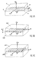
- FIGS. 1A, 1B and 1C illustrate three variants of implementation of the method according to the present invention.
- X 1 , X 2 and X 3 represent the crystallographic axes.
- the parameter that adjusts the defect density (or the average distance between defects) is the angle of rotation ⁇ existing between the crystal lattices presented by the faces contacted platelets 1 and 2.
- the parameter which regulates the density of defects (or the average distance between defects) is the angle of rotation ⁇ existing between the crystallographic planes of the plates 101 and 102 contacted.
- the parameter that adjusts the defect density (or the average distance between defects) is the mesh mismatch f 1 between the two crystalline materials of the platelets 201 and 202 contacted.
- one of the platelets can be prepared with a vicinal side shifted in the ⁇ 100> direction of 0.8 ° and glued on a non-vicinal silicon wafer (100).
- the densities of nanostructures obtained are then 2.7 ⁇ 10 15 / m 2 .
- a silicon wafer (100) is adhered to a second wafer having a SiGe layer on its surface. Since the mismatch f 1 is 2.1%, a 20 nm corner dislocation interface grating is formed. After thinning the wafer comprising the SiGe layer to approximately 10 nm, and after revelation by one of the described techniques, a density of nanostructures of the same order of magnitude as above is obtained. The bonding of a germanium wafer would produce a double clash and thus a density of nanostructures four times higher.
- Faces other than faces (100) may be used.
- the faces (111) produce at their interface hexagonal or triangular networks of dislocations.
- Faces (110) produce rectangular gratings.
- the Figure 1A shows two platelets 1 and 2 in silicon of crystallographic plane (1,0,0) when they come into contact and having plane faces, respectively 3 and 4, facing each other.
- the flat faces 3 and 4 received a surface treatment to make them hydrophobic. This will ensure an intimate and adherent contact of the faces 3 and 4.
- This surface treatment comprises a chemical cleaning step ending for example by a hydrofluoric acid etching step.
- the faces 3 and 4 are brought into contact with adhesion by molecular adhesion, for example at ambient temperature, ensuring that the crystal lattices presented by the two faces are offset relative to one another by an angle ⁇ determined, for example 0.6 °.
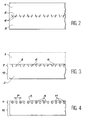
- the assembly constituted by these two inserts is then subjected to a heat treatment at a temperature of about 950 ° C for about 30 minutes. During this heat treatment, stronger and more numerous interatomic bonds are established between the two platelets. Due to the torsion angle existing between the two crystal lattices, an array of crystal defects, for example a dislocation lattice, is established in the vicinity of the interface between the two platelets, in a thin layer (a few tens to a few hundred nm) centered on the interface. This is schematically represented on the figure 2 where the reference 5 designates this interface, the crystalline defects (or dislocations) being represented under the reference 6.
- the spacing between two adjacent dislocations is a function of the ⁇ rotation angle of the crystal lattices of the two platelets.
- a surface treatment can then be implemented to differentiate, more specifically, the crystalline defects of the surrounding crystalline zone 8.
- Lateral dielectric isolation of microvolumes 9 can be performed.
- the oxide layer deposited on the microstructure 7 may be leveled, as shown in FIG. figure 4 , to keep only a deposit of insulation 11 between the microvolumes 9. In this case, we obtain a network of insulating material replacing the dislocation network.
- dislocation network conductive can also be carried out to make the dislocation network conductive, insulative, or even semiconductor depending on the intended application. This makes it possible to make the microvolumes or pads crystalline, either electrically connected to one another by conductive bonds, or electrically isolated, or connected by semiconductor zones or having a potential barrier. With regard to the electrical insulation, insulations such as electrical conduction through the insulating parts can also take place by tunnel effect for example, or by the Fowler-Nordheim effect or by any other physical effect. To make the dislocation network conductive, it is possible to carry out a phosphorus diffusion which diffuses preferentially at the level of the dislocations.
- Another possibility of carrying out the thinning step consists in applying the process described in the document FR-A-2,681,472 in order to obtain a cleavage of the wafer concerned.
- protons are implanted in this wafer to obtain a layer of microcavities at the desired depth of the face to be brought into contact. This face undergoes the cleaning and bonding treatment. The heat treatment is then applied. It allows to generate simultaneously the creation of dislocations and cleavage according to the layer of microcavities.
- One of the wafers may be an SSI (Silicon-On-Insulator) wafer called SOI ("Silicon on Insulator") in the English terminology and the other wafer may be a solid substrate. of silicon.
- SOI Silicon-On-Insulator
- the method according to the invention then provides a network of microvolumes of silicon on an insulating layer.
- the two platelets of crystalline material may be of a different nature, for example a silicon wafer and a gallium arsenide wafer, or a silicon wafer and a germanium wafer.
- platelets are not necessarily homogeneous. It suffices simply that the faces to be brought into contact are of crystalline material, the rest of the wafers may have other structures.
- the micro- or nanostructure can still be obtained from a network of constraints.
- This network of constraints can be revealed by various techniques.
- the constraint network can be revealed by deposition, by an epitaxial process (MOCVD, MBE, liquid phase epitaxy ...), on the thinned plate of a crystalline mesh detuned crystalline material.
- MOCVD epitaxial process
- MBE liquid phase epitaxy
- the preferential nucleation sites provided by the zones in compression (respectively in tension) will be favorable for the smaller (respectively larger) mesh deposits than the thinned plate.
- An ordered set of islands of size corresponding to the underlying network will thus be formed.
- This deposit can be illustrated from the variant of the process illustrated by the figure 1C .
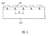
- An assembly has been prepared according to this variant, as described above, from an orientation silicon wafer (100) and a wafer comprising the SiGe layer. After thinning, we obtain the assembly represented at figure 5 where reference 202 designates the silicon wafer and the reference 201 'remains of the SiGe layer.
- a deposit of pure germanium is carried out under Stranski-Krastanov growth conditions. Nano-sized germanium islands 210 are nucleated vertically above the nodes of the dislocation network, in the stress-stress zones.
Landscapes
- Engineering & Computer Science (AREA)
- Chemical & Material Sciences (AREA)
- Nanotechnology (AREA)
- Physics & Mathematics (AREA)
- Crystallography & Structural Chemistry (AREA)
- Materials Engineering (AREA)
- General Physics & Mathematics (AREA)
- Condensed Matter Physics & Semiconductors (AREA)
- Composite Materials (AREA)
- Mathematical Physics (AREA)
- Theoretical Computer Science (AREA)
- Crystals, And After-Treatments Of Crystals (AREA)
- Recrystallisation Techniques (AREA)
Applications Claiming Priority (3)
| Application Number | Priority Date | Filing Date | Title |
|---|---|---|---|
| FR9709264A FR2766620B1 (fr) | 1997-07-22 | 1997-07-22 | Realisation de microstructures ou de nanostructures sur un support |
| FR9709264 | 1997-07-22 | ||
| PCT/FR1998/001585 WO1999005711A1 (fr) | 1997-07-22 | 1998-07-20 | Realisation de microstructures ou de nanostructures sur un support |
Publications (2)
| Publication Number | Publication Date |
|---|---|
| EP1008169A1 EP1008169A1 (fr) | 2000-06-14 |
| EP1008169B1 true EP1008169B1 (fr) | 2009-01-14 |
Family
ID=9509456
Family Applications (1)
| Application Number | Title | Priority Date | Filing Date |
|---|---|---|---|
| EP98939717A Expired - Lifetime EP1008169B1 (fr) | 1997-07-22 | 1998-07-20 | Realisation de microstructures ou de nanostructures sur un support |
Country Status (6)
| Country | Link |
|---|---|
| US (1) | US6261928B1 (https=) |
| EP (1) | EP1008169B1 (https=) |
| JP (1) | JP4920131B2 (https=) |
| DE (1) | DE69840480D1 (https=) |
| FR (1) | FR2766620B1 (https=) |
| WO (1) | WO1999005711A1 (https=) |
Families Citing this family (28)
| Publication number | Priority date | Publication date | Assignee | Title |
|---|---|---|---|---|
| DE19853023A1 (de) * | 1998-11-18 | 2000-05-31 | Forschungszentrum Juelich Gmbh | Verfahren zur Herstellung von Nanostrukturen in dünnen Filmen |
| JP2003516241A (ja) * | 1999-12-09 | 2003-05-13 | コーネル・リサーチ・ファンデーション・インコーポレイテッド | ナノメートル規模の間隔で周期的表面構造を製作する方法 |
| FR2815026B1 (fr) * | 2000-10-06 | 2004-04-09 | Commissariat Energie Atomique | Procede d'auto-organisation de microstructures ou de nanostructures et dispositif a microstructures ou a nanostructures |
| FR2815121B1 (fr) * | 2000-10-06 | 2002-12-13 | Commissariat Energie Atomique | Procede de revelation de defauts cristallins et/ou de champs de contraintes a l'interface d'adhesion moleculaire de deux materiaux solides |
| FR2819099B1 (fr) * | 2000-12-28 | 2003-09-26 | Commissariat Energie Atomique | Procede de realisation d'une structure empilee |
| US6913697B2 (en) | 2001-02-14 | 2005-07-05 | Science & Technology Corporation @ Unm | Nanostructured separation and analysis devices for biological membranes |
| US6699770B2 (en) * | 2001-03-01 | 2004-03-02 | John Tarje Torvik | Method of making a hybride substrate having a thin silicon carbide membrane layer |
| JP2002265831A (ja) * | 2001-03-13 | 2002-09-18 | Ricoh Co Ltd | インク組成物及びそれを使用する記録方法 |
| US7045878B2 (en) | 2001-05-18 | 2006-05-16 | Reveo, Inc. | Selectively bonded thin film layer and substrate layer for processing of useful devices |
| US6956268B2 (en) | 2001-05-18 | 2005-10-18 | Reveo, Inc. | MEMS and method of manufacturing MEMS |
| KR100425092B1 (ko) * | 2001-05-29 | 2004-03-30 | 엘지전자 주식회사 | 실리콘 컴플라이언트 기판 제조방법 |
| CN1164488C (zh) * | 2001-07-25 | 2004-09-01 | 中山大学 | 一种纳米碳化硅材料的制备方法 |
| US7163826B2 (en) | 2001-09-12 | 2007-01-16 | Reveo, Inc | Method of fabricating multi layer devices on buried oxide layer substrates |
| US6875671B2 (en) | 2001-09-12 | 2005-04-05 | Reveo, Inc. | Method of fabricating vertical integrated circuits |
| DE50205771D1 (de) * | 2001-11-23 | 2006-04-13 | Univ Duisburg Essen | Implantat |
| JP2005279843A (ja) * | 2004-03-29 | 2005-10-13 | Univ Of Tokyo | 細線を含む結晶材料とその製造方法、およびこれを用いたナノ細線デバイス |
| FR2876498B1 (fr) * | 2004-10-12 | 2008-03-14 | Commissariat Energie Atomique | Procede de realisation d'heterostructures resonnantes a transport planaire |
| FR2877662B1 (fr) | 2004-11-09 | 2007-03-02 | Commissariat Energie Atomique | Reseau de particules et procede de realisation d'un tel reseau. |
| FR2895391B1 (fr) * | 2005-12-27 | 2008-01-25 | Commissariat Energie Atomique | Procede d'elaboration de nanostructures ordonnees |
| FR2895419B1 (fr) | 2005-12-27 | 2008-02-22 | Commissariat Energie Atomique | Procede de realisation simplifiee d'une structure epitaxiee |
| FR2895571B1 (fr) * | 2005-12-28 | 2008-04-18 | Commissariat Energie Atomique | Procede de realisation d'une jonction pn electroluminescente en materiau semi-conducteur par collage moleculaire |
| FR2896493B1 (fr) * | 2006-01-23 | 2008-02-22 | Commissariat Energie Atomique | Procede d'elaboration d'un support pour la croissance de nanostructures allongees localisees |
| FR2903810B1 (fr) * | 2006-07-13 | 2008-10-10 | Commissariat Energie Atomique | Procede de nanostructuration de la surface d'un substrat |
| JP2008060355A (ja) * | 2006-08-31 | 2008-03-13 | Sumco Corp | 貼り合わせウェーハの製造方法および貼り合わせウェーハ |
| FR2925748B1 (fr) | 2007-12-21 | 2010-01-29 | Commissariat Energie Atomique | Support de stockage de donnees et procede associe |
| FR2937797B1 (fr) * | 2008-10-28 | 2010-12-24 | S O I Tec Silicon On Insulator Tech | Procede de fabrication et de traitement d'une structure de type semi-conducteur sur isolant, permettant de deplacer des dislocations, et structure correspondante |
| FR2978600B1 (fr) | 2011-07-25 | 2014-02-07 | Soitec Silicon On Insulator | Procede et dispositif de fabrication de couche de materiau semi-conducteur |
| JP6355540B2 (ja) * | 2014-12-04 | 2018-07-11 | 株式会社ディスコ | ウエーハの生成方法 |
Family Cites Families (18)
| Publication number | Priority date | Publication date | Assignee | Title |
|---|---|---|---|---|
| FR2681472B1 (fr) * | 1991-09-18 | 1993-10-29 | Commissariat Energie Atomique | Procede de fabrication de films minces de materiau semiconducteur. |
| DE4133820A1 (de) * | 1991-10-12 | 1993-04-15 | Bosch Gmbh Robert | Verfahren zur herstellung von halbleiterelementen |
| JP3237888B2 (ja) * | 1992-01-31 | 2001-12-10 | キヤノン株式会社 | 半導体基体及びその作製方法 |
| JP3192000B2 (ja) * | 1992-08-25 | 2001-07-23 | キヤノン株式会社 | 半導体基板及びその作製方法 |
| JP2908150B2 (ja) * | 1992-11-27 | 1999-06-21 | 日本電気株式会社 | Soi基板構造及びその製造方法 |
| FR2714524B1 (fr) | 1993-12-23 | 1996-01-26 | Commissariat Energie Atomique | Procede de realisation d'une structure en relief sur un support en materiau semiconducteur |
| FR2715502B1 (fr) | 1994-01-26 | 1996-04-05 | Commissariat Energie Atomique | Structure présentant des cavités et procédé de réalisation d'une telle structure. |
| FR2715501B1 (fr) | 1994-01-26 | 1996-04-05 | Commissariat Energie Atomique | Procédé de dépôt de lames semiconductrices sur un support. |
| JPH07263721A (ja) * | 1994-03-25 | 1995-10-13 | Nippondenso Co Ltd | 半導体装置及びその製造方法 |
| FR2725074B1 (fr) * | 1994-09-22 | 1996-12-20 | Commissariat Energie Atomique | Procede de fabrication d'une structure comportant une couche mince semi-conductrice sur un substrat |
| US5932048A (en) * | 1995-04-06 | 1999-08-03 | Komatsu Electronic Metals Co., Ltd. | Method of fabricating direct-bonded semiconductor wafers |
| JP3441277B2 (ja) * | 1995-12-26 | 2003-08-25 | 株式会社東芝 | 半導体装置およびその製造方法 |
| FR2756973B1 (fr) | 1996-12-09 | 1999-01-08 | Commissariat Energie Atomique | Procede d'introduction d'une phase gazeuse dans une cavite fermee |
| US6159824A (en) * | 1997-05-12 | 2000-12-12 | Silicon Genesis Corporation | Silicon-on-silicon wafer bonding process using a thin film blister-separation method |
| US5877070A (en) * | 1997-05-31 | 1999-03-02 | Max-Planck Society | Method for the transfer of thin layers of monocrystalline material to a desirable substrate |
| US5882987A (en) * | 1997-08-26 | 1999-03-16 | International Business Machines Corporation | Smart-cut process for the production of thin semiconductor material films |
| US5981400A (en) * | 1997-09-18 | 1999-11-09 | Cornell Research Foundation, Inc. | Compliant universal substrate for epitaxial growth |
| US5897362A (en) * | 1998-04-17 | 1999-04-27 | Lucent Technologies Inc. | Bonding silicon wafers |
-
1997
- 1997-07-22 FR FR9709264A patent/FR2766620B1/fr not_active Expired - Fee Related
-
1998
- 1998-07-20 EP EP98939717A patent/EP1008169B1/fr not_active Expired - Lifetime
- 1998-07-20 JP JP2000504598A patent/JP4920131B2/ja not_active Expired - Lifetime
- 1998-07-20 DE DE69840480T patent/DE69840480D1/de not_active Expired - Lifetime
- 1998-07-20 WO PCT/FR1998/001585 patent/WO1999005711A1/fr not_active Ceased
- 1998-07-20 US US09/463,226 patent/US6261928B1/en not_active Expired - Lifetime
Also Published As
| Publication number | Publication date |
|---|---|
| FR2766620A1 (fr) | 1999-01-29 |
| JP2001511599A (ja) | 2001-08-14 |
| US6261928B1 (en) | 2001-07-17 |
| EP1008169A1 (fr) | 2000-06-14 |
| DE69840480D1 (de) | 2009-03-05 |
| JP4920131B2 (ja) | 2012-04-18 |
| WO1999005711A1 (fr) | 1999-02-04 |
| FR2766620B1 (fr) | 2000-12-01 |
Similar Documents
| Publication | Publication Date | Title |
|---|---|---|
| EP1008169B1 (fr) | Realisation de microstructures ou de nanostructures sur un support | |
| EP1354346B1 (fr) | Procede de realisation d'une couche mince impliquant l'implantation d'especes gazeuses | |
| EP2175478B1 (fr) | Procédé pour le transfert d'un film mince comportant une étape de création d'inclusions | |
| EP0801419B1 (fr) | Procédé d'obtention d'un film mince de matériau semiconducteur comprenant notamment des composants électroniques | |
| EP1576658B1 (fr) | Procede de realisation de substrats mixtes et structure ainsi obtenue | |
| FR2816445A1 (fr) | Procede de fabrication d'une structure empilee comprenant une couche mince adherant a un substrat cible | |
| EP4030467B1 (fr) | Procédé de collage direct hydrophile de substrats | |
| FR2864336A1 (fr) | Procede de scellement de deux plaques avec formation d'un contact ohmique entre celles-ci | |
| EP0994503A1 (fr) | Structure comportant une couche mince de matériau composée de zones conductrices et de zones isolantes et procédé de fabrication d'une telle structure | |
| FR2845523A1 (fr) | Procede pour realiser un substrat par transfert d'une plaquette donneuse comportant des especes etrangeres, et plaquette donneuse associee | |
| FR2864970A1 (fr) | Substrat a support a coefficient de dilatation thermique determine | |
| WO2020128354A1 (fr) | Substrat de type semi-conducteur sur isolant pour des applications radiofréquences | |
| WO2007020351A1 (fr) | Procédé de report d'une couche mince sur un support | |
| FR3055467A1 (fr) | Procede de realisation d’une couche contrainte en tension a base de germanium etain | |
| EP1337683B1 (fr) | Procede d'auto-organisation de microstructures ou de nanostructures et dispositif associe obtenu | |
| FR2907966A1 (fr) | Procede de fabrication d'un substrat. | |
| WO2025209781A1 (fr) | Procede de preparation d'une structure composite pour la fabrication d'une couche en carbure de silicium homoepitaxiee, et structure composite associee | |
| WO2024184336A1 (fr) | Procede de fabrication d'une structure comprenant une pluralite de cavites enterrees | |
| WO2023186595A1 (fr) | Procede de transfert d'une couche mince sur un substrat support | |
| EP3446328A1 (fr) | Dispositif photorécepteur multicouche, à paramètres de maille différents |
Legal Events
| Date | Code | Title | Description |
|---|---|---|---|
| PUAI | Public reference made under article 153(3) epc to a published international application that has entered the european phase |
Free format text: ORIGINAL CODE: 0009012 |
|
| 17P | Request for examination filed |
Effective date: 20000113 |
|
| AK | Designated contracting states |
Kind code of ref document: A1 Designated state(s): DE FR GB IT |
|
| RAP1 | Party data changed (applicant data changed or rights of an application transferred) |
Owner name: COMMISSARIAT A L'ENERGIE ATOMIQUE |
|
| GRAP | Despatch of communication of intention to grant a patent |
Free format text: ORIGINAL CODE: EPIDOSNIGR1 |
|
| GRAS | Grant fee paid |
Free format text: ORIGINAL CODE: EPIDOSNIGR3 |
|
| GRAA | (expected) grant |
Free format text: ORIGINAL CODE: 0009210 |
|
| AK | Designated contracting states |
Kind code of ref document: B1 Designated state(s): DE FR GB IT |
|
| REG | Reference to a national code |
Ref country code: GB Ref legal event code: FG4D Free format text: NOT ENGLISH |
|
| REF | Corresponds to: |
Ref document number: 69840480 Country of ref document: DE Date of ref document: 20090305 Kind code of ref document: P |
|
| PLBE | No opposition filed within time limit |
Free format text: ORIGINAL CODE: 0009261 |
|
| STAA | Information on the status of an ep patent application or granted ep patent |
Free format text: STATUS: NO OPPOSITION FILED WITHIN TIME LIMIT |
|
| 26N | No opposition filed |
Effective date: 20091015 |
|
| REG | Reference to a national code |
Ref country code: FR Ref legal event code: PLFP Year of fee payment: 19 |
|
| REG | Reference to a national code |
Ref country code: FR Ref legal event code: PLFP Year of fee payment: 20 |
|
| PGFP | Annual fee paid to national office [announced via postgrant information from national office to epo] |
Ref country code: DE Payment date: 20170713 Year of fee payment: 20 Ref country code: IT Payment date: 20170712 Year of fee payment: 20 Ref country code: FR Payment date: 20170731 Year of fee payment: 20 Ref country code: GB Payment date: 20170721 Year of fee payment: 20 |
|
| REG | Reference to a national code |
Ref country code: DE Ref legal event code: R071 Ref document number: 69840480 Country of ref document: DE |
|
| REG | Reference to a national code |
Ref country code: GB Ref legal event code: PE20 Expiry date: 20180719 |
|
| PG25 | Lapsed in a contracting state [announced via postgrant information from national office to epo] |
Ref country code: GB Free format text: LAPSE BECAUSE OF EXPIRATION OF PROTECTION Effective date: 20180719 |