EP0978869A2 - Verfahren zur Herstellung eines kleinen Resistmusters sowie Verfahren zur Herstellung einer Gateelektrode - Google Patents
Verfahren zur Herstellung eines kleinen Resistmusters sowie Verfahren zur Herstellung einer Gateelektrode Download PDFInfo
- Publication number
- EP0978869A2 EP0978869A2 EP99114433A EP99114433A EP0978869A2 EP 0978869 A2 EP0978869 A2 EP 0978869A2 EP 99114433 A EP99114433 A EP 99114433A EP 99114433 A EP99114433 A EP 99114433A EP 0978869 A2 EP0978869 A2 EP 0978869A2
- Authority
- EP
- European Patent Office
- Prior art keywords
- resist
- forming
- resist mask
- gate electrode
- pattern
- Prior art date
- Legal status (The legal status is an assumption and is not a legal conclusion. Google has not performed a legal analysis and makes no representation as to the accuracy of the status listed.)
- Granted
Links
- 238000000034 method Methods 0.000 title claims abstract description 74
- 239000004065 semiconductor Substances 0.000 claims abstract description 39
- 239000000758 substrate Substances 0.000 claims abstract description 35
- 238000010438 heat treatment Methods 0.000 claims abstract description 9
- 230000010363 phase shift Effects 0.000 claims description 15
- 238000000151 deposition Methods 0.000 claims description 7
- 238000001312 dry etching Methods 0.000 claims description 5
- 239000007772 electrode material Substances 0.000 claims description 3
- 238000010586 diagram Methods 0.000 description 8
- 230000005669 field effect Effects 0.000 description 7
- 239000002184 metal Substances 0.000 description 7
- 229910052751 metal Inorganic materials 0.000 description 7
- 150000001875 compounds Chemical class 0.000 description 5
- 238000004519 manufacturing process Methods 0.000 description 4
- 230000003071 parasitic effect Effects 0.000 description 4
- 239000000463 material Substances 0.000 description 3
- 229910001218 Gallium arsenide Inorganic materials 0.000 description 2
- 230000015572 biosynthetic process Effects 0.000 description 2
- 238000010894 electron beam technology Methods 0.000 description 2
- 239000011347 resin Substances 0.000 description 2
- 229920005989 resin Polymers 0.000 description 2
- 230000006866 deterioration Effects 0.000 description 1
- 238000009792 diffusion process Methods 0.000 description 1
- 238000009826 distribution Methods 0.000 description 1
- 230000000694 effects Effects 0.000 description 1
- 238000005530 etching Methods 0.000 description 1
- 229910052737 gold Inorganic materials 0.000 description 1
- 125000005842 heteroatom Chemical group 0.000 description 1
- 230000010354 integration Effects 0.000 description 1
- 229910052697 platinum Inorganic materials 0.000 description 1
- 239000000126 substance Substances 0.000 description 1
- WGTYBPLFGIVFAS-UHFFFAOYSA-M tetramethylammonium hydroxide Chemical compound [OH-].C[N+](C)(C)C WGTYBPLFGIVFAS-UHFFFAOYSA-M 0.000 description 1
- 229910052719 titanium Inorganic materials 0.000 description 1
- 238000001771 vacuum deposition Methods 0.000 description 1
Images


Classifications
-
- H—ELECTRICITY
- H01—ELECTRIC ELEMENTS
- H01L—SEMICONDUCTOR DEVICES NOT COVERED BY CLASS H10
- H01L21/00—Processes or apparatus adapted for the manufacture or treatment of semiconductor or solid state devices or of parts thereof
- H01L21/02—Manufacture or treatment of semiconductor devices or of parts thereof
- H01L21/027—Making masks on semiconductor bodies for further photolithographic processing not provided for in group H01L21/18 or H01L21/34
- H01L21/0271—Making masks on semiconductor bodies for further photolithographic processing not provided for in group H01L21/18 or H01L21/34 comprising organic layers
- H01L21/0273—Making masks on semiconductor bodies for further photolithographic processing not provided for in group H01L21/18 or H01L21/34 comprising organic layers characterised by the treatment of photoresist layers
-
- H—ELECTRICITY
- H01—ELECTRIC ELEMENTS
- H01L—SEMICONDUCTOR DEVICES NOT COVERED BY CLASS H10
- H01L21/00—Processes or apparatus adapted for the manufacture or treatment of semiconductor or solid state devices or of parts thereof
- H01L21/02—Manufacture or treatment of semiconductor devices or of parts thereof
- H01L21/027—Making masks on semiconductor bodies for further photolithographic processing not provided for in group H01L21/18 or H01L21/34
-
- H—ELECTRICITY
- H01—ELECTRIC ELEMENTS
- H01L—SEMICONDUCTOR DEVICES NOT COVERED BY CLASS H10
- H01L21/00—Processes or apparatus adapted for the manufacture or treatment of semiconductor or solid state devices or of parts thereof
- H01L21/02—Manufacture or treatment of semiconductor devices or of parts thereof
- H01L21/04—Manufacture or treatment of semiconductor devices or of parts thereof the devices having potential barriers, e.g. a PN junction, depletion layer or carrier concentration layer
- H01L21/18—Manufacture or treatment of semiconductor devices or of parts thereof the devices having potential barriers, e.g. a PN junction, depletion layer or carrier concentration layer the devices having semiconductor bodies comprising elements of Group IV of the Periodic Table or AIIIBV compounds with or without impurities, e.g. doping materials
- H01L21/28—Manufacture of electrodes on semiconductor bodies using processes or apparatus not provided for in groups H01L21/20 - H01L21/268
- H01L21/283—Deposition of conductive or insulating materials for electrodes conducting electric current
- H01L21/285—Deposition of conductive or insulating materials for electrodes conducting electric current from a gas or vapour, e.g. condensation
- H01L21/28506—Deposition of conductive or insulating materials for electrodes conducting electric current from a gas or vapour, e.g. condensation of conductive layers
- H01L21/28575—Deposition of conductive or insulating materials for electrodes conducting electric current from a gas or vapour, e.g. condensation of conductive layers on semiconductor bodies comprising AIIIBV compounds
- H01L21/28581—Deposition of Schottky electrodes
-
- H—ELECTRICITY
- H01—ELECTRIC ELEMENTS
- H01L—SEMICONDUCTOR DEVICES NOT COVERED BY CLASS H10
- H01L21/00—Processes or apparatus adapted for the manufacture or treatment of semiconductor or solid state devices or of parts thereof
- H01L21/02—Manufacture or treatment of semiconductor devices or of parts thereof
- H01L21/04—Manufacture or treatment of semiconductor devices or of parts thereof the devices having potential barriers, e.g. a PN junction, depletion layer or carrier concentration layer
- H01L21/18—Manufacture or treatment of semiconductor devices or of parts thereof the devices having potential barriers, e.g. a PN junction, depletion layer or carrier concentration layer the devices having semiconductor bodies comprising elements of Group IV of the Periodic Table or AIIIBV compounds with or without impurities, e.g. doping materials
- H01L21/28—Manufacture of electrodes on semiconductor bodies using processes or apparatus not provided for in groups H01L21/20 - H01L21/268
- H01L21/283—Deposition of conductive or insulating materials for electrodes conducting electric current
- H01L21/285—Deposition of conductive or insulating materials for electrodes conducting electric current from a gas or vapour, e.g. condensation
- H01L21/28506—Deposition of conductive or insulating materials for electrodes conducting electric current from a gas or vapour, e.g. condensation of conductive layers
- H01L21/28575—Deposition of conductive or insulating materials for electrodes conducting electric current from a gas or vapour, e.g. condensation of conductive layers on semiconductor bodies comprising AIIIBV compounds
- H01L21/28587—Deposition of conductive or insulating materials for electrodes conducting electric current from a gas or vapour, e.g. condensation of conductive layers on semiconductor bodies comprising AIIIBV compounds characterised by the sectional shape, e.g. T, inverted T
-
- H—ELECTRICITY
- H01—ELECTRIC ELEMENTS
- H01L—SEMICONDUCTOR DEVICES NOT COVERED BY CLASS H10
- H01L29/00—Semiconductor devices specially adapted for rectifying, amplifying, oscillating or switching and having potential barriers; Capacitors or resistors having potential barriers, e.g. a PN-junction depletion layer or carrier concentration layer; Details of semiconductor bodies or of electrodes thereof ; Multistep manufacturing processes therefor
- H01L29/66—Types of semiconductor device ; Multistep manufacturing processes therefor
- H01L29/66007—Multistep manufacturing processes
- H01L29/66075—Multistep manufacturing processes of devices having semiconductor bodies comprising group 14 or group 13/15 materials
- H01L29/66227—Multistep manufacturing processes of devices having semiconductor bodies comprising group 14 or group 13/15 materials the devices being controllable only by the electric current supplied or the electric potential applied, to an electrode which does not carry the current to be rectified, amplified or switched, e.g. three-terminal devices
- H01L29/66409—Unipolar field-effect transistors
- H01L29/66848—Unipolar field-effect transistors with a Schottky gate, i.e. MESFET
- H01L29/66856—Unipolar field-effect transistors with a Schottky gate, i.e. MESFET with an active layer made of a group 13/15 material
- H01L29/66863—Lateral single gate transistors
Definitions
- the present invention relates to a method for forming a minute resist pattern, and more particularly to a method for forming a resist pattern with a fine space width and for forming a gate electrode using the pattern.
- One of the elements required to be made smallest among various kinds of the semiconductor devices is a gate electrode in a compound semiconductor field effect transistor. Accordingly, there have been proposed various techniques to form a gate electrode having a small gate length.
- FIGS. 1A to 1D A common method for forming a conventional field effect transistor having a T-section gate electrode (or mushroom-shaped gate electrode) is shown in FIGS. 1A to 1D.
- a lower resist 4 is applied and formed on the source and drain electrodes 2, 3 on the semiconductor substrate 1, and an opening 5 to be the gate pattern is formed in the lower resist 4 by light exposure and development (FIG. 1B).
- an upper resist 6 is applied onto the lower resist 4, and an inverted tapered opening 7 is formed in the upper resist 6, facing to the opening 5 of the lower resist 4 (FIG. 1C).
- a T-section gate electrode 8 is formed by the lift-off method (FIG. 1D).
- FIG. 2 shows a method for forming a minute pattern, utilizing the mixing effect of resists for realizing a minute opening size.
- a method related to this method is disclosed in Japanese Unexamined Patent Publication No. 5-166717.
- an opening 5 to be the gate pattern is formed in the lower resist 4 by exposing and developing a desired portion with an electron beam (FIG. 2B).
- a resin 9 for forming a mixing layer on the lower resist 4 so as to cover the opening 5 of the lower resist 4 (FIG.
- a mixing layer 10 is formed on the lower resist 4 as well as an opening 11 is formed in the mixing layer 10 (FIG. 2D).
- the opening 11 of the mixing layer 10 is narrower than the opening 5 of the lower resist 4.
- An upper resist 6 is applied onto the mixing layer 10, and an inverted tapered opening 7 is formed in the upper resist 6, facing to the opening 11 of the mixing layer 10 (FIG. 2E).
- a T-section gate electrode 8 is formed by the lift-off method (FIG. 2F). According to this method, since the gate length of the gate electrode 8 can be shorter by double as much as the film thickness of the mixing layer 10 compared with the case not having a mixing layer 10, a minute pattern can be formed.
- a dummy gate method shown in FIG. 3 is known conventionally.
- Japanese Unexamined Patent Publication No. 62-90979 discloses such a method.
- a dummy gate 12 is formed with a resist on a compound semiconductor substrate 1 with a source electrode 2 and a drain electrode 3 formed thereon (FIG. 3A).
- an insulating film 13 for reversing the dummy gate 12, on the dummy gate 12 and on the semiconductor substrate 1 (FIG. 3B), and removing the dummy gate 12, a reverse opening pattern 14 is formed in the insulating film 13 (FIG. 3C).
- an upper resist 6 is applied on the insulating film 13, and an inverted tapered opening 7 is formed in the upper resist 6, facing to the opening 14 of the insulating film 13 (FIG. 3D).
- a T-section gate electrode 8 is formed by the lift-off method (FIG. 3E).
- the gate length of the gate electrode can further be made minute by processing the dummy gate 12 minutely in the dummy gate method.
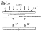
- phase shift mask 15 is, as shown in FIG. 4, a transparent photo mask 16 provided with a shifter 17 thereon.
- the phase shift mask 15 is irradiated with an ultraviolet ray, the intensity distribution of a light transmitted by the phase shift mask 15 is enlarged locally at the edges of the shifter 17. Therefore, by exposing a positive type resist with the phase shift mask 15, the minute dummy gate 12 can be produced on the semiconductor substrate 1, and finally, the gate electrode 8 with a minute gate length can be obtained.
- a gate length of about 0.5 ⁇ m is the limit, and it is very difficult to realize a minute gate length shorter than about 0.5 ⁇ m.
- the method of using the mixing layer 10 as in the above-mentioned second prior art method since the mixing layer 10 is formed by the die pattern for forming the mixing layer (the opening 5 of the lower resist 4), a 0.4 ⁇ m gate length is the limit with respect to the 0.5 ⁇ m limit of the ordinary light exposure method. Furthermore, this method also has a problem in that the phase shift mask method, which is effective in achieving a minute gate pattern, cannot be used. Although a phase shift mask 15 can be used for forming an opening 5 in a lower resist 4, with a negative type resist used for the lower resist 4, the negative type resist has, in general, a poor resolution, and thus a minute pattern cannot be obtained. Besides, a high resolution negative type resist represented by the chemically amplified type has a poor reproductivity, and is difficult in control.
- a minute gate length can be realized by the method of forming the gate electrode 8, using the dummy gate 12 as in the above-mentioned third prior art method, realization of a further minute gate length is desired.
- the insulating film 13 exists in the vicinity of the T-section gate electrode in the method using the dummy gate 12, a problem is involved in that the gate parasitic capacity is increased so that the high frequency characteristics of the field effect transistor are deteriorated.
- large size equipment is needed for forming the insulating film 13 to be used for reversing the dummy gate 12, the production cost is increased, and moreover, damage is easily introduced into the semiconductor substrate 1.
- the present invention can solve the above-mentioned problems associated with the conventional art and provide a method for forming a resist pattern, capable of obtaining a further minute electrode pattern.
- the present invention also provide a method for forming a gate electrode having a fine gate length.
- the method for forming a resist pattern comprises the steps of: forming a dummy pattern on a semiconductor substrate using one type of a photosensitive resist; applying a resist mask on the semiconductor substrate so as to bury the dummy pattern using an opposite type of a photosensitive resist; forming a mixing layer at the interface between the dummy pattern and the resist mask by applying a heat treatment; and dissolving and removing the dummy pattern with an etchant in which the mixing layer and the resist mask are indissoluble so as to form an opening having a space width smaller than a width of the dummy pattern in the resist mask.
- the method for forming gate electrode on a semiconductor substrate comprises the steps of depositing a gate electrode material in the opening of the resist mask and over the resist mask and removing the resist mask to form a gate electrode on the semiconductor substrate, after forming the resist mask in accordance with the aforementioned method.
- a field effect transistor having a minute gate electrode with excellent high frequency characteristics can be manufactured inexpensively with a good yield.
- a method for forming a fine resist pattern according to the present invention comprises the steps of: forming a dummy pattern on a semiconductor substrate with one type of a photosensitive resist; applying a resist mask on the semiconductor substrate so as to bury the dummy pattern with the other type of a photosensitive resist; forming a mixing layer at the interface between the dummy pattern and the resist mask by applying a heat treatment; and dissolving and removing the dummy pattern with am etchant, by which the mixing layer and the resist mask are indissoluble.
- Photosensitive resist refers to positive and negative ones
- a minute pattern can be obtained by using a dummy pattern such as a dummy gate.
- a phase shift mask an extremely minute pattern can be obtained. Since a mixing layer is formed on the surface of a dummy pattern, utilizing a generation of a mixing layer indissoluble by a developer at the interface between the different photosensitive resists in the present invention, the width of the opening formed after dissolving and removing the dummy pattern is narrower than the width of the original dummy pattern owing to the remaining mixing layer. Therefore, according to the present invention, a further minute opening pattern can be obtained compared with a pattern obtained by the dummy gate method, or the like. Or by forming a metal pattern, or the like, such as a gate electrode in the opening pattern, a further minute pattern compared with a metal pattern of the conventional dummy gate method can be obtained.
- a dummy pattern is formed with a positive type resist, and a resist mask is formed with a negative type resist. Since a minute dummy pattern can be obtained with light exposure by the use of a positive type resist, a pattern to be obtained finally can further be minute. In this case, by using an alkaline developer after exposing the dummy pattern by dry etching the resist mask, the dummy pattern can be dissolved and removed selectively.
- the present invention since electron exposure is not needed, a minute gate electrode can be produced easily. And further, since the insulating film does not need to be formed, production equipment can be simplified, and the production cost can be lowered. Furthermore, since the vicinity of the gate electrode can be a space by removing the resist mask and the mixing layer after forming the gate electrode in the opening of the mixing layer, increase of the gate parasitic capacity can be restrained and deterioration of the high frequency characteristics of the field effect transistor can be prevented.
- FIGS. 5A to 5F are diagrams for explaining a method for forming a gate electrode according to one embodiment of the present invention. It shows the case of forming a T-section gate electrode in a field effect transistor, such as GaAs MESFET, HFET (hetero junction field effect transistor), or the like.
- a field effect transistor such as GaAs MESFET, HFET (hetero junction field effect transistor), or the like.
- a source electrode 22 and a drain electrode 23 are provided on a compound semiconductor substrate 21 such as a GaAs substrate, or the like, with an epitaxial growth layer(s) formed thereon.
- a dummy gate 24 with, for example, a 0.3 ⁇ m width (gate length of the dummy gate) is formed by forming a positive type resist (such as Pfi26A: produced by Sumitomo Chemical Industry Corp., Japan) with a 1 ⁇ m film thickness on the semiconductor substrate 21 provided with the source and drain electrodes 22, 23, and light exposure with a phase shift mask and development (FIG. 5A).
- a negative type resist 25 (for example, OMR-85: produced by Tokyo Oka Kogyo Corp., Japan) is applied and formed with a 1 ⁇ m film thickness so as to cover the dummy gate 24 (FIG. 5B).
- a heat treatment is conducted with a 20°C to 120°C temperature range, 60 minutes or less treatment condition.
- a mixing layer 26 indissoluble by an alkaline developer is formed as shown in FIG. 6 at the interface between the dummy gate 24 comprising the positive type resist and the negative type resist 25 by diffusion or reaction of the positive type resist and the negative type resist.
- the mixing layer 26 can be formed with a stable film thickness.
- the negative type resist 25 is removed by the dry etching method using, for example, an O 2 gas.
- the entirety of the semiconductor substrate 21 is light exposed for sufficiently exposing the positive type resist, which is the dummy gate 24, and then the dummy gate 24 is removed with an ordinary alkaline developer (for example, NMD-3: produced by Tokyo Oka Kogyo Corp., Japan).
- an ordinary alkaline developer for example, NMD-3: produced by Tokyo Oka Kogyo Corp., Japan.
- an insulating film needs not be formed for reversing the dummy gate 24, and thus the semiconductor substrate 21 is not damaged.
- the mixing layer 26 is indissoluble and not exposed or removed in the alkaline development, the targeted opening size can be obtained with certainty.
- the opening width of the reversed opening 27 is further narrower than the width of the minute dummy gate 24 formed with the phase shift mask, and thus a further minute opening pattern compared with the opening width obtained by merely reversing the dummy gate 24 can be obtained.
- an upper resist 28 is applied with an image reversing resist (for example, AZ5214E: Produced by Hoechst Japan Corp., Japan), and an inverted tapered opening pattern 29 larger than the opening 27 is formed in the upper resist 28 (FIG. 5E).
- an image reversing resist for example, AZ5214E: Produced by Hoechst Japan Corp., Japan
- a T-section gate electrode 30 is formed by the lift-off method (FIG. 5F).
- the gate electrode 30 By forming the gate electrode 30 as mentioned above, since the dummy gate 24 with a minute line width can be obtained by the phase shift mask method, suited or forming a minute pattern with light exposure, and further, the mixing layer 26 indissoluble with a developer is formed at the interface between the dummy gate 24 and the negative type resist 25, which is the reversing material thereof, a gate opening pattern having a size narrower than the resolution limit or the initial dummy gate length can be obtained by removing the dummy gate 24 by development, and thus a gate electrode with a further minute gate length can be obtained compared with the conventional dummy gate method.
- FIG. 8 shows the line width of a dummy gate formed with a phase shift mask (dummy gate length) and a reversed pattern width obtained by the method of the present invention (opening width of the mixing layer).
- the gate width can be shortened by about 0.05 to 0.1 ⁇ m.
- the resist used for forming the gate electrode is completely removed finally, a gap is formed in the vicinity of the T gate electrode, and thus the parasitic capacity can be smaller. Furthermore, unlike the conventional dummy gate method explained as the third prior art method, a minute pattern can be formed without the need of strict process administration in the minute processing of the dummy gate. Moreover, since an insulating film is not used, production cost increase by the insulating film formation, increase of the parasitic capacity, and introduction of damage can be avoided. Further, since the negative type resist used in this embodiment has both functions as the reversing material and the mixing formation material, the advantages of the second and third prior arts can be obtained inexpensively.
Landscapes
- Engineering & Computer Science (AREA)
- Physics & Mathematics (AREA)
- Condensed Matter Physics & Semiconductors (AREA)
- General Physics & Mathematics (AREA)
- Manufacturing & Machinery (AREA)
- Computer Hardware Design (AREA)
- Microelectronics & Electronic Packaging (AREA)
- Power Engineering (AREA)
- Junction Field-Effect Transistors (AREA)
- Electrodes Of Semiconductors (AREA)
- Exposure Of Semiconductors, Excluding Electron Or Ion Beam Exposure (AREA)
- Photosensitive Polymer And Photoresist Processing (AREA)
Applications Claiming Priority (2)
| Application Number | Priority Date | Filing Date | Title |
|---|---|---|---|
| JP22506298A JP3591762B2 (ja) | 1998-08-07 | 1998-08-07 | パターンの形成方法 |
| JP22506298 | 1998-08-07 |
Publications (3)
| Publication Number | Publication Date |
|---|---|
| EP0978869A2 true EP0978869A2 (de) | 2000-02-09 |
| EP0978869A3 EP0978869A3 (de) | 2002-01-16 |
| EP0978869B1 EP0978869B1 (de) | 2009-03-25 |
Family
ID=16823449
Family Applications (1)
| Application Number | Title | Priority Date | Filing Date |
|---|---|---|---|
| EP99114433A Expired - Lifetime EP0978869B1 (de) | 1998-08-07 | 1999-07-22 | Verfahren zur Herstellung eines kleinen Resistmusters sowie Verfahren zur Herstellung einer Gateelektrode |
Country Status (5)
| Country | Link |
|---|---|
| US (1) | US6180528B1 (de) |
| EP (1) | EP0978869B1 (de) |
| JP (1) | JP3591762B2 (de) |
| KR (1) | KR100303767B1 (de) |
| DE (1) | DE69940628D1 (de) |
Cited By (1)
| Publication number | Priority date | Publication date | Assignee | Title |
|---|---|---|---|---|
| US6881688B2 (en) | 2002-02-05 | 2005-04-19 | Bernd E. Maile | Method of fabricating a vertically profiled electrode and semiconductor device comprising such an electrode |
Families Citing this family (4)
| Publication number | Priority date | Publication date | Assignee | Title |
|---|---|---|---|---|
| JP4093395B2 (ja) * | 2001-08-03 | 2008-06-04 | 富士通株式会社 | 半導体装置とその製造方法 |
| JP2003273131A (ja) * | 2002-01-10 | 2003-09-26 | Murata Mfg Co Ltd | 微細電極形成用マスキング部材およびその製造方法、電極の形成方法ならびに電界効果トランジスタ |
| US7115488B2 (en) * | 2003-08-29 | 2006-10-03 | Semiconductor Energy Laboratory Co., Ltd. | Method of manufacturing semiconductor device |
| JP5521447B2 (ja) | 2009-09-07 | 2014-06-11 | 富士通株式会社 | 半導体装置の製造方法 |
Citations (6)
| Publication number | Priority date | Publication date | Assignee | Title |
|---|---|---|---|---|
| JPS6290979A (ja) * | 1985-10-17 | 1987-04-25 | Matsushita Electric Ind Co Ltd | 半導体装置の製造方法 |
| JPH02115855A (ja) * | 1988-10-26 | 1990-04-27 | Matsushita Electron Corp | 半導体装置の製造方法 |
| JPH02156244A (ja) * | 1988-12-08 | 1990-06-15 | Oki Electric Ind Co Ltd | パターン形成方法 |
| JPH03147338A (ja) * | 1989-11-02 | 1991-06-24 | New Japan Radio Co Ltd | 半導体装置の製造方法 |
| JPH04290421A (ja) * | 1991-03-19 | 1992-10-15 | Kobe Steel Ltd | リフトオフ法に適したフォトレジストパターンの形成方法 |
| JPH05166717A (ja) * | 1991-12-16 | 1993-07-02 | Mitsubishi Electric Corp | 微細パターン形成方法 |
Family Cites Families (2)
| Publication number | Priority date | Publication date | Assignee | Title |
|---|---|---|---|---|
| JP2723405B2 (ja) | 1991-11-12 | 1998-03-09 | 松下電器産業株式会社 | 微細電極の形成方法 |
| JP3249317B2 (ja) * | 1994-12-12 | 2002-01-21 | 富士通株式会社 | パターン作成方法 |
-
1998
- 1998-08-07 JP JP22506298A patent/JP3591762B2/ja not_active Expired - Lifetime
-
1999
- 1999-07-19 US US09/356,547 patent/US6180528B1/en not_active Expired - Lifetime
- 1999-07-22 EP EP99114433A patent/EP0978869B1/de not_active Expired - Lifetime
- 1999-07-22 DE DE69940628T patent/DE69940628D1/de not_active Expired - Lifetime
- 1999-08-07 KR KR1019990032412A patent/KR100303767B1/ko active IP Right Grant
Patent Citations (6)
| Publication number | Priority date | Publication date | Assignee | Title |
|---|---|---|---|---|
| JPS6290979A (ja) * | 1985-10-17 | 1987-04-25 | Matsushita Electric Ind Co Ltd | 半導体装置の製造方法 |
| JPH02115855A (ja) * | 1988-10-26 | 1990-04-27 | Matsushita Electron Corp | 半導体装置の製造方法 |
| JPH02156244A (ja) * | 1988-12-08 | 1990-06-15 | Oki Electric Ind Co Ltd | パターン形成方法 |
| JPH03147338A (ja) * | 1989-11-02 | 1991-06-24 | New Japan Radio Co Ltd | 半導体装置の製造方法 |
| JPH04290421A (ja) * | 1991-03-19 | 1992-10-15 | Kobe Steel Ltd | リフトオフ法に適したフォトレジストパターンの形成方法 |
| JPH05166717A (ja) * | 1991-12-16 | 1993-07-02 | Mitsubishi Electric Corp | 微細パターン形成方法 |
Non-Patent Citations (6)
| Title |
|---|
| PATENT ABSTRACTS OF JAPAN vol. 011, no. 292 (E-543), 19 September 1987 (1987-09-19) -& JP 62 090979 A (MATSUSHITA ELECTRIC IND CO LTD), 25 April 1987 (1987-04-25) * |
| PATENT ABSTRACTS OF JAPAN vol. 014, no. 337 (P-1079), 20 July 1990 (1990-07-20) -& JP 02 115855 A (MATSUSHITA ELECTRON CORP), 27 April 1990 (1990-04-27) * |
| PATENT ABSTRACTS OF JAPAN vol. 014, no. 405 (P-1100), 31 August 1990 (1990-08-31) -& JP 02 156244 A (OKI ELECTRIC IND CO LTD), 15 June 1990 (1990-06-15) * |
| PATENT ABSTRACTS OF JAPAN vol. 015, no. 371 (E-1113), 18 September 1991 (1991-09-18) -& JP 03 147338 A (NEW JAPAN RADIO CO LTD), 24 June 1991 (1991-06-24) * |
| PATENT ABSTRACTS OF JAPAN vol. 017, no. 101 (E-1327), 2 March 1993 (1993-03-02) -& JP 04 290421 A (KOBE STEEL LTD), 15 October 1992 (1992-10-15) * |
| PATENT ABSTRACTS OF JAPAN vol. 017, no. 568 (E-1447), 14 October 1993 (1993-10-14) -& JP 05 166717 A (MITSUBISHI ELECTRIC CORP), 2 July 1993 (1993-07-02) * |
Cited By (2)
| Publication number | Priority date | Publication date | Assignee | Title |
|---|---|---|---|---|
| US6881688B2 (en) | 2002-02-05 | 2005-04-19 | Bernd E. Maile | Method of fabricating a vertically profiled electrode and semiconductor device comprising such an electrode |
| EP1335418B1 (de) * | 2002-02-05 | 2005-09-07 | Bernd E. Dr. Maile | Verfahren zur Herstellung einer T-förmigen Elektrode |
Also Published As
| Publication number | Publication date |
|---|---|
| EP0978869A3 (de) | 2002-01-16 |
| DE69940628D1 (de) | 2009-05-07 |
| KR100303767B1 (ko) | 2001-11-01 |
| KR20000017166A (ko) | 2000-03-25 |
| EP0978869B1 (de) | 2009-03-25 |
| US6180528B1 (en) | 2001-01-30 |
| JP2000058418A (ja) | 2000-02-25 |
| JP3591762B2 (ja) | 2004-11-24 |
Similar Documents
| Publication | Publication Date | Title |
|---|---|---|
| US5264382A (en) | Method of producing semiconductor device using dummy gate structure | |
| EP0516408A2 (de) | Verfahren zur Herstellung einer T-Gatestruktur über einem Substrat mit einem mikroelektronischen Bauelement | |
| US4975382A (en) | Method of making a self-aligned field-effect transistor by the use of a dummy-gate | |
| EP0801418B1 (de) | Herstellungsverfahren einer T-förmigen Gate-Elektrode in einem Halbleiterbauelement, und die T-förmige Gate-Elektrode | |
| JP2000022131A (ja) | 半導体装置およびその製造方法 | |
| US6153499A (en) | Method of manufacturing semiconductor device | |
| JPH0787195B2 (ja) | ショットキゲート電界効果トランジスタの製造方法 | |
| EP0978869B1 (de) | Verfahren zur Herstellung eines kleinen Resistmusters sowie Verfahren zur Herstellung einer Gateelektrode | |
| US5693548A (en) | Method for making T-gate of field effect transistor | |
| US5702960A (en) | Method for manufacturing polysilicon thin film transistor | |
| US6727126B2 (en) | Masking member for forming fine electrode and manufacturing method therefor, method for forming electrode, and field effect transistor | |
| US4935377A (en) | Method of fabricating microwave FET having gate with submicron length | |
| US5925902A (en) | Semiconductor device having a schottky film with a vertical gap formed therein | |
| KR100228385B1 (ko) | 반도체 소자의 게이트 전극 제조 방법 | |
| JPH1140578A (ja) | 半導体装置及びその製造方法 | |
| JP2837036B2 (ja) | ゲート電極の形成方法 | |
| JP2569336B2 (ja) | 半導体装置の製造方法 | |
| JPS6341078A (ja) | 半導体装置の製造方法 | |
| KR100672783B1 (ko) | 반도체 소자의 제조 방법 | |
| JPH0653246A (ja) | 電界効果トランジスタの製法 | |
| JPH0684950A (ja) | 電界効果トランジスタの製造方法 | |
| JPH0684954A (ja) | 半導体装置の製造方法 | |
| JP2003031594A (ja) | 半導体装置の製造方法 | |
| JPH05218095A (ja) | 半導体装置の製造方法 | |
| KR19980017256A (ko) | 반도체 소자의 제조 방법 |
Legal Events
| Date | Code | Title | Description |
|---|---|---|---|
| PUAI | Public reference made under article 153(3) epc to a published international application that has entered the european phase |
Free format text: ORIGINAL CODE: 0009012 |
|
| 17P | Request for examination filed |
Effective date: 19990722 |
|
| AK | Designated contracting states |
Kind code of ref document: A2 Designated state(s): AT BE CH CY DE DK ES FI FR GB GR IE IT LI LU MC NL PT SE Kind code of ref document: A2 Designated state(s): DE FR GB |
|
| AX | Request for extension of the european patent |
Free format text: AL;LT;LV;MK;RO;SI |
|
| PUAL | Search report despatched |
Free format text: ORIGINAL CODE: 0009013 |
|
| AK | Designated contracting states |
Kind code of ref document: A3 Designated state(s): AT BE CH CY DE DK ES FI FR GB GR IE IT LI LU MC NL PT SE |
|
| AX | Request for extension of the european patent |
Free format text: AL;LT;LV;MK;RO;SI |
|
| RIC1 | Information provided on ipc code assigned before grant |
Free format text: 7H 01L 21/28 A, 7H 01L 21/027 B, 7G 03F 7/00 B, 7H 01L 21/285 B, 7H 01L 21/338 B |
|
| AKX | Designation fees paid |
Free format text: DE FR GB |
|
| 17Q | First examination report despatched |
Effective date: 20060906 |
|
| RAP1 | Party data changed (applicant data changed or rights of an application transferred) |
Owner name: MURATA MANUFACTURING CO., LTD. |
|
| GRAP | Despatch of communication of intention to grant a patent |
Free format text: ORIGINAL CODE: EPIDOSNIGR1 |
|
| GRAS | Grant fee paid |
Free format text: ORIGINAL CODE: EPIDOSNIGR3 |
|
| GRAA | (expected) grant |
Free format text: ORIGINAL CODE: 0009210 |
|
| AK | Designated contracting states |
Kind code of ref document: B1 Designated state(s): DE FR GB |
|
| REG | Reference to a national code |
Ref country code: GB Ref legal event code: FG4D |
|
| REF | Corresponds to: |
Ref document number: 69940628 Country of ref document: DE Date of ref document: 20090507 Kind code of ref document: P |
|
| PLBE | No opposition filed within time limit |
Free format text: ORIGINAL CODE: 0009261 |
|
| STAA | Information on the status of an ep patent application or granted ep patent |
Free format text: STATUS: NO OPPOSITION FILED WITHIN TIME LIMIT |
|
| 26N | No opposition filed |
Effective date: 20091229 |
|
| GBPC | Gb: european patent ceased through non-payment of renewal fee |
Effective date: 20090722 |
|
| REG | Reference to a national code |
Ref country code: FR Ref legal event code: ST Effective date: 20100331 |
|
| PG25 | Lapsed in a contracting state [announced via postgrant information from national office to epo] |
Ref country code: FR Free format text: LAPSE BECAUSE OF NON-PAYMENT OF DUE FEES Effective date: 20090731 |
|
| PG25 | Lapsed in a contracting state [announced via postgrant information from national office to epo] |
Ref country code: GB Free format text: LAPSE BECAUSE OF NON-PAYMENT OF DUE FEES Effective date: 20090722 |
|
| PGFP | Annual fee paid to national office [announced via postgrant information from national office to epo] |
Ref country code: DE Payment date: 20180723 Year of fee payment: 20 |
|
| REG | Reference to a national code |
Ref country code: DE Ref legal event code: R071 Ref document number: 69940628 Country of ref document: DE |